General Description
The MAX2420/MAX2421/MAX2422/MAX2460/MAX2463
are highly integrated front-end ICs that provide the lowest
cost solution for cordless phones and ISM-band radios
operating in the 900MHz band. All devices incorporate
transmit and receive image-reject mixers to reduce filter
cost. They operate with a +2.7V to +4.8V power supply,
allowing direct connection to a three-cell battery stack.
The receive path incorporates an adjustable-gain LNA
and an image-reject downconverter with 35dB image
suppression. These features yield excellent combined
downconverter noise figure (4dB) and high linearity with
an input third-order intercept point (IP3) of up to +2dBm.
The transmitter consists of a variable-gain IF amplifier
with more than 35dB control range, an image-reject
upconverter with 35dB image rejection, and a power-
amplifier (PA) predriver that produces up to +2dBm (in
some applications serving as the final power stage).
All devices include an on-chip local oscillator (LO),
requiring only an external varactor-tuned LC tank for
operation. The integrated divide-by-64/65 dual-modulus
prescaler can also be set to a direct mode, in which it
acts as an LO buffer amplifier. Four separate power-
down inputs can be used for system power manage-
ment, including a 0.5µA shutdown mode. These parts
are compatible with commonly used modulation
schemes such as FSK, BPSK, and QPSK, as well as fre-
quency hopping and direct sequence spread-spectrum
systems. All devices come in a 28-pin SSOP package.
For applications using direct VCO or BPSK transmit mod-
ulation, as well as receive image rejection, consult the
MAX2424/MAX2426 data sheet. For receive-only devices,
refer to the MAX2440/MAX2441/MAX2442 data sheet.
________________________Applications
Cordless Phones
Spread-Spectrum Communications
Wireless Telemetry
Two-Way Paging
Wireless Networks
Features
o Receive/Transmit Mixers with 35dB Image Rejection
o Adjustable-Gain LNA
o Up to +2dBm Combined Receiver Input IP3
o 4dB Combined Receiver Noise Figure
o >35dB of Transmit Power Control Range
o PA Predriver Provides up to +2dBm
o Low Current Consumption: 23mA Receive
26mA Transmit
9.5mA Oscillator
o 0.5µA Shutdown Mode
o Operates from Single +2.7V to +4.8V Supply
MAX2420/MAX2421/MAX2422/MAX2460/MAX2463
900MHz Image-Reject Transceivers
________________________________________________________________ Maxim Integrated Products
1
28
27
26
25
24
23
22
21
20
19
18
17
16
15
1
2
3
4
5
6
7
8
9
10
11
12
13
14
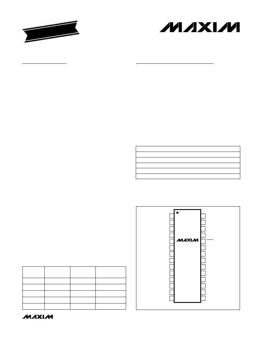
GND
GND
GND
TANK
TXON
PREOUT
PREGND
MOD
DIV1
VCOON
RXON
CAP2
N.C.
TXIN
LNAGAIN
TXOUT
GND
GND
RXIN
TXGAIN
RXOUT
CAP1
SSOP
TOP VIEW
MAX2420
MAX2421
MAX2422
MAX2460
MAX2463
TANK
V
CC
V
CC
V
CC
V
CC
V
CC
___________________Pin Configuration
19-1234; Rev 5; 8/03
PART
MAX2420EAI
MAX2421EAI
MAX2422EAI
-40°C to +85°C
-40°C to +85°C
-40°C to +85°C
TEMP RANGE
PIN-PACKAGE
28 SSOP
28 SSOP
28 SSOP
_______________Ordering Information
MAX2460EAI
-40°C to +85°C
28 SSOP
Functional Diagram appears on last page.
MAX2463EAI
-40°C to +85°C
28 SSOP
High side
INJECTION
TYPE
f
RF
+ 10.7
LO FREQ
(MHz)
High side
High side
f
RF
+ 70
f
RF
+ 46
MAX2422
MAX2421
70
46
Low side
f
RF
- 110
MAX2463
110
MAX2420
PART
10.7
IF FREQ
(MHz)
______________________Selector Guide
Low side
f
RF
- 10.7
MAX2460
10.7
For pricing, delivery, and ordering information, please contact Maxim/Dallas Direct! at
1-888-629-4642, or visit Maxim's website at www.maxim-ic.com.
EVALUATION KIT
AVAILABLE

µA
MAX2420/MAX2421/MAX2422/MAX2460/MAX2463
900MHz Image-Reject Transceivers
2
_______________________________________________________________________________________
ABSOLUTE MAXIMUM RATINGS
DC ELECTRICAL CHARACTERISTICS
(V
CC
= +2.7V to +4.8V, no RF signals applied, LNAGAIN = TXGAIN = open, VCOON = 2.4V, RXON = TXON = MOD = DIV1 = 0.45V,
PREGND = GND, T
A
= T
MIN
to T
MAX
. Typical values are at T
A
= +25°C, V
CC
= +3.3V, unless otherwise noted.) (Note 1)
Stresses beyond those listed under "Absolute Maximum Ratings" may cause permanent damage to the device. These are stress ratings only, and functional
operation of the device at these or any other conditions beyond those indicated in the operational sections of the specifications is not implied. Exposure to
absolute maximum rating conditions for extended periods may affect device reliability.
Note 1:
25°C guaranteed by production test, <25°C guaranteed through correlation to worst-case temperature testing.
Note 2: Calculated by measuring the combined oscillator and prescaler supply current and subtracting the oscillator supply current.
Note 3: Calculated by measuring the combined oscillator and LO buffer supply current and subtracting the oscillator supply current.
Note 4: Calculated by measuring the combined receive and oscillator supply current and subtracting the oscillator supply current.
With LNAGAIN = GND, the supply current drops by 4.5mA.
Note 5: Calculated by measuring the combined transmit and oscillator supply current and subtracting the oscillator supply current.
V
CC
to GND ...........................................................-0.3V to +5.5V
TXIN Input Power (330
system) ......................................-8dBm
Voltage on TXOUT......................................-0.3V to (V
CC
+ 1.0V)
Voltage on TXGAIN, LNAGAIN, TXON,
RXON, VCOON, DIV1, MOD ....................-0.3V to (V
CC
+ 0.3V)
RXIN Input Power..............................................................10dBm
TANK, TANK Input Power ...................................................2dBm
Continuous Power Dissipation (T
A
= +70°C)
SSOP (derate 9.50mW/°C above +70°C) ......................762mW
Operating Temperature Range
MAX242_EAI/MAX246_EAI ................................-40°C to +85°C
Junction Temperature ......................................................+150°C
Storage Temperature Range .............................-65°C to +165°C
Lead Temperature (soldering, 10s) .................................+300°C
PARAMETER
MIN
TYP
MAX
UNITS
Receive Supply Current (Note 4)
23
36
mA
Prescaler Supply Current
(buffer mode) (Note 3)
5.4
8.5
mA
Oscillator Supply Current
Supply-Voltage Range
2.7
4.8
V
9.5
14
mA
Prescaler Supply Current
(divide-by-64/65 mode) (Note 2)
4.2
6
mA
CONDITIONS
RXON = 2.4V, PREGND = floating
DIV1 = 2.4V
PREGND = floating
Digital Input Voltage Low
0.45
V
Transmitter Supply Current (Note 5)
26
42
mA
0.5
RXON, TXON, DIV1, VCOON, MOD
RXON = 0.45V, TXON = 2.4V, PREGND = floating
VCOON = RXON = TXON =
MOD = DIV1 = GND
Digital Input Current
±1
±10
µA
Voltage on any one digital input = V
CC
or GND
Digital Input Voltage High
V
2.4
RXON, TXON, DIV1, VCOON, MOD
Shutdown Supply Current
10
µA
T
A
= +25°C
T
A
= T
MIN
to T
MAX
CAUTION! ESD SENSITIVE DEVICE

LNAGAIN = 1V
AC ELECTRICAL CHARACTERISTICS
(MAX242X/246X EV kit, V
CC
= +3.3V; f
LO
= 925.7MHz (MAX2420), f
LO
= 961MHz (MAX2421), f
LO
= 985MHz (MAX2422),
f
LO
= 904.3MHz (MAX2460); f
LO
= 805MHz (MAX2463); f
RXIN
= 915MHz; P
RXIN
= -35dBm; P
TXIN
= -15dBm (330
); LNAGAIN = 2V;
TXGAIN = V
CC
; VCOON = 2.4V; RXON = TXON = MOD = DIV1 = PREGND = GND; T
A
= +25°C; unless otherwise noted.)
MAX2420/MAX2421/MAX2422/MAX2460/MAX2463
900MHz Image-Reject Transceivers
_______________________________________________________________________________________
3
CONDITIONS
UNITS
MIN
TYP
MAX
PARAMETER
MHz
800
1000
Input Frequency Range
(Notes 6, 7)
MAX2421
36
46
55
MAX2420/MAX2460
8.5
10.7
12.5
MAX2463
MHz
86
110
132
IF Frequency Range
(Notes 6, 7)
20
22
24.5
MAX2422
dB
26
35
Image Frequency Rejection
55
70
85
LNAGAIN = V
CC
,
T
A
= +25°C
18
20
22.5
18
24
19.5
25
LNAGAIN = 1V
12
DIV1 = V
CC
4
5
LNAGAIN = V
CC
,
T
A
= T
MIN
to T
MAX
(Note 6)
LNAGAIN = GND
dB
-16
Conversion Power Gain (Note 8)
17
23
19
21
23.5
dB
12
Noise Figure (Notes 6, 8)
LNAGAIN = 1V
dBm
-8
Input Third-Order Intercept
(Notes 6, 9)
LNAGAIN = V
CC
-19
-17
(Note 10)
ns
500
Receiver Turn-On Time
MHz
800
1000
Output Frequency Range
(Notes 6, 7)
Receiver on or off
dBm
-60
LO to RXIN Leakage
MAX2421
36
46
55
MAX2463
MHz
86
110
132
IF Frequency Range
MAX2420/MAX2460
MAX2422
55
70
85
dB
11
13.5
16
9
12
14.5
10
12.5
15
dB
26
35
Image Frequency Rejection
8.5
10.7
12.5
T
A
= +25°C
8
11
13.5
10
15.5
T
A
= T
MIN
to T
MAX
(Note 6)
8
14
Conversion Gain
9
15
10.5
16.5
LNAGAIN = 1V
dBm
-18
Input 1dB Compression
LNAGAIN = V
CC
-26
MAX2420/MAX2421/MAX2460
MAX2422
MAX2463
MAX2420/MAX2421/MAX2460
MAX2422
MAX2463
MAX2420/2460
MAX2421
MAX2422
MAX2463
MAX2420/2460
MAX2421
MAX2422
MAX2463
LNAGAIN = V
CC
LNAGAIN = 1V
RECEIVER (RXON = 2.4V)
TRANSMITTER (TXON = 2.4V)

MAX2420/MAX2421/MAX2422/MAX2460/MAX2463
900MHz Image-Reject Transceivers
4
_______________________________________________________________________________________
AC ELECTRICAL CHARACTERISTICS (continued)
(MAX242X/246X EV kit, V
CC
= +3.3V; f
LO
= 925.7MHz (MAX2420), f
LO
= 961MHz (MAX2421), f
LO
= 985MHz (MAX2422),
f
LO
= 904.3MHz (MAX2460); f
LO
= 805MHz (MAX2463); f
RXIN
= 915MHz; P
RXIN
= -35dBm; P
TXIN
= -15dBm (330
); LNAGAIN = 2V;
TXGAIN = V
CC
; VCOON = 2.4V; RXON = TXON = MOD = DIV1 = PREGND = GND; T
A
= +25°C; unless otherwise noted.)
PARAMETER
MIN
TYP
MAX
UNITS
Transmitter Turn-On Time (Note 14)
Gain Control Range (Note 13)
36
TXGAIN Control Slope (Note 13)
dB
33
dB/V
400
ns
Oscillator Phase Noise
Output 1dB Compression
Oscillator Frequency Range
(Notes 6, 15)
2
dBm
690
1100
MHz
82
dBc/Hz
8
10kHz offset (Note 16)
Standby to TX, or standby to RX
CONDITIONS
1V
TXGAIN 2V
Note 6:
Guaranteed by design and characterization.
Note 7:
Image rejection typically falls to 30dBc at the frequency extremes.
Note 8:
Refer to the Typical Operating Characteristics for plots showing receiver gain vs. LNAGAIN voltage, input IP3 vs.
LNAGAIN voltage, and noise figure vs. LNAGAIN voltage.
Note 9:
Two tones at P
RXIN
= -45dBm each, f1 = 915.0MHz and f2 = 915.2MHz.
Note 10: Time delay from RXON = 0.45V to RXON = 2.4V transition to the time the output envelope reaches 90% of its final value.
Note 11: Two tones at P
TXIN
= -21dBm each (330
), f1 = 10.6MHz, f2 = 10.8MHz (MAX2420/MAX2460), f1 = 45.9MHz,
f2 = 46.1MHz (MAX2421), f1 = 69.9MHz, f2 = 70.1MHz (MAX2422).
Note 12: Refer to the Typical Operating Characteristics for statistical data.
Note 13: Refer to the Typical Operating Characteristics for a plot showing transmitter gain vs. TXGAIN voltage.
Note 14: Time delay from TXON = 0.45V to TXON = 2.4V transition to the time the output envelope reaches 90% of its final value.
Note 15: Refers to useable operating range. Tuning range of any given tank circuit design is typically much narrower (refer to Figure 2).
Note 16: Using tank components L3 = 5.0nH (Coilcraft A02T), C2 = C3 = C26 = 3.3pF, R6 = R7 = 10
.
Note 17: This approximates a typical application in which TXOUT is followed by an external PA and a T/R switch with finite isolation.
Note 18: Relative to the rising edge of PREOUT.
Prescaler Output Level
500
mV
P-P
-11
-8
Required Modulus Setup Time
(Note 6)
10
ns
Z
L
= 100k
| |
10pF
DIV1 = 2.4V, Z
L
= 50
, T
A
= +25°C
Divide-by-64/65 mode (Note 18)
Required Modulus Hold Time
(Note 6)
0
ns
Divide-by-64/65 mode (Note 18)
RX to TX with P
RXIN
= -45dBm (RX mode) to
P
RXIN
= 0dBm (TX mode) (Note 17)
70
Oscillator Buffer Output Level
(Note 6)
-12
dBm
DIV1 = 2.4V, Z
L
= 50
, T
A
= T
MIN
to T
MAX
Oscillator Pulling
kHz
Output Third-Order Intercept
(Note 11)
11
dBm
Noise Figure
23
LO to TXOUT Suppression
(Note 12)
34
dBc
dB
OSCILLATOR AND PRESCALER

MAX2420/MAX2421/MAX2422/MAX2460/MAX2463
900MHz Image-Reject Transceivers
_______________________________________________________________________________________
5
24
28
26
34
32
30
40
38
36
42
-40
0
20
-20
40
60
80
100
RECEIVER SUPPLY CURRENT
vs. TEMPERATURE
MAX2420-01
TEMPERATURE (°C)
I
CC
(mA)
V
CC
= 2.7V
RXON = V
CC
PREGND = FLOATING
INCLUDES OSCILLATOR
CURRENT
V
CC
= 3.3V
V
CC
= 4.8V
26
30
28
36
34
32
44
42
40
38
46
-40
0
20
-20
40
60
80
100
TRANSMITTER SUPPLY CURRENT
vs. TEMPERATURE
MAX2420-02
TEMPERATURE (°C)
I
CC
(mA)
V
CC
= 2.7V
V
CC
= 3.3V
V
CC
= 4.8V
TXON = V
CC
PREGND = FLOATING
INCLUDES OSCILLATOR
CURRENT
0
1.0
0.5
2.5
2.0
1.5
4.0
3.5
3.0
4.5
-40
0
20
-20
40
60
80
100
SHUTDOWN SUPPLY CURRENT
vs. TEMPERATURE
MAX2420-03
TEMPERATURE (°C)
I
CC
(
µ
A)
V
CC
= 2.7V
V
CC
= 3.3V
V
CC
= 4.8V
VCOON = GND
25
20
15
10
5
0
-5
-10
-15
-20
0
0.5
1.0
1.5
2.0
RECEIVER GAIN vs. LNAGAIN
MAX2420-04
LNAGAIN VOLTAGE (V)
RECEIVER GAIN (dB)
ADJUSTABLE
GAIN
MAX
GAIN
LNA
PARTIALLY
BIASED
LNA
OFF
AVOID
THIS
REGION
RXON = V
CC
18
22
20
26
24
-40
0
20
-20
40
60
80
100
MAX2420
RECEIVER GAIN vs. TEMPERATURE
MAX2420-07
TEMPERATURE (°C)
RECEIVER GAIN (dB)
V
CC
= 2.7V
V
CC
= 3.3V
V
CC
= 4.8V
LNAGAIN = V
CC
RXON = V
CC
-20
-15
-10
-5
0
5
0
0.5
1.0
1.5
2.0
RECEIVER INPUT IP3 vs. V
LNAGAIN
MAX2420-05
LNAGAIN VOLTAGE (V)
IIP3 (dBm)
ADJUSTABLE
GAIN
AVOID
THIS
REGION
MAX
GAIN
LNA
PARTIALLY
BIASED
LNA
OFF
RXON = V
CC
0
5
15
10
25
20
30
40
35
0
0.5
1.0
1.5
2.0
RECEIVER NOISE FIGURE
vs. LNAGAIN
MAX2420-06
LNAGAIN VOLTAGE (V)
NOISE FIGURE (dB)
ADJUSTABLE
GAIN
AVOID
THIS
REGION
MAX
GAIN
LNA
PARTIALLY
BIASED
LNA
OFF
DIV1 = V
CC
RXON = V
CC
3.0
4.0
3.5
5.0
5.5
4.5
-40
0
20
-20
40
60
80
100
RECEIVER NOISE FIGURE vs.
TEMPERATURE AND SUPPLY VOLTAGE
MAX2420-08
TEMPERATURE (°C)
NOISE FIGURE (dB)
V
CC
= 2.7V
V
CC
= 3.3V
V
CC
= 4.8V
LNAGAIN = V
CC
RXON = V
CC
DIV1 = V
CC
-20
-16
-18
-8
-10
-6
-12
-14
-40
0
20
-20
40
60
80
100
RECEIVER INPUT IP3
vs. TEMPERATURE
MAX2420-09
TEMPERATURE (°C)
IIP3 (dBm)
LNAGAIN = 1V
LNAGAIN = 2V
RXON = V
CC
Typical Operating Characteristics
(MAX242X/246X EV kit, V
CC
= +3.3V; f
LO
= 925.7MHz (MAX2420), f
LO
= 961MHz (MAX2421), f
LO
= 985MHz (MAX2422), f
LO
= 904.3MHz
(MAX2460); f
LO
= 805MHz (MAX2463); f
RXIN
= 915MHz; P
RXIN
= -35dBm; P
TXIN
= -15dBm (330
); LNAGAIN = 2V; TXGAIN = V
CC
;
VCOON = 2.4V; RXON = TXON = MOD = DIV1 = PREGND = GND; T
A
= +25°C; unless otherwise noted.)