Äîêóìåíòàöèÿ è îïèñàíèÿ www.docs.chipfind.ru
General Description
The MAX1578/MAX1579 provide four regulated outputs
to meet all the voltage requirements for small active-
matrix TFT-LCD displays in handheld devices where
minimum external components and high efficiency are
required. Each device consists of three advanced
charge pumps for LCD bias power and a step-up con-
verter for driving up to 8 series white LEDs for back-
lighting. The input voltage range is from 2.7V to 5.5V.
The charge pumps provide fixed +5V, +15V, and -10V
for the LCD bias circuits. No external diodes are need-
ed. A high-efficiency, fractional (1.5x/2x) charge pump
followed by a low-dropout linear regulator provides +5V
to power the source driver. Automatic mode changing
achieves the highest conversion efficiency. Two multi-
stage, high-voltage charge pumps generate +15V and
-10V to provide V
ON
and V
OFF
, respectively. Utilizing a
unique clocking scheme and internal drivers, these
charge pumps eliminate parasitic charge-current glitch-
es and reduce maximum input current, resulting in low
electromagnetic emissions. The outputs are sequenced
during startup and shutdown. In shutdown, the outputs
are discharged to zero.
The high-efficiency inductor step-up converter drives
up to 8 white LEDs in series with a constant current to
provide backlighting. The series connection allows the
LED currents to be identical for uniform brightness and
minimizes the number of traces to the LEDs. The
MAX1578 regulates constant LED current over the
entire temperature range. The MAX1579 features a tem-
perature derating function to avoid overdriving the
white LEDs during high ambient temperatures, enabling
higher drive current below +42
°C.
The MAX1578/MAX1579 are available in space-saving
24-lead 4mm x 4mm thin QFN packages.
Applications
PDAs, Palmtops
Smart Phones
Internet Appliances
LCD Displays with White LED Backlight
Features
Four Regulators in One Package
Bias Power Using Charge Pumps
+5V at 25mA for Source Driver
+15V at 100µA for V
ON
-10V at 100µA for V
OFF
No External Diodes Required
Output Sequencing
POS, NEG, and MAIN Are Autodischarged
During Shutdown
LED Backlight Power Using Boost Converter
Series LED Connection for Uniform Illumination
Supports Up to 8 LEDs at 25mA (max)
900mW (max) Power
PWM or Analog Dimming Control
Overvoltage Protection
Low Input/Output Ripple
Soft-Start with Zero Inrush Current
Fast 1MHz PWM Operation for Small
Component Size
Temperature Derating Function (MAX1579)
High Efficiency
Bias: 83% (5.0V at 25mA, 15V/-10V at 100µA)
LED: 84% (6 LEDs at 20mA)
Uses Only Ceramic Capacitors and Only One
Inductor
Independent Enable Inputs for LED and Bias
Power
Thermal-Shutdown Protection
1µA Shutdown Current
Tiny 4mm x 4mm Thin QFN Package
MAX1578/MAX1579
Complete Bias and White LED Power Supplies
for Small TFT Displays
________________________________________________________________ Maxim Integrated Products
1
19-3359; Rev 0; 8/04
For pricing delivery, and ordering information please contact Maxim/Dallas Direct! at
1-888-629-4642, or visit Maxim's website at www.maxim-ic.com.
Ordering Information
EVALUATION KIT
AVAILABLE
PART
TEMP RANGE
PIN-PACKAGE
MAX1578
ETG
-40
°C to +85°C
24 Thin QFN 4mm x 4mm
(T2444-4)
MAX1579
ETG
-40
°C to +85°C
24 Thin QFN 4mm x 4mm
(T2444-4)
MAX1578/MAX1579
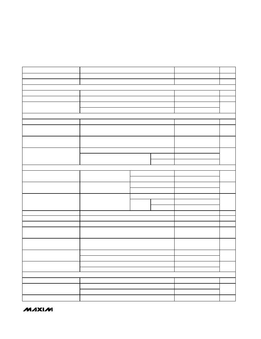
See Figure 3 for Typical Application Circuit.
ONBIAS
CD2
GND
NEG
PMPB
CD1
LX
CTRL
PGND
OUT
COMP
CS
CU1
CU3
MAIN
CU2
PMP
POS
19
20
21
22
23
24
1
2
3
4
5
6
18
17
16
15
14
13
12
11
10
9
8
7
MAX1578
MAX1579
THIN QFN
4mm x 4mm
C2N
C2P
C1N
IN
V
DD
C1P
Pin Configuration
MAX1578/MAX1579
Complete Bias and White LED Power Supplies
for Small TFT Displays
2
_______________________________________________________________________________________
ABSOLUTE MAXIMUM RATINGS
ELECTRICAL CHARACTERISTICS
(Circuit of Figure 3, V
IN
= 3V, CTRL = ONBIAS = IN, T
A
= -40
°C to +85°C, typical values are at T
A
= +25
°C, unless otherwise noted. Note 1)
Stresses beyond those listed under "Absolute Maximum Ratings" may cause permanent damage to the device. These are stress ratings only, and functional
operation of the device at these or any other conditions beyond those indicated in the operational sections of the specifications is not implied. Exposure to
absolute maximum rating conditions for extended periods may affect device reliability.
IN, CS, C1N, C2N, MAIN, ONBIAS, V
DD
to GND.....-0.3V to +6V
CTRL to GND..................-0.3V to the lesser of +6V or (V
IN
+ 2V)
LX, OUT to GND .....................................................-0.3V to +37V
COMP to GND .............................................-0.3V to (V
IN
+ 0.3V)
CU1 to MAIN ............................................................-0.3V to +6V
CU2 to CU1 ..............................................................-0.3V to +6V
CU3 to CU2 ..............................................................-0.3V to +6V
CU3 to POS ............................................................-0.3V to +18V
CU3 to GND ...........................................................-0.3V to +18V
POS to GND ...........................................................-0.3V to +18V
CD1 to MAIN ..........................................................+0.3V to -12V
CD1 to GND .............................................................+0.3V to -6V
CD2 to CD1 ..............................................................+0.3V to -6V
NEG to CD2..............................................................+0.3V to -6V
NEG, CD2 to GND..................................................+0.3V to -12V
C1P, C2P to GND ...........................................-0.3V to (V
IN
+ 6V)
PMP, PMPB to GND ................................-0.3V to (V
MAIN
+ 0.3V)
GND to PGND .......................................................-0.3V to +0.3V
I
LX
...................................................................................1.0A
RMS
Continuous Power Dissipation (T
A
= +70
°C)
24-Pin 4mm x 4mm Thin QFN
(derate 20.8mW/
°C above +70°C) .............................1667mW
Short-Circuit Duration (MAIN, POS, NEG)..................Continuous
Operating Temperature Range ...........................-40
°C to +85°C
Junction Temperature ......................................................+150
°C
Storage Temperature Range .............................-65
°C to +150°C
Lead Temperature (soldering, 10s) ................................ +300
°C
PARAMETER
CONDITIONS
MIN
TYP
MAX
UNITS
IN Operating Supply Range
2.7
5.5
V
IN Undervoltage-Lockout (UVLO)
Threshold
Rising edge, 30mV hysteresis
2.1
2.35
2.6
V
IN Quiescent Current
Switching
3
5
mA
T
A
= +25°C
0.4
1
IN Shutdown Current
V
CTRL
= V
ONBIAS
= 0V
T
A
= +85°C
1
µA
Thermal Shutdown
Rising temperature, 20°C hysteresis (typ)
+160
°C
MAIN CHARGE PUMP WITH LINEAR REGULATOR
Main Pump Efficiency
I
LOAD
= 25mA, V
IN
= 3.9V
83
%
V
IN
3.8V in 1.5x mode
9
20
V
DD
Charge-Pump Open-Loop
Output Impedance
V
IN
3.0V in 2.0x mode
7.5
20
Operating Frequency
200
250
300
kHz
V
DD
Output Voltage
Charge-pump pause threshold
5.2
5.5
5.7
V
V
IN
Fal l i ng S w i tchover to 2.0x M od e
3.75
3.85
3.95
V
V
IN
Ri si ng S w i tchover to 1.5x M od e
3.8
3.9
4.0
V
Quiescent Current
(Charge Pumps Only)
V
CTRL
= 0V, ONBIAS = IN
0.87
1.30
mA
V
MAIN
Regulation Voltage
0.1mA < I
LOAD
< 25mA
4.9
5.0
5.1
V
Discharge Switch Resistance
at V
MAIN
V
ONBIAS
= 0V
1
3
k
POS, NEG CHARGE PUMPS
Operating Frequency
12.0
15.6
19.5
kHz
Duty Cycle
50
%
POS Pump Efficiency
I
LOAD
= 100µA
97
%
POS Output Voltage
I
LOAD
= 0 to 100µA
13.9
14.7
15.3
V
P OS D i schar g e S w i tch Resi stance
V
ONBIAS
= 0V
3
6
k
NEG Pump Efficiency
I
LOAD
= -100µA
97
%
MAX1578/MAX1579
Complete Bias and White LED Power Supplies
for Small TFT Displays
_______________________________________________________________________________________
3
PARAMETER
CONDITIONS
MIN
TYP
MAX
UNITS
NEG Output Voltage
I
LOAD
= 0 to -100µA
-10.2
-9.8
-9.3
V
N E G D i schar g e S w i tch Resi stance
V
ONBIAS
= 0V
1.5
3
k
LOGIC INPUT (ONBIAS)
Logic Input Low Voltage
0.72
V
Logic Input High Voltage
1.6
V
T
A
= +25°C
0.01
1
Input Current
T
A
= +85°C
1
µA
LED BACKLIGHTING
Efficiency
LOAD = 6 LEDs in series at 20mA
84
%
OUT Voltage Range
(Note 2)
(V
IN
-
V
D1
)
32
V
Overvoltage-Lockout (OVLO)
Threshold
V
OUT
rising, 2V hysteresis
32
34
36
V
V
OUT
= 32V, V
CTRL
> 0.24V
10
20
32
T
A
= +25°C
0.01
1
OUT Input Bias Current
V
OUT
= V
IN
, V
CTRL
= 0
T
A
= +85°C
0.1
µA
ERROR AMPLIFIER
T
A
= +25°C
0.295
0.300
0.305
CTRL to CS Regulation
V
CTRL
= 1.5V, V
IN
= 2.7V to
5.5V
T
A
= -40°C to +85°C
0.292
0.300
0.308
V
T
A
= +25°C
0.01
1
CS Input Bias Current
V
CS
= V
CTRL
/ 5
T
A
= +85°C
0.03
µA
MAX1578
250
500
780
T
A
= +25°C
250
500
780
CTRL Input Resistance
V
CTRL
< 1.0V
MAX1579
T
A
= +85°C
185
k
CTRL Dual Mode
TM Threshold
5mV hysteresis
100
170
240
mV
CTRL Shutdown Delay
(Note 3)
6.5
8.2
10.5
ms
CS to COMP Transconductance
V
COMP
= 1.0V
32
60
90
µS
CS Regulation Derating Function
Start Temperature
V
CTRL
= 3V, MAX1579 only
+42
°C
CS Regulation Derating Function
Slope
V
CTRL
= 3V, T
A
= +65°C, MAX1579 only
-6
mV/°C
MAX1578, V
CTRL
= 3V
310
327
345
CS Maximum Brightness Clamp
Voltage
MAX1579, V
CTRL
= 3V, T
A
= +25°C
322
340
358
mV
MAX1578
1.635
CS Maximum Brightness Voltage
at CTRL
MAX1579
1.70
V
OSCILLATOR
Operating Frequency
f
BOOST
0.8
1.0
1.2
MHz
PWM mode
12
Minimum Duty Cycle
Pulse skipping
0
%
Maximum Duty Cycle
CTRL = IN, CS = GND
92
95
%
ELECTRICAL CHARACTERISTICS (continued)
(Circuit of Figure 3, V
IN
= 3V, CTRL = ONBIAS = IN, T
A
= -40
°C to +85°C, typical values are at T
A
= +25
°C, unless otherwise noted. Note 1)
Dual Mode is a trademark of Maxim Integrated Products, Inc.
MAX1578/MAX1579
Complete Bias and White LED Power Supplies
for Small TFT Displays
4
_______________________________________________________________________________________
Note 1:
All devices are 100% production tested at T
A
= +25
°C. Limits over the operating temperature range are guaranteed by design.
Note 2:
V
D1
is the forward-voltage drop of diode D1 in Figure 3.
Note 3:
Time from CTRL going below the Dual-Mode threshold to IC shutdown.
ELECTRICAL CHARACTERISTICS (continued)
(Circuit of Figure 3, V
IN
= 3V, CTRL = ONBIAS = IN, T
A
= -40
°C to +85°C, typical values are at T
A
= +25
°C, unless otherwise noted. Note 1)
PARAMETER
CONDITIONS
MIN
TYP
MAX
UNITS
N-CHANNEL SWITCH
LX On-Resistance
I
LX
= 190mA
0.82
1.5
T
A
= +25°C
0.01
5
LX Leakage Current
V
LX
= 28V, CTRL = GND
T
A
= +85°C
1
µA
LX Current Limit
Duty cycle = 90%
500
700
900
mA
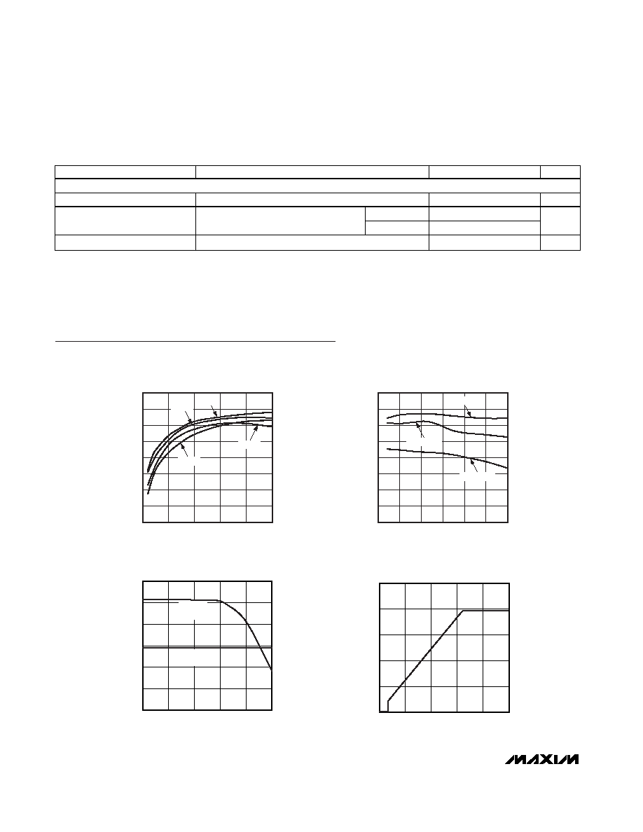
Typical Operating Characteristics
(Circuit of Figure 3, V
IN
= 3.6V, I
LED
= 20mA, 4 LEDs, CTRL = IN, T
A
= +25
°C, unless otherwise noted.)
50
55
60
65
70
75
80
85
90
0
5
10
15
20
25
LED EFFICIENCY vs. I
LED
MAX1578toc01
LED CURRENT (mA)
EFFICIENCY (%)
2 LEDs
4 LEDs
6 LEDs
8 LEDs
50
55
60
65
70
75
80
85
90
2.5
3.0
3.5
4.0
4.5
5.0
5.5
LED EFFICIENCY vs. V
IN
MAX1578toc02
INPUT VOLTAGE (V)
EFFICIENCY (%)
I
LED
= 2mA
I
LED
= 10mA
I
LED
= 20mA
0
10
5
20
15
25
30
-40
85
LED CURRENT vs. TEMPERATURE
MAX1578toc03
TEMPERATURE (
°C)
I
LED
(mA)
10
-15
35
60
MAX1579
R
CS
= 13
MAX1578
R
CS
= 22
0
5
15
10
20
25
0
1.0
0.5
1.5
2.0
2.5
LED CURRENT vs. V
CTRL
MAX1578toc04
CTRL VOLTAGE (V)
I
LED
(mA)
Typical Operating Characteristics (continued)
(Circuit of Figure 3, V
IN
= 3.6V, I
LED
= 20mA, 4 LEDs, CTRL = IN, T
A
= +25
°C, unless otherwise noted.)
MAX1578/MAX1579
Complete Bias and White LED Power Supplies
for Small TFT Displays
_______________________________________________________________________________________
5
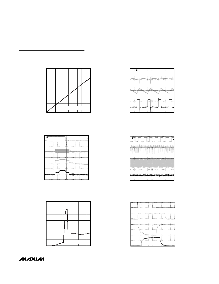
PWM-DIMMING WAVEFORMS
MAX1578toc08
V
CTRL
I
IN
V
OUT
AC-COUPLED
V
IN
AC-COUPLED
2V/div
50mV/div
20mA/div
20mV/div
40
µs/div
0
400
200
800
600
1200
1000
1400
0
2
3
1
4
5
LCD BIAS SUPPLY CURRENT
vs. INPUT VOLTAGE
MAX1578toc09
INPUT VOLTAGE (V)
I
IN
(
µ
A)
V
CTRL
= 0V
LCD BIAS STARTUP SEQUENCE
MAX1578toc10
V
ONBIAS
V
POS
V
NEG
V
MAIN
5V/div
5V/div
10V/div
5V/div
10ms/div
BOOST STARTUP AND
SHUTDOWN WAVEFORMS
MAX1578toc07
V
CTRL
I
IN
V
OUT
V
IN
AC-COUPLED
2V/div
5V/div
0V
100mA/div
20mV/div
4ms/div
0
5
10
15
20
25
0
40 50
20 30
10
60 70 80 90 100
LED CURRENT vs.
DIRECT-PWM DUTY CYCLE
MAX1578toc05
PWM DUTY CYCLE (%)
I
LED
(mA)
f
PWM
= 200Hz TO 200kHz
BOOST-SWITCHING WAVEFORMS
MAX1578toc06
V
IN
AC-COUPLED
V
LX
V
OUT
AC-COUPLED
20mV/div
10V/div
200mV/div
400ns/div