Äîêóìåíòàöèÿ è îïèñàíèÿ www.docs.chipfind.ru
General Description
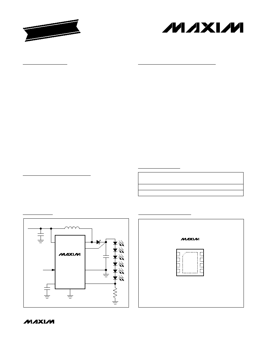
The MAX1561/MAX1599 step-up converters drive up to
six white LEDs with a constant current to provide back-
light in cell phones, PDAs, and other hand-held
devices. The step-up converter topology allows series
connection of the white LEDs so the LED currents are
identical for uniform brightness. This configuration elim-
inates the need for ballast resistors and expensive fac-
tory calibration.
The MAX1561/MAX1599 include an internal, high-volt-
age, low-R
DS(ON)
N-channel MOSFET switch for high
efficiency and maximum battery life. A single Dual
ModeTM input provides a simple means of brightness
adjustment and on/off control. Fast 1MHz (500kHz for
the MAX1599) current-mode, pulse-width modulated
(PWM) operation allows for small input and output
capacitors and a small inductor while minimizing ripple
on the input supply/battery. Programmable soft-start
eliminates inrush current during startup.
Both devices are available in a space-saving, 8-pin 3mm
x 3mm thin DFN package with exposed paddle (EP).
Applications
Cell Phones and Smart Phones
PDAs, Palmtops, and Wireless Handhelds
e-Books and Subnotebooks
White LED Display Backlighting
Features
o Accurate Current Regulation for Uniform
Illumination
o High Efficiency Up to 87%
o Flexible Analog or PWM Dimming Control
o Up to 900mW Output Power with Internal 30V
MOSFET Switch
o Fast 1MHz (MAX1561) or 500kHz (MAX1599) PWM
Operation
o Small, Low-Profile External Components
o 2.6V to 5.5V Input Range
o 26V (max) Output with Overvoltage Protection
o Optimized for Low 15mV
P-P
Input Ripple
o Soft-Start with Zero Inrush Current
o 0.3µA Shutdown Current
o Tiny 8-Pin 3mm x 3mm Thin DFN Package
MAX1561/MAX1599
High-Efficiency, 26V Step-Up Converters
for Two to Six White LEDs
________________________________________________________________ Maxim Integrated Products
1
3mm
× 3mm
THIN DFN
TOP VIEW
1
2
8
7
3
4
6
5
GND
COMP
CS
LX
PGND
IN
CTRL
OUT
MAX1561
MAX1599
PART
TEMP RANGE
PIN-PACKAGE
TOP
MARK
MAX1561ETA
-40
°C to +85°C 8 TDFN-EP*
ACS
MAX1599ETA
-40
°C to +85°C 8 TDFN-EP*
AHG
Pin Configuration
Ordering Information
MAX1561
MAX1599
LX
OUT
PGND
CS
COMP
IN
GND
INPUT 2.6V TO 5.5V
PWM OR
ANALOG
DIMMING
CTRL
OUTPUT UP TO 6 LEDs
Typical Operating Circuit
19-2731; Rev 1; 10/03
For pricing, delivery, and ordering information, please contact Maxim/Dallas Direct! at
1-888-629-4642, or visit Maxim's website at www.maxim-ic.com.
EVALUATION KIT
AVAILABLE
Dual Mode is a trademark of Maxim Integrated Products, Inc.
*EP = Exposed paddle.
MAX1561/MAX1599
High-Efficiency, 26V Step-Up Converters
for Two to Six White LEDs
2
_______________________________________________________________________________________
ABSOLUTE MAXIMUM RATINGS
ELECTRICAL CHARACTERISTICS
(V
IN
= 3V, V
OUT
= 20V, C
OUT
= 0.1µF, C
COMP
= 0.15µF, R
SENSE
= 7.5
, V
CTRL
= 1.5V, Figure 1, T
A
= 0°C to +85°C, unless other-
wise noted. Typical values are at T
A
= +25°C.)
Stresses beyond those listed under "Absolute Maximum Ratings" may cause permanent damage to the device. These are stress ratings only, and functional
operation of the device at these or any other conditions beyond those indicated in the operational sections of the specifications is not implied. Exposure to
absolute maximum rating conditions for extended periods may affect device reliability.
IN to GND .................................................................-0.3V to +6V
PGND to GND .......................................................-0.3V to +0.3V
LX, OUT to GND .....................................................-0.3V to +30V
CTRL to GND...................-0.3V to the lower of +6V or (V
IN
+ 2V)
COMP, CS to GND.........................................-0.3 to (V
IN
+ 0.3V)
I
LX
.............................................................................................1A
Continuous Power Dissipation (T
A
= +70°C)
3mm x 3mm 8-Pin TDFN
(derate 24.4mW/°C above +70°C) .............................1950mW
Operating Temperature Range ...........................-40°C to +85°C
Junction Temperature ......................................................+150°C
Storage Temperature Range .............................-65°C to +150°C
Lead Temperature (soldering, 10s) .................................+300°C
PARAMETER
CONDITIONS
MIN
TYP
MAX
UNITS
Supply Voltage
2.6
5.5
V
UVLO Threshold
V
IN
rising or falling
2.10
2.38
2.55
V
UVLO Hysteresis
40
mV
Quiescent Current
No switching
0.38
0.55
mA
T
A
= +25
°C
0.3
2
Shutdown Supply Current
CTRL = GND, V
OUT
= V
IN
T
A
= +85
°C
1
µA
OVLO Threshold
V
OUT
rising
26
27
29
V
OVLO Hysteresis
2
V
V
OUT
= 26V, V
CTRL
> 0.24V
10
20
30
OUT Input Bias Current
V
OUT
= V
IN
, CTRL = GND
0.01
1
µA
Output Voltage Range
(Note 1)
(V
IN
- V
D1
)
25.5
V
ERROR AMPLIFIER
CTRL to CS Regulation
V
CTRL
= 1V, V
IN
= 2.6V to 5.5V
0.095
0.100
0.105
V
T
A
= +25
°C
0.01
1
CS Input Bias Current
V
CS
= V
CTRL
/10
T
A
= +85
°C
0.03
µA
CTRL Input Resistance
V
CTRL
1.0V
290
500
780
k
CTRL Dual-Mode Threshold
100
170
240
mV
CTRL Dual-Mode Hysteresis
5
mV
MAX1561
6.5
8.2
10.5
CTRL Shutdown Enable Delay
(Note 2)
MAX1599
13.6
16.4
21.0
ms
CS-to-COMP Transconductance
V
COMP
= 1.0V
32
50
82
µS
OSCILLATOR
MAX1561
0.80
1.0
1.25
Operating Frequency
MAX1599
0.4
0.5
0.6
MHz
PWM mode
12
Minimum Duty Cycle
Pulse skipping
0
%
Maximum Duty Cycle
CTRL = IN, CS = GND
91
94
%
MAX1561/MAX1599
High-Efficiency, 26V Step-Up Converters
for Two to Six White LEDs
_______________________________________________________________________________________
3
ELECTRICAL CHARACTERISTICS (continued)
(V
IN
= 3V, V
OUT
= 20V, C
OUT
= 0.1µF, C
COMP
= 0.15µF, R
SENSE
= 7.5
, V
CTRL
= 1.5V, Figure 1, T
A
= 0°C to +85°C, unless other-
wise noted. Typical values are at T
A
= +25°C.)
Note 1: V
D1
is the diode forward-voltage drop of diode D1 in Figure 1.
Note 2: Time from CTRL going below the dual-mode threshold to IC shutdown.
Note 3: Specifications to -40°C are guaranteed by design and not production tested.
PARAMETER
CONDITIONS
MIN
TYP
MAX
UNITS
N-CHANNEL SWITCH
LX On-Resistance
I
LX
= 190mA
1.45
2.25
T
A
= +25
°C
0.01
5
LX Leakage Current
V
LX
= 28V, CTRL = GND
T
A
= +85
°C
1
µA
LX Current Limit
Duty cycle = 90%
450
700
950
mA
ELECTRICAL CHARACTERISTICS
(V
IN
= 3V, V
OUT
= 20V, C
OUT
= 0.1µF, C
COMP
= 0.15µF, R
SENSE
= 7.5
, V
CTRL
= 1.5V, Figure 1, T
A
= -40°C to +85°C, unless other-
wise noted.) (Note 3)
PARAMETER
CONDITIONS
MIN
TYP
MAX
UNITS
Supply Voltage
2.6
5.5
V
UVLO Threshold
V
IN
rising or falling
2.10
2.55
V
Quiescent Current
No switching
0.55
mA
OVLO Threshold
V
OUT
rising
26
29
V
V
OUT
= 26V, V
CTRL
> 0.24V
10
30
OUT Input Bias Current
V
OUT
= V
IN
, CTRL = GND
1
µA
Output Voltage Range
(Note 1)
(V
IN
- V
D1
)
25.5
V
ERROR AMPLIFIER
CTRL to CS Regulation
V
CTRL
= 1V, V
IN
= 2.6V to 5.5V
0.093
0.107
V
CTRL Input Resistance
V
CTRL
1.0V
240
780
k
CTRL Dual-Mode Threshold
100
240
mV
MAX1561
6
11
CTRL Shutdown Enable Delay
(Note 2)
MAX1599
13
22
ms
CS-to-COMP Transconductance
V
COMP
= 1.0V
32
85
µS
OSCILLATOR
MAX1561
0.75
1.25
Operating Frequency
MAX1599
0.37
0.63
MHz
Maximum Duty Cycle
CTRL = IN, CS = GND
91
%
N-CHANNEL SWITCH
LX On-Resistance
2.25
LX Current Limit
Duty cycle = 90%
450
950
mA

MAX1561/MAX1599
High-Efficiency, 26V Step-Up Converters
for Two to Six White LEDs
4
_______________________________________________________________________________________
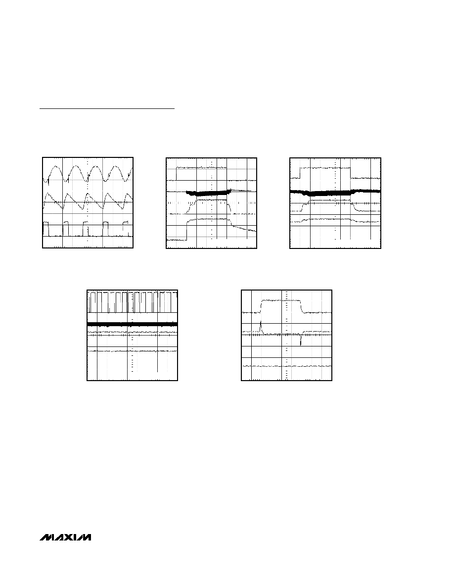
Typical Operating Characteristics
(Circuit of Figure 1, V
IN
= 3.6V, I
LED
= 15mA, L1 = 22µH, C
IN
= 2.2µF, C
OUT
= 0.1µF, C
COMP
= 0.1µF, R
SENSE
= 7.5
, 4 LEDs,
T
A
= +25°C, unless otherwise noted.)
40
60
50
80
70
90
100
0
10
5
15
20
MAX1561
EFFICIENCY vs. LED CURRENT
(vs. NUMBER of LEDs)
MAX1561 toc01
LED CURRENT (mA)
EFFICIENCY (%)
2 LEDs
4 LEDs
6 LEDs
40
60
50
80
70
90
100
0
10
5
15
20
MAX1561
EFFICIENCY vs. LED CURRENT
(vs. INPUT VOLTAGE)
MAX1561 toc02
LED CURRENT (mA)
EFFICIENCY (%)
4.2V
IN
3.6V
IN
2.7V
IN
40
60
50
80
70
90
100
0
10
5
15
20
MAX1561
EFFICIENCY vs. LED CURRENT
(vs. INDUCTANCE)
MAX1561 toc03
LED CURRENT (mA)
EFFICIENCY (%)
10
µH
4.7
µH
47
µH
22
µH
40
60
50
80
70
90
100
0
10
5
15
20
MAX1599 EFFICIENCY vs. LED CURRENT
(vs. NUMBER OF LEDs)
MAX1561 toc04
LED CURRENT (mA)
EFFICIENCY (%)
6 LEDs
2 LEDs
4 LEDs
40
60
50
80
70
90
100
0
10
5
15
20
MAX1599 EFFICIENCY vs. LED CURRENT
(vs. INPUT VOLTAGE)
MAX1561 toc05
LED CURRENT (mA)
EFFICIENCY (%)
2.7V
IN
3.6V
IN
4.2V
IN
40
60
50
80
70
90
100
0
10
5
15
20
MAX1599 EFFICIENCY vs. LED CURRENT
(vs. INDUCTANCE)
MAX1561 toc06
LED CURRENT (mA)
EFFICIENCY (%)
47
µH
22
µH
0
5
10
20
15
25
0
20 30 40 50
10
60 70 80 90 100
LED CURRENT vs. DIRECT-PWM
DIMMING DUTY CYCLE
MAX1561 toc09
DIRECT-PWM DIMMING DUTY CYCLE (%)
LED CURRENT (mA)
V
CTRL
= SQUARE WAVE
200Hz < FREQ < 200kHz
0
10
5
15
30
35
25
20
40
0
10 15 20 25
5
30 35 40 45 50
INPUT RIPPLE vs. INDUCTANCE
MAX1561 toc07
INDUCTANCE (
µH)
INPUT RIPPLE (mV
P-P
)
0
1
2
4
5
3
6
0
2
3
4
5
1
6
7
8
9
10
INPUT RIPPLE SPECTRUM
MAX1561 toc08
FREQUENCY (MHz)
INPUT RIPPLE (mV
RMS
)
MAX1561/MAX1599
High-Efficiency, 26V Step-Up Converters
for Two to Six White LEDs
_______________________________________________________________________________________
5
Typical Operating Characteristics (continued)
(Circuit of Figure 1, V
IN
= 3.6V, I
LED
= 15mA, L1 = 22µH, C
IN
= 2.2µF, C
OUT
= 0.1µF, C
COMP
= 0.1µF, R
SENSE
= 7.5
, 4 LEDs,
T
A
= +25°C, unless otherwise noted.)
SWITCHING WAVEFORMS
MAX1561 toc10
V
IN
10mV/div
V
OUT
100mV/div
V
LX
10V/div
500ns/div
SOFT-START AND SHUTDOWN
MAX1561 toc11
V
CTRL
1V/div
I
IN
50mA/div
V
IN
50mV/div
V
OUT
5V/div
0mA
0V
0V
20ms/div
V
IN
= 3.8V Li+ BATTERY
CTRL STEP RESPONSE
MAX1561 toc12
V
CTRL
1V/div
I
IN
50mA/div
V
IN
50mV/div
V
OUT
5V/div
0mA
0V
0V
20ms/div
V
IN
= 3.8V Li+ BATTERY
DIRECT-PWM DIMMING
MAX1561 toc13
V
CTRL
32kHz
1V/div
I
IN
50mA/div
V
IN
50mV/div
V
OUT
5V/div
0mA
0V
0V
50
µs/div
V
IN
= 3.8V Li+ BATTERY
LINE-TRANSIENT RESPONSE
MAX1561 toc14
V
IN
500mV/div
I
IN
50mA/div
V
CS
100mV/div
0V
3.5V
4V
0mA
50
µs/div