Äîêóìåíòàöèÿ è îïèñàíèÿ www.docs.chipfind.ru
For free samples and the latest literature, visit www.maxim-ic.com or phone 1-800-998-8800.
For small orders, phone 1-800-835-8769.
MAX1282/MAX1283
300ksps/400ksps, Single-Supply, 4-Channel,
Serial 12-Bit ADCs with Internal Reference
________________________________________________________________ Maxim Integrated Products
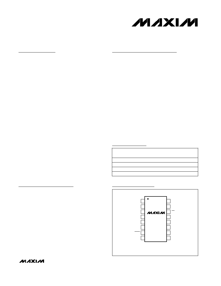
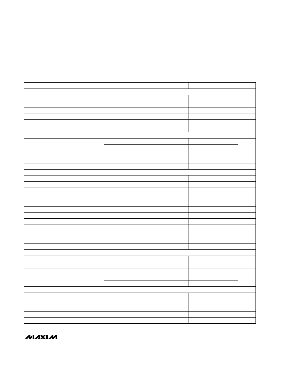
1
16
15
14
13
12
11
10
9
1
2
3
4
5
6
7
8
V
DD1
V
DD2
SCLK
DIN
SSTRB
CS
DOUT
GND
REFADJ
TOP VIEW
MAX1282/
MAX1283
TSSOP
CH0
CH1
COM
CH2
CH3
SHDN
REF
19-1688; Rev 0; 5/00
Typical Operating Circuit appears at end of data sheet.
Pin Configuration
Ordering Information
SPI and QSPI are trademarks of Motorola, Inc.
MICROWIRE is a trademark of National Semiconductor Corp.
General Description
The MAX1282/MAX1283 12-bit analog-to-digital convert-
ers (ADCs) combine a 4-channel analog-input multiplexer,
high-bandwidth track/hold (T/H), and serial interface with
high conversion speed and low power consumption. The
MAX1282 operates from a single +4.5V to +5.5V supply;
the MAX1283 operates from a single +2.7V to +3.6V sup-
ply. Both devices' analog inputs are software configurable
for unipolar/bipolar and single-ended/pseudo-differential
operation.
The 4-wire serial interface connects directly to
SPITM/QSPITM/MICROWIRETM devices without external
logic. A serial strobe output allows direct connection to
TMS320-family digital signal processors. The MAX1282/
MAX1283 use an external serial-interface clock to perform
successive-approximation analog-to-digital conversions.
The devices feature an internal +2.5V reference and a ref-
erence-buffer amplifier with a ±1.5% voltage-adjustment
range. An external reference with a 1V to V
DD
range may
also be used.
The MAX1282/MAX1283 provide a hardwired SHDN pin
and four software-selectable power modes (normal opera-
tion, reduced power (REDP), fast power-down (FASTPD),
and full power-down (FULLPD)). These devices can be
programmed to automatically shut down at the end of a
conversion or to operate with reduced power. When using
the power-down modes, accessing the serial interface
automatically powers up the devices, and the quick turn-
on time allows them to be shut down between all conver-
sions.
The MAX1282/MAX1283 are available in 16-pin TSSOP
packages.
Applications
Portable Data Logging
Data Acquisition
Medical Instruments
Battery-Powered Instruments
Pen Digitizers
Process Control
Features
o 4-Channel Single-Ended or 2-Channel
Pseudo-Differential Inputs
o Internal Multiplexer and Track/Hold
o Single-Supply Operation
+4.5V to +5.5V (MAX1282)
+2.7V to +3.6V (MAX1283)
o Internal +2.5V Reference
o 400kHz Sampling Rate (MAX1282)
o Low Power: 2.5mA (400ksps)
1.3mA (REDP)
0.9mA (FASTPD)
2µA (FULLPD)
o SPI/QSPI/MICROWIRE/TMS320-Compatible 4-Wire
Serial Interface
o Software-Configurable Unipolar or Bipolar Inputs
o 16-Pin TSSOP Package
±1
16 TSSOP
0°C to +70°C
MAX1283BCUE
±1
16 TSSOP
-40°C to +85°C
MAX1283BEUE
±1
16 TSSOP
-40°C to +85°C
MAX1282BEUE
INL
(LSB)
PIN-
PACKAGE
TEMP.
RANGE
PART
±1
16 TSSOP
0°C to +70°C
MAX1282BCUE
MAX1282/MAX1283
300ksps/400ksps, Single-Supply, 4-Channel,
Serial 12-Bit ADCs with Internal Reference
2
_______________________________________________________________________________________
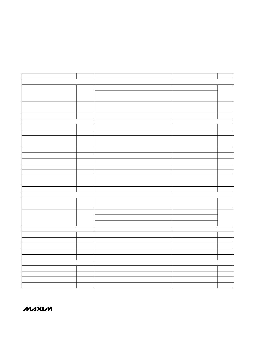
ABSOLUTE MAXIMUM RATINGS
ELECTRICAL CHARACTERISTICS--MAX1282
(V
DD1
= V
DD2
= +4.5V to +5.5V, COM = GND, f
OSC
= 6.4MHz, 50% duty cycle, 16 clocks/conversion cycle (400ksps), external
+2.5V at REF, REFADJ = V
DD1
, T
A
= T
MIN
to T
MAX
, unless otherwise noted. Typical values are at T
A
= +25°C.)
Stresses beyond those listed under "Absolute Maximum Ratings" may cause permanent damage to the device. These are stress ratings only, and functional
operation of the device at these or any other conditions beyond those indicated in the operational sections of the specifications is not implied. Exposure to
absolute maximum rating conditions for extended periods may affect device reliability.
V
DD
_ to GND ........................................................... -0.3V to +6V
V
DD1
to V
DD2
....................................................... -0.3V to +0.3V
CH0CH3, COM to GND .......................... -0.3V to (V
DD
_ +0.3V)
REF, REFADJ to GND ................................ -0.3V to V
DD
_ +0.3V)
Digital Inputs to GND .............................................. -0.3V to +6V
Digital Outputs to GND............................. -0.3V to (V
DD
_ +0.3V)
Digital Output Sink Current .................................................25mA
Continuous Power Dissipation (T
A
= +70°C)
16-Pin TSSOP (derate 6.7mW/°C above +70°C) ........ 535mW
Operating Temperature Ranges
MAX1282BCUE/MAX1283BCUE ....................... 0°C to +70°C
MAX1282BEUE/MAX1283BEUE ..................... -40°C to +85°C
Storage Temperature Range ............................ -60°C to +150°C
Lead Temperature (soldering, 10s) ................................ +300°C
SINAD > 68dB
-3dB point
200kHz, V
IN
= 2.5Vp-p
f
IN1
= 99kHz, f
IN2
=102kHz
No missing codes over temperature
Up to the 5th harmonic
CONDITIONS
MHz
0.5
6.4
f
SCLK
Serial Clock Frequency
ps
<50
Aperture Jitter
ns
10
Aperture Delay
ns
400
t
ACQ
Track/Hold Acquisition Time
µs
2.5
t
CONV
Conversion Time (Note 5)
kHz
350
Full-Linear Bandwidth
MHz
6
Full-Power Bandwidth
dB
-78
Channel-to-Channel Crosstalk
(Note 4)
dB
76
IMD
Intermodulation Distortion
dB
80
SFDR
Spurious-Free Dynamic Range
dB
-81
THD
Total Harmonic Distortion
Bits
12
Resolution
dB
70
SINAD
Signal-to-Noise plus Distortion
Ratio
LSB
±0.2
Channel-to-Channel Offset-Error
Matching
ppm/°C
±1.6
Gain-Error Temperature
Coefficient
±1.0
LSB
±1.0
DNL
Differential Nonlinearity
LSB
±6.0
Offset Error
LSB
±6.0
Gain Error (Note 3)
UNITS
MIN
TYP
MAX
SYMBOL
PARAMETER
%
40
60
Duty Cycle
DYNAMIC SPECIFICATIONS (100kHz sine-wave input, 2.5Vp-p, 400ksps, 6.4MHz clock, bipolar input mode)
DC ACCURACY (Note 1)
CONVERSION RATE
LSB
INL
Relative Accuracy (Note 2)
MAX1282/MAX1283
300ksps/400ksps, Single-Supply, 4-Channel,
Serial 12-Bit ADCs with Internal Reference
_______________________________________________________________________________________
3
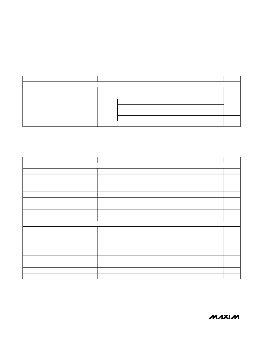
ELECTRICAL CHARACTERISTICS--MAX1282 (continued)
(V
DD1
= V
DD2
= +4.5V to +5.5V, COM = GND, f
OSC
= 6.4MHz, 50% duty cycle, 16 clocks/conversion cycle (400ksps), external
+2.5V at REF, REFADJ = V
DD1
, T
A
= T
MIN
to T
MAX
, unless otherwise noted. Typical values are at T
A
= +25°C.)
CONDITIONS
UNITS
MIN
TYP
MAX
SYMBOL
PARAMETER
To power down the internal reference
For small adjustments, from 1.22V
0 to 1mA output load
On/off leakage current, V
COM
, V
CH_
= 0 or
V
DD1
T
A
= +25°C
Bipolar, V
COM
or V
CH_
= V
REF
/2, referenced
to COM or CH_
Unipolar, V
COM
= 0
V/V
+2.05
Buffer Voltage Gain
V
1.4
V
DD1
- 1.0
REFADJ Buffer Disable
Threshold
mV
±100
REFADJ Input Range
V
1.22
REFADJ Output Voltage
µF
0.01
10
Capacitive Bypass at REFADJ
µF
4.7
10
Capacitive Bypass at REF
mV/mA
0.05
2.0
Load Regulation (Note 7)
ppm/°C
±15
TC V
REF
REF Output Temperature
Coefficient
mA
15
REF Short-Circuit Current
V
2.480
2.500
2.520
V
REF
REF Output Voltage
pF
18
Input Capacitance
µA
±0.001
±1
Multiplexer Leakage Current
±V
REF
/2
V
V
REF
V
CH_
Input Voltage Range, Single-
Ended and Differential (Note 6)
V
IN
= 0 or V
DD2
In full power-down mode, f
SCLK
= 0
V
REF
= 2.500V, f
SCLK
= 0
V
REF
= 2.500V, f
SCLK
= f
MAX
(Note 8)
pF
C
IN
Input Capacitance
µA
±1
I
IN
Input Leakage
V
0.2
V
HYST
Input Hysteresis
V
0.8
V
INL
Input Low Voltage
V
3.0
V
INH
Input High Voltage
5
320
µA
200
350
REF Input Current
V
1.0
V
DD1
+
50mV
REF Input Voltage Range
I
SINK
= 5mA
V
0.4
V
OL
Output Voltage Low
15
I
SOURCE
= 1mA
V
4
V
OH
Output Voltage High
CS = V
DD2
µA
±10
I
L
Three-State Leakage Current
CS = V
DD2
pF
15
C
OUT
Three-State Output Capacitance
ANALOG INPUTS (CH3CH0, COM)
EXTERNAL REFERENCE (reference buffer disabled, reference applied to REF)
INTERNAL REFERENCE
DIGITAL INPUTS (DIN, SCLK, CS, SHDN)
DIGITAL OUTPUTS (DOUT, SSTRB)
MAX1282/MAX1283
300ksps/400ksps, Single-Supply, 4-Channel,
Serial 12-Bit ADCs with Internal Reference
4
_______________________________________________________________________________________
V
DD1
=
V
DD2
=
5.5V
V
DD1
= V
DD2
= 5V ±10%, midscale input
CONDITIONS
mA
2.5
4.0
IV
DD1
+
IV
DD2
Supply Current
V
4.5
5.5
V
DD1,
V
DD2
Positive Supply Voltage
(Note 9)
1.3
2.0
0.9
1.5
µA
2.0
10
mV
±0.5
±2.0
PSR
Power-Supply Rejection
UNITS
MIN
TYP
MAX
SYMBOL
PARAMETER
Normal operating mode (Note 10)
Reduced-power mode (Note 11)
Fast power-down mode (Note 11)
Full power-down mode (Note 11)
ELECTRICAL CHARACTERISTICS--MAX1282 (continued)
(V
DD1
= V
DD2
= +4.5V to +5.5V, COM = GND, f
OSC
= 6.4MHz, 50% duty cycle, 16 clocks/conversion cycle (400ksps), external
+2.5V at REF, REFADJ = V
DD1
, T
A
= T
MIN
to T
MAX
, unless otherwise noted. Typical values are at T
A
= +25°C.)
ELECTRICAL CHARACTERISTICS--MAX1283
(V
DD1
= V
DD2
= +2.7V to +3.6V, COM = GND, f
OSC
= 4.8MHz, 50% duty cycle, 16 clocks/conversion cycle (300ksps), external
+2.5V at REF, REFADJ = V
DD1
, T
A
= T
MIN
to T
MAX
, unless otherwise noted. Typical values are at T
A
= +25°C.)
SINAD > 68dB
-3dB point
f = 150kHz, V
IN
= 2.5Vp-p
f
IN1
= 73kHz, f
IN2
= 77kHz
No missing codes over temperature
Up to the 5th harmonic
CONDITIONS
kHz
250
Full-Linear Bandwidth
MHz
3
Full-Power Bandwidth
dB
-78
Channel-to-Channel Crosstalk
(Note 4)
dB
76
IMD
Intermodulation Distortion
dB
72
SFDR
Spurious-Free Dynamic Range
dB
-70
THD
Total Harmonic Distortion
Bits
12
Resolution
dB
70
SINAD
Signal-to-Noise plus Distortion
Ratio
LSB
±0.2
Channel-to-Channel Offset-Error
Matching
ppm/°C
±1.6
Gain-Error Temperature
Coefficient
±1.0
LSB
±1.0
DNL
Differential Nonlinearity
LSB
±6.0
Offset Error
LSB
±6.0
Gain Error (Note 3)
UNITS
MIN
TYP
MAX
SYMBOL
PARAMETER
POWER SUPPLY
LSB
INL
Relative Accuracy (Note 2)
DC ACCURACY (Note 1)
DYNAMIC SPECIFICATIONS (100kHz sine-wave input, 2.5Vp-p, 400ksps, 6.4MHz clock, bipolar input mode)
MAX1282/MAX1283
300ksps/400ksps, Single-Supply, 4-Channel,
Serial 12-Bit ADCs with Internal Reference
_______________________________________________________________________________________
5
ELECTRICAL CHARACTERISTICS--MAX1283 (continued)
(V
DD1
= V
DD2
= +2.7V to +3.6V, COM = GND, f
OSC
= 4.8MHz, 50% duty cycle, 16 clocks/conversion cycle (300ksps), external
+2.5V at REF, REFADJ = V
DD1
, T
A
= T
MIN
to T
MAX
, unless otherwise noted. Typical values are at T
A
= +25°C.)
Normal operating mode
Normal operating mode
Normal operating mode
CONDITIONS
MHz
0.5
4.8
f
SCLK
Serial Clock Frequency
ps
<50
Aperture Jitter
ns
10
Aperture Delay
ns
625
t
ACQ
Track/Hold Acquisition Time
µs
3.3
t
CONV
Conversion Time (Note 5)
UNITS
MIN
TYP
MAX
SYMBOL
PARAMETER
To power down the internal reference
For small adjustments, from 1.22V
0 to 0.75mA output load
On/off leakage current, V
CH_
= 0 or V
DD1
T
A
= +25°C
Bipolar, V
COM
or V
CH_
= V
REF
/2,
referenced to COM or CH_
Unipolar, V
COM
= 0
V/V
2.05
Buffer Voltage Gain
V
1.4
V
DD1
- 1.0
REFADJ Buffer Disable
Threshold
mV
±100
REFADJ Input Range
V
1.22
REFADJ Output Voltage
µF
0.01
10
Capacitive Bypass at REFADJ
µF
4.7
10
Capacitive Bypass at REF
mV/mA
0.1
2.0
Load Regulation (Note 7)
ppm/°C
±15
TC V
REF
REF Output Temperature
Coefficient
mA
15
REF Short-Circuit Current
V
2.480
2.500
2.520
V
REF
REF Output Voltage
pF
18
Input Capacitance
µA
±0.001
±1
Multiplexer Leakage Current
±V
REF
/2
%
40
60
Duty Cycle
V
V
REF
V
CH_
Input Voltage Range, Single
Ended and Differential (Note 6)
V
IN
= 0 or V
DD2
In full power-down mode, f
SCLK
= 0
V
REF
= 2.500V, f
SCLK
= 0
V
REF
= 2.500V, f
SCLK
= f
MAX
(Note 8)
pF
15
C
IN
Input Capacitance
µA
±1
I
IN
Input Leakage
V
0.2
V
HYST
Input Hysteresis
V
0.8
V
INL
Input Low Voltage
V
2.0
V
INH
Input High Voltage
5
REF Input Current
320
µA
200
350
V
1.0
V
DD1
+
50mV
REF Input Voltage Range
V/V
2.05
Buffer Voltage Gain
CONVERSION RATE
ANALOG INPUTS (CH3CH0, COM)
INTERNAL REFERENCE
EXTERNAL REFERENCE (reference buffer disabled, reference applied to REF)
DIGITAL INPUTS (DIN, SCLK, CS, SHDN)