Äîêóìåíòàöèÿ è îïèñàíèÿ www.docs.chipfind.ru
General Description
The MAX1265/MAX1267 low-power, 12-bit analog-to-
digital converters (ADCs) feature a successive-approxi-
mation ADC, automatic power-down, fast wake-up
(2µs), an on-chip clock, +2.5V internal reference, and a
high-speed 12-bit parallel interface. They operate with
a single +2.7V to +3.6V analog supply.
Power consumption is only 5.4mW at the maximum
sampling rate of 265ksps. Two software-selectable
power-down modes enable the MAX1265/MAX1267 to
be shut down between conversions; accessing the par-
allel interface returns them to normal operation.
Powering down between conversions can reduce sup-
ply current below 10µA at lower sampling rates.
Both devices offer software-configurable analog inputs
for unipolar/bipolar and single-ended/pseudo-differen-
tial operation. In single-ended mode, the MAX1265 has
six input channels and the MAX1267 has two (three
input channels and one input channel, respectively,
when in pseudo-differential mode).
Excellent dynamic performance and low power, com-
bined with ease of use and small package size, make
these converters ideal for battery-powered and data-
acquisition applications or for other circuits with demand-
ing power-consumption and space requirements. The
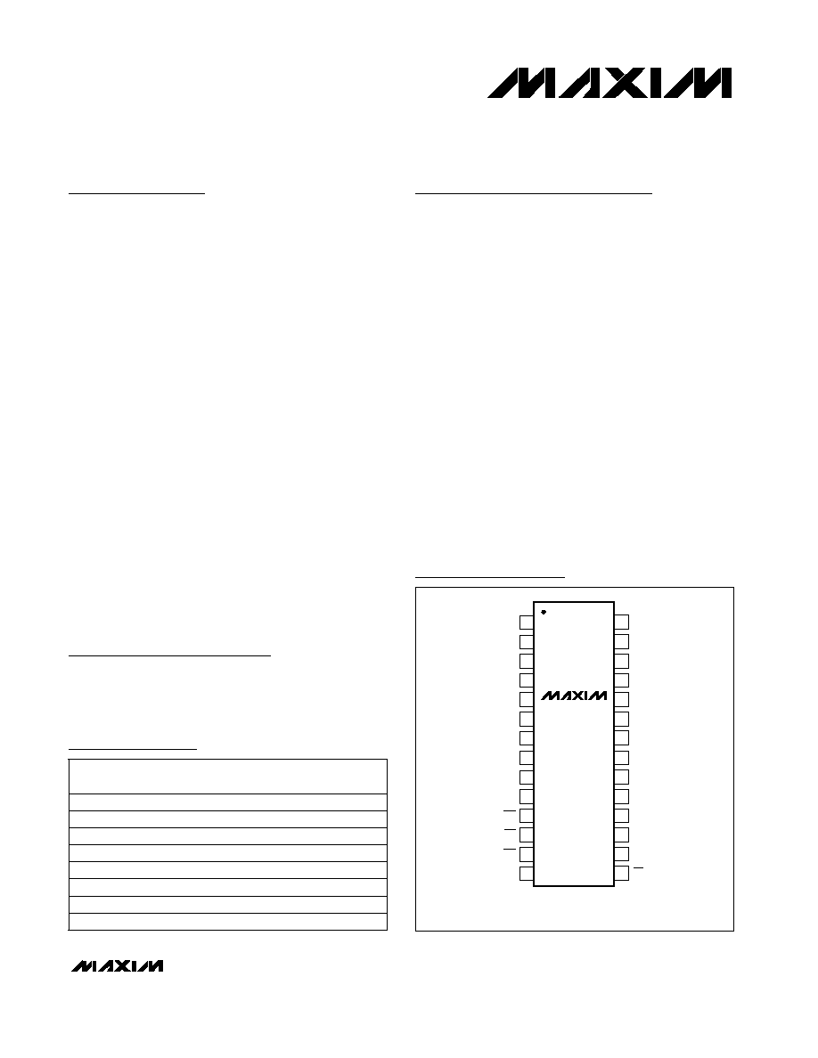
MAX1265 is offered in a 28-pin QSOP package, while the
MAX1267 comes in a 24-pin QSOP. For pin-compatible
+5V, 12-bit versions, refer to the MAX1266/MAX1268
data sheet.
Applications
Industrial Control Systems
Data Logging
Energy Management
Patient Monitoring
Data-Acquisition Systems
Touch Screens
Features
o 12-Bit Resolution, ±0.5 LSB Linearity
o +3V Single-Supply Operation
o Internal +2.5V Reference
o Software-Configurable Analog Input Multiplexer
6-Channel Single Ended/
3-Channel Pseudo Differential (MAX1265)
2-Channel Single Ended/
1-Channel Pseudo Differential (MAX1267)
o Software-Configurable Unipolar/Bipolar
Analog Inputs
o Low Current
1.9mA (265ksps)
1.0mA (100ksps)
400µA (10ksps)
2µA (Shutdown)
o Internal 3MHz Full-Power Bandwidth Track/Hold
o Parallel 12-Bit Interface
o Small Footprint
28-Pin QSOP (MAX1265)
24-Pin QSOP (MAX1267)
MAX1265/MAX1267
265ksps, +3V, 6-/2-Channel, 12-Bit ADCs
with +2.5V Reference and Parallel Interface
________________________________________________________________ Maxim Integrated Products
1
19-2721; Rev 0; 04/03
28 QSOP
±1
0°C to +70°C
MAX1265BCEI
INL
(LSB)
±0.5
28 QSOP
PIN-PACKAGE
TEMP RANGE
0°C to +70°C
MAX1265ACEI
PART
Ordering Information
Pin Configurations
Typical Operating Circuits appear at end of data sheet.
28
27
26
25
24
23
22
21
20
19
18
17
16
15
1
2
3
4
5
6
7
8
9
10
11
12
13
14
D10
D11
V
DD
REF
REFADJ
GND
CS
COM
CH0
CH1
CH2
CH3
CH4
CH5
CLK
WR
RD
INT
D0
D1
D2
D3
D4
D5
D6
D7
D8
D9
QSOP
TOP VIEW
MAX1265
Pin Configurations continued at end of data sheet.
28 QSOP
±0.5
-40°C to +85°C
MAX1265AEEI
28 QSOP
±1
-40°C to +85°C
MAX1265BEEI
24 QSOP
±0.5
-40°C to +85°C
MAX1267AEEG
24 QSOP
±1
-40°C to +85°C
MAX1267BEEG
24 QSOP
±1
0°C to +70°C
MAX1267BCEG
±0.5
24 QSOP
0°C to +70°C
MAX1267ACEG
For pricing, delivery, and ordering information, please contact Maxim/Dallas Direct! at
1-888-629-4642, or visit Maxim's website at www.maxim-ic.com.
MAX1265/MAX1267
265ksps, +3V, 6-/2-Channel, 12-Bit ADCs
with +2.5V Reference and Parallel Interface
2
_______________________________________________________________________________________
ABSOLUTE MAXIMUM RATINGS
ELECTRICAL CHARACTERISTICS
(V
DD
= +2.7V to +3.6V, COM = GND, REFADJ = V
DD
, V
REF
= +2.5V, 4.7µF capacitor at REF pin, f
CLK
= 4.8MHz (50% duty cycle),
T
A
= T
MIN
to T
MAX
, unless otherwise noted. Typical values are at T
A
= +25°C.)
Stresses beyond those listed under "Absolute Maximum Ratings" may cause permanent damage to the device. These are stress ratings only, and functional
operation of the device at these or any other conditions beyond those indicated in the operational sections of the specifications is not implied. Exposure to
absolute maximum rating conditions for extended periods may affect device reliability.
V
DD
to GND ..............................................................-0.3V to +6V
CH0CH5, COM to GND ............................-0.3V to (V
DD
+ 0.3V)
REF, REFADJ to GND.................................-0.3V to (V
DD
+ 0.3V)
Digital Inputs to GND ...............................................-0.3V to +6V
Digital Outputs (D0D11, INT) to GND.......-0.3V to (V
DD
+ 0.3V)
Continuous Power Dissipation (T
A
= +70°C)
24-Pin QSOP (derate 9.5mW/°C above +70°C)..........762mW
28-Pin QSOP (derate 8.0mW/°C above +70°C)..........667mW
Operating Temperature Ranges
MAX1265_C_ _ /MAX1267_C_ _ ........................0°C to +70°C
MAX1265_E_ _ /MAX1267_E_ _ ......................-40°C to +85°C
Storage Temperature Range .............................-65°C to +150°C
Lead Temperature (soldering, 10s) .................................+300°C
External acquisition or external clock mode
Internal acquisition/internal clock mode
MAX126_A
External acquisition/internal clock mode
External clock mode
-3dB rolloff
SINAD > 68dB
f
IN
= 125kHz (Note 4)
f
IN1
= 49kHz, f
IN2
= 52kHz
MAX126_B
No missing codes overtemperature
(Note 3)
CONDITIONS
ns
50
Aperture Delay
ns
625
t
ACQ
Track/Hold Acquisition Time
3.2
3.6
4.1
2.5
3.0
3.5
µs
3.3
t
CONV
Conversion Time (Note 5)
MHz
3
Full-Power Bandwidth
kHz
250
Full-Linear Bandwidth
dB
-78
Channel-to-Channel Crosstalk
dB
76
IMD
Intermodulation Distortion
dB
80
SFDR
Spurious-Free Dynamic Range
dB
Total Harmonic Distortion
(Including 5th-Order Harmonic)
-78
THD
±0.5
INL
Relative Accuracy (Note 2)
Bits
12
RES
Resolution
dB
67
70
SINAD
Signal-to-Noise Plus Distortion
LSB
±0.2
Channel-to-Channel Offset
Matching
ppm/°C
±2.0
Gain Temperature Coefficient
LSB
±1
LSB
±1
DNL
Differential Nonlinearity
LSB
±4
Offset Error
LSB
±4
Gain Error
UNITS
MIN
TYP
MAX
SYMBOL
PARAMETER
Internal acquisition/internal clock mode
External acquisition or external clock mode
<200
ps
<50
Aperture Jitter
MHz
0.1
4.8
f
CLK
External Clock Frequency
%
30
70
Duty Cycle
DC ACCURACY (Note 1)
DYNAMIC SPECIFICATIONS (f
IN(sine-wave)
= 50kHz, V
IN
= 2.5V
P-P
, 265ksps, external f
CLK
= 4.8MHz, bipolar input mode)
CONVERSION RATE
MAX1265/MAX1267
265ksps, +3V, 6-/2-Channel, 12-Bit ADCs
with +2.5V Reference and Parallel Interface
_______________________________________________________________________________________
3
ELECTRICAL CHARACTERISTICS (continued)
(V
DD
= +2.7V to +3.6V, COM = GND, REFADJ = V
DD
, V
REF
= +2.5V, 4.7µF capacitor at REF pin, f
CLK
= 4.8MHz (50% duty cycle),
T
A
= T
MIN
to T
MAX
, unless otherwise noted. Typical values are at T
A
= +25°C.)
CONDITIONS
UNITS
MIN
TYP
MAX
SYMBOL
PARAMETER
0 to 0.5mA output load
To power down the internal reference
For small adjustments
On-/off-leakage current, V
IN
= 0 or V
DD
Unipolar, V
COM
= 0
bipolar, V
COM
= V
REF
/ 2
V
1.0
V
DD
+
50mV
V
REF
REF Input Voltage Range
µF
4.7
10
Capacitive Bypass at REF
µF
0.01
1
Capacitive Bypass at REFADJ
mV/mA
0.2
Load Regulation (Note 7)
V
V
DD
- 1
REFADJ High Threshold
mV
±100
REFADJ Input Range
mA
15
REF Short-Circuit Current
V
2.49
2.5
2.51
REF Output Voltage
pF
12
C
IN
Input Capacitance
µA
±0.01
±1
Multiplexer Leakage Current
V
Analog Input Voltage Range
Single Ended and Differential
(Note 6)
0 V
REF
- V
REF
/2
+ V
REF
/2
V
IN
CS = V
DD
I
SOURCE
= 1mA
I
SINK
= 1.6mA
V
IN
= 0 or V
DD
V
REF
= 2.5V, f
SAMPLE
= 265ksps
µA
±0.1
±1
I
LEAKAGE
Tri-State Leakage Current
V
V
DD
- 0.5
V
OH
Output Voltage High
V
0.4
V
OL
Output Voltage Low
pF
15
C
IN
Input Capacitance
µA
±0.1
±1
I
IN
Input Leakage Current
mV
200
V
HYS
Input Hysteresis
V
0.8
V
IL
Input Voltage Low
V
2.0
V
IH
Input Voltage High
µA
200
300
I
REF
REF Input Current
CS = V
DD
V
2.7
3.6
V
DD
Analog Supply Voltage
pF
15
C
OUT
Tri-State Output Capacitance
Internal reference
2.5
2.8
ppm/°C
±20
TC
REF
REF Temperature Coefficient
Shutdown mode
2
External reference
1.9
2.3
0.9
1.2
Positive Supply Current
Shutdown mode
2
10
µA
Power-Supply Rejection
PSR
V
DD
= 2.7V to 3.6V, full-scale input
±0.4
±0.9
mV
I
DD
0.5
0.8
mA
Operating mode,
f
SAMPLE
= 265ksps
Internal reference
External reference
Standby mode
CONVERSION RATE (continued)
ANALOG INPUTS
INTERNAL REFERENCE
EXTERNAL REFERENCE AT REF
DIGITAL INPUTS AND OUTPUTS
POWER REQUIREMENTS
MAX1265/MAX1267
265ksps, +3V, 6-/2-Channel, 12-Bit ADCs
with +2.5V Reference and Parallel Interface
4
_______________________________________________________________________________________
t
TR
20
70
ns
C
LOAD
= 20pF, Figure 1
RD Rise to Output Disable
WR to CLK Fall Setup Time
t
CWS
40
ns
ns
CLK Pulse Width High
ns
CLK Period
t
CH
40
RD Fall to Output Data Valid
t
DO
20
70
ns
RD Fall to INT High Delay
t
INT1
100
ns
CS Fall to Output Data Valid
t
DO2
110
ns
C
LOAD
= 20pF, Figure 1
C
LOAD
= 20pF, Figure 1
C
LOAD
= 20pF, Figure 1
t
CP
208
CLK Pulse Width Low
t
CL
40
ns
Data Valid to WR Rise Time
t
DS
40
ns
WR Rise to Data Valid Hold Time
t
DH
0
ns
CLK Fall to WR Hold Time
t
CWH
40
ns
CS to CLK or WR Setup Time
t
CSWS
60
ns
CLK or WR to CS Hold Time
t
CSWH
0
ns
CS Pulse Width
t
CS
100
ns
WR Pulse Width
t
WR
60
ns
t
TC
20
100
ns
(Note 8)
C
LOAD
= 20pF, Figure 1
PARAMETER
SYMBOL
MIN
TYP
MAX
UNITS
CONDITIONS
CS Rise to Output Disable
Note 1: Tested at V
DD
= +3V, COM = GND, unipolar single-ended input mode.
Note 2: Relative accuracy is the deviation of the analog value at any code from its theoretical value after offset and gain errors have
been removed.
Note 3: Offset nulled.
Note 4: On channel is grounded; sine wave applied to off channels.
Note 5: Conversion time is defined as the number of clock cycles times the clock period; clock has a 50% duty cycle.
Note 6: Input voltage range referenced to negative input. The absolute range for the analog inputs is from GND to V
DD
.
Note 7: External load should not change during conversion for specified accuracy.
Note 8: When bit 5 is set low for internal acquisition, WR must not return low until after the first falling clock edge of the conversion.
TIMING CHARACTERISTICS
(V
DD
= +2.7V to +3.6V, COM = GND, REFADJ = V
DD
, V
REF
= +2.5V, 4.7µF capacitor at REF pin, f
CLK
= 4.8MHz (50% duty cycle),
T
A
= T
MIN
to T
MAX
, unless otherwise noted. Typical values are at T
A
= +25°C.)
6k
3k
DOUT
DOUT
V
DD
a) HIGH-Z TO V
OH
AND V
OL
TO V
OH
b) HIGH-Z TO V
OL
AND V
OH
TO V
OL
C
LOAD
20pF
C
LOAD
20pF
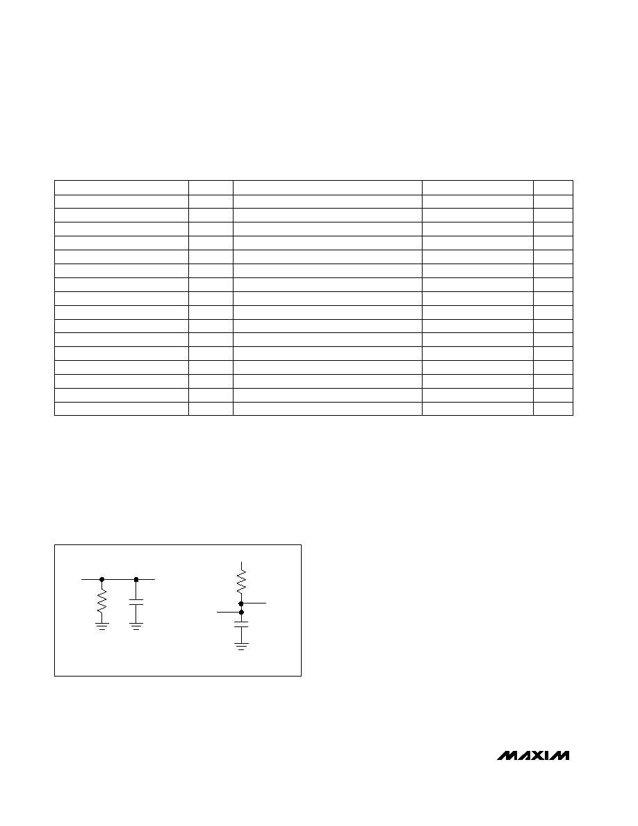
Figure 1. Load Circuits for Enable/Disable Times
MAX1265/MAX1267
265ksps, +3V, 6-/2-Channel, 12-Bit ADCs
with +2.5V Reference and Parallel Interface
_______________________________________________________________________________________
5
-0.5
-0.2
-0.3
-0.4
-0.1
0
0.1
0.2
0.3
0.4
0.5
0
2000
1000
3000
4000
5000
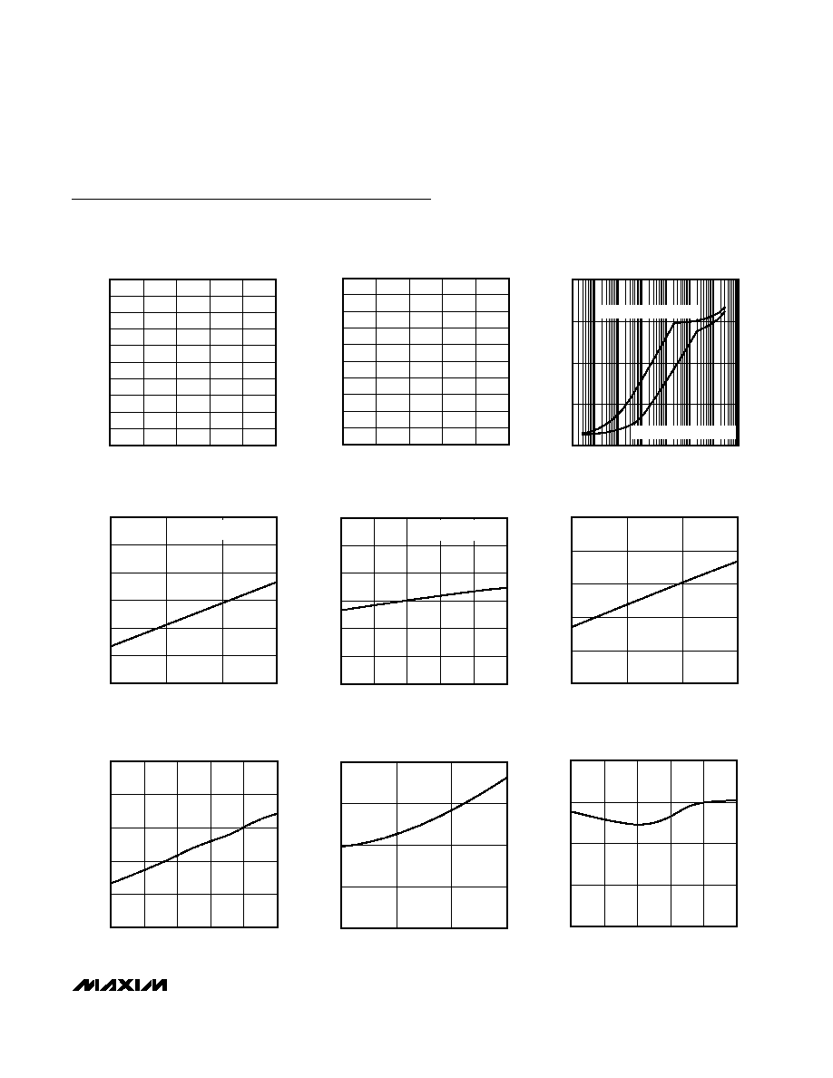
INTEGRAL NONLINEARITY
vs. DIGITAL OUTPUT CODE
MAX1265/67 toc01
DIGITAL OUTPUT CODE
INL (LSB)
-0.5
-0.2
-0.3
-0.4
-0.1
0
0.1
0.2
0.3
0.4
0.5
0
2000
1000
3000
4000
5000
DIFFERENTIAL NONLINEARITY
vs. DIGITAL OUTPUT CODE
MAX1265/67 toc02A
DIGITAL OUTPUT CODE
DNL (LSB)
1.80
1.90
1.85
2.00
1.95
2.05
2.10
2.7
3.0
3.3
3.6
SUPPLY CURRENT vs. SUPPLY VOLTAGE
MAX1265/67 toc03
V
DD
(V)
I
DD
(mA)
R
L
=
CODE = 101010100000
1.6
1.8
1.7
2.0
1.9
2.1
2.2
-40
10
-15
35
60
85
SUPPLY CURRENT vs. TEMPERATURE
MAX1265/67 toc04
TEMPERATURE (
°C)
I
DD
(mA)
R
L
=
CODE = 101010100000
880
890
910
900
920
930
STANDBY CURRENT vs. SUPPLY VOLTAGE
MAX1265/67 toc05
V
DD
(V)
STANDBY I
DD
(
µ
A)
2.7
3.3
3.0
3.6
880
890
910
900
920
930
STANDBY CURRENT
vs. TEMPERATURE
MAX1265/67 toc06
TEMPERATURE (
°C)
STANDBY I
DD
(
µ
A)
-40
10
-15
35
85
60
0.50
1.00
0.75
1.25
1.50
2.7
3.0
3.3
3.6
POWER-DOWN CURRENT
vs. SUPPLY VOLTAGE
MAX1265/67 toc07
V
DD
(V)
POWER-DOWN I
DD
(
µ
A)
0.8
0.9
1.0
1.1
1.2
POWER-DOWN CURRENT
vs. TEMPERATURE
MAX1265/67 toc08
TEMPERATURE (
°C)
POWER-DOWN I
DD
(
µ
A)
-40
35
-15
10
60
85
Typical Operating Characteristics
(V
DD
= +3V, V
REF
= +2.500V, f
CLK
= 4.8MHz, C
L
= 20pF, T
A
= +25°C, unless otherwise noted.)
0.1
1k
100k
10
1
100
10k
1M
SUPPLY CURRENT
vs. SAMPLE FREQUENCY
MAX1265/67 toc02B
f
SAMPLE
(Hz)
I
DD
(
µ
A)
0
10
100
1000
10,000
WITH EXTERNAL REFERENCE
WITH INTERNAL REFERENCE