Äîêóìåíòàöèÿ è îïèñàíèÿ www.docs.chipfind.ru
________________General Description
The MAX115/MAX116 are high-speed, multichannel,
12-bit data-acquisition systems (DAS) with simultane-
ous track/holds (T/Hs). These devices contain a 12-bit,
2µs, successive-approximation analog-to-digital con-
verter (ADC), a +2.5V reference, a buffered reference
input, and a bank of four simultaneous-sampling T/H
amplifiers that preserve the relative phase information
of the sampled inputs. The MAX115/MAX116 have two
multiplexed inputs for each T/H, allowing a total of eight
inputs. In addition, the converter is overvoltage tolerant
to ±17V. A fault condition on any channel will not dam-
age the IC. Available input ranges are ±5V (MAX115)
and ±2.5V (MAX116).
The parallel interface's data access and bus release
timing specifications are compatible with most popular
digital signal processors and 16-bit/32-bit microproces-
sors. The MAX115/MAX116 conversion results can be
accessed without resorting to wait-states.
________________________Applications
Multiphase Motor Control
Power-Grid Synchronization
Power-Factor Monitoring
Digital Signal Processing
Vibration and Waveform Analysis
____________________________Features
o Four Simultaneous-Sampling T/H Amplifiers with
Two Multiplexed Inputs (Eight Single-Ended
Inputs Total)
o 2µs Conversion Time per Channel
o Throughput: 390ksps (1 Channel)
218ksps (2 Channels)
152ksps (3 Channels)
116ksps (4 Channels)
o Input Range: ± 5V (MAX115)
± 2.5V (MAX116)
o Fault-Protected Input Multiplexer (±17V)
o Internal +2.5V or External Reference Operation
o Programmable On-Board Sequencer
o High-Speed Parallel DSP Interface
o Internal 10MHz Clock
MAX115/MAX116
2x4-Channel, Simultaneous-Sampling
12-Bit ADCs
________________________________________________________________ Maxim Integrated Products
1
19-1928; Rev 0; 1/01
PART
MAX115CAX
0°C to +70°C
TEMP. RANGE
PIN-PACKAGE
36 SSOP
EVALUATION KIT
AVAILABLE
Ordering Information
MAX115EAX
-40°C to +85°C
36 SSOP
MAX116CAX
0°C to +70°C
36 SSOP
MAX116EAX
-40°C to +85°C
36 SSOP
For price, delivery, and to place orders, please contact Maxim Distribution at 1-888-629-4642,
or visit Maxim's website at www.maxim-ic.com.
36
35
34
33
32
31
30
29
28
27
26
25
24
23
1
2
3
4
5
6
7
8
9
10
11
12
13
14
AGND
CH3B
CH3A
CH4B
CH4A
AV
SS
A1
INT
CONVST
RD
WR
CS
CLK
A0
D6
D7
D8
D9
D10
D11 (MSB)
AGND
REFOUT
REFIN
AV
DD
CH1A
CH1B
CH2A
CH2B
SSOP
TOP VIEW
MAX115
MAX116
22
21
20
19
15
16
17
18
D3
D0/A2 (LSB)
D1/A3
D2
DGND
DV
DD
D4
D5
Pin Configuration
Typical Operating Circuit
A0
A1
D0/A2
D1/A3
D2
D3
D4
D5
D6
D7
D8
D9
D10
D11
CH1A
CH1B
CH2A
CH2B
CH3A
CH3B
CH4A
CH4B
MAX115
MAX116
CONVST
CONTROL INTERFACE
CLK
REFOUT
DGND
AGND
REFIN
DV
DD
4.7
µF
16MHz
0.1
µF
0.1
µF
-5V
0.1
µF
+5V
0.1
µF
+5V
AV
SS
AV
DD
INT
CS
RD
WR
MAX115/MAX116
2x4-Channel, Simultaneous-Sampling
12-Bit ADCs
2
_______________________________________________________________________________________
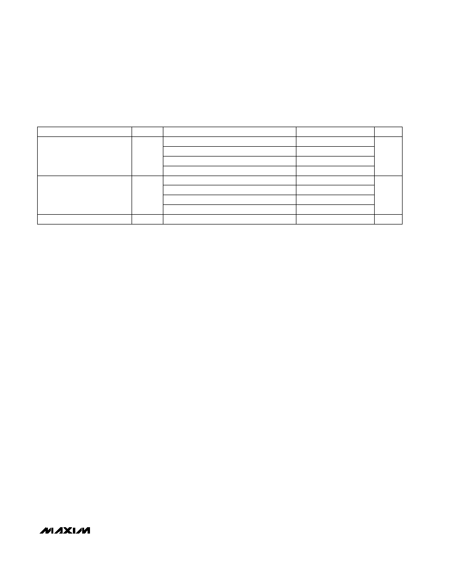
ABSOLUTE MAXIMUM RATINGS
ELECTRICAL CHARACTERISTICS
(AV
DD
= +5V ±5%, AV
SS
= -5V ±5%, DV
DD
= +5V ±5%, V
REFIN
= +2.5V (external reference), AGND = DGND = 0, 4.7µF capacitor
from REFOUT to AGND, 0.1µF capacitor from REFIN to AGND, f
CLK
= 16MHz, external clock, 50% duty cycle. T
A
= T
MIN
to T
MAX
,
unless otherwise noted. Typical values are at T
A
= +25°C.)
Stresses beyond those listed under "Absolute Maximum Ratings" may cause permanent damage to the device. These are stress ratings only, and functional
operation of the device at these or any other conditions beyond those indicated in the operational sections of the specifications is not implied. Exposure to
absolute maximum rating conditions for extended periods may affect device reliability.
AV
DD
to AGND ...........................................................-0.3V to 6V
AV
SS
to AGND ............................................................0.3V to -6V
DV
DD
to DGND ...........................................................-0.3V to 6V
AGND to DGND .......................................................-0.3V to 0.3V
CH_ _ to AGND....................................................................±17V
REFIN, REFOUT to AGND ..........................................-0.3V to 6V
Digital Inputs/Outputs to DGND ..............-0.3V to (DV
DD
+ 0.3V)
Continuous Power Dissipation (T
A
= +70°C)
36-Pin SSOP (derate 11.8mW/°C above +70°C) ..........941mW
Operating Temperature Ranges
MAX115_CAX/MAX116_CAX ...............................0°C to +70°C
MAX115_EAX/MAX116_EAX ............................-40°C to +85°C
Junction Temperature ......................................................+150°C
Storage Temperature Range .............................-65°C to +150°C
Lead Temperature (soldering, 10s)....................................300°C
CONDITIONS
UNITS
MIN
TYP
MAX
SYMBOL
PARAMETER
All channels
12
N
Resolution
Bits
0.6
±1
INL
Integral Nonlinearity (Note 2)
LSB
MAX115
±5
±15
Bipolar Zero Error
±30
Bipolar Zero-Error Match
Between all channels
mV
2
5
MAX115
180
µV/°C
Zero-Code Tempco
±5
±15
mV
Gain Error
±25
MAX115
2
5
mV
Gain Error Match
120
MAX115
Gain Error Tempco
µV/°C
SNR
Signal-to-Noise Ratio
dB
-80
THD
(Notes 4, 5)
Total Harmonic Distortion
dB
80
SFDR
(Note 4)
Spurious-Free Dynamic Range
dB
80
(Note 6)
Channel-to-Channel Isolation
dB
LSB
0.6
±1
DNL
Differential Nonlinearity
69
(Note 4)
MAX116
mV
±5
±10
±18
T
A
= +25°C
T
A
= T
MIN
to T
MAX
T
A
= +25°C
T
A
= T
MIN
to T
MAX
MAX116
90
±5
±10
±18
MAX116
T
A
= +25°C
T
A
= T
MIN
to T
MAX
T
A
= +25°C
T
A
= T
MIN
to T
MAX
60
MAX116
DC ACCURACY (Note 1)
DYNAMIC PERFORMANCE (f
CLK
= 16MHz, f
IN
= 10.06kHz) (Notes 1, 3)
MAX115/MAX116
2x4-Channel, Simultaneous-Sampling
12-Bit ADCs
_______________________________________________________________________________________
3
ELECTRICAL CHARACTERISTICS (continued)
(AV
DD
= +5V ±5%, AV
SS
= -5V ±5%, DV
DD
= +5V ±5%, V
REFIN
= +2.5V (external reference), AGND = DGND = 0, 4.7µF capacitor
from REFOUT to AGND, 0.1µF capacitor from REFIN to AGND, f
CLK
= 16MHz, external clock, 50% duty cycle. T
A
= T
MIN
to T
MAX
,
unless otherwise noted. Typical values are at T
A
= +25°C.)
CONDITIONS
UNITS
MIN
TYP
MAX
SYMBOL
PARAMETER
MAX115
V
±5
V
IN
Input Voltage Range
MAX115 (-5V to +5V range)
µA
±625
I
IN
Input Current
pF
16
C
IN
Input Capacitance
ns
600
t
ACQ
Acquisition Time
MHz
10
Small-Signal Bandwidth
MHz
1.3
Full-Power Bandwidth
mV/ms
2
Drop Rate
ns
10
Aperture Delay
ps
30
Aperture Jitter
ps
500
Aperture-Delay Matching
T
A
= +25°C
V
2.462
2.5
2.532
V
REFOUT
Output Voltage
0 < I
REF
< 1mA
mV/mA
0.5
External Load Regulation
(Note 8)
ppm/°C
30
REFOUT Tempco
µF
0.1
External Capacitive Bypass
at REFIN
V
2.40
2.50
2.60
Input Voltage Range
µF
4.7
22
External Capacitive Bypass
at REFOUT
µA
±50
Input Current
k
10
Input Resistance (Note 9)
pF
10
Input Capacitance
MHz
16
External Clock Frequency
V
2.4
V
IH
Input High Voltage
V
0.8
V
IL
Input Low Voltage
CONVST, RD, WR, CS, CLK
±1
pF
15
C
IN
Input Capacitance
A0A3
µA
±10
I
IN
Input Current
MAX116
±2.5
MAX116 (-2.5V to +2.5V range)
±15
MHz
5.6
10
14.8
Internal Clock Frequency
ANALOG INPUT
TRACK/HOLD
REFERENCE OUTPUT (Note 7)
REFERENCE INPUT
EXTERNAL CLOCK
DIGITAL INPUTS (CONVST, RD, WR, CS, CLK, A0A3) (Note 1)
INTERNAL CLOCK
MAX115/MAX116
2x4-Channel, Simultaneous-Sampling
12-Bit ADCs
4
_______________________________________________________________________________________
CONDITIONS
UNITS
MIN
TYP
MAX
SYMBOL
PARAMETER
I
OUT
= 1mA
V
4
V
OH
Output High Voltage
I
OUT
= -1.6mA
V
0.4
V
OL
Output Low Voltage
D0D11
µA
±10
Three-State Leakage Current
pF
10
Three-State Output
Capacitance
V
4.75
5
5.25
AV
DD
Positive Supply Voltage
V
-5.25
-5
-4.75
AV
SS
Negative Supply Voltage
V
4.75
5
5.25
DV
DD
Digital Supply Voltage
mA
17
25
I
AVDD
Positive Supply Current
mA
-20
-15
I
AVSS
Negative Supply Current
mA
3
6
Digital Supply Current
µA
1
Shutdown Positive Current
µA
-1
Shutdown Negative Current
µA
13
Shutdown Digital Current
(Note 10)
LSB
±1
PSRR+
Positive Supply Rejection
(Note 10)
LSB
±1
PSRR-
Negative Supply Rejection
(Note 11)
mW
175
Power Dissipation
DIGITAL OUTPUTS (D0D11, INT)
POWER REQUIREMENTS
ELECTRICAL CHARACTERISTICS (continued)
(AV
DD
= +5V ±5%, AV
SS
= -5V ±5%, DV
DD
= +5V ±5%, V
REFIN
= +2.5V (external reference), AGND = DGND = 0, 4.7µF capacitor
from REFOUT to AGND, 0.1µF capacitor from REFIN to AGND, f
CLK
= 16MHz, external clock, 50% duty cycle. T
A
= T
MIN
to T
MAX
,
unless otherwise noted. Typical values are at T
A
= +25°C.)
TIMING CHARACTERISTICS
(See Figure 4, AV
DD
= +5V, AV
SS
= -5V, DV
DD
= +5V, AGND = DGND = 0, T
A
= T
MIN
to T
MAX
, Typical values are at T
A
= +25°C,
unless otherwise noted.)
Guaranteed by design
ns
0
t
CWS
CS to WR Setup Time
Guaranteed by design
ns
0
t
CWH
CS to WR Hold Time
ns
30
t
WR
WR Low Pulse Width
ns
30
CONDITIONS
t
AS
Address Setup Time
ns
0
t
AH
Address Hold Time
25pF load
ns
55
t
ID
RD to INT Delay
ns
45
t
RD
Delay Time Between Reads
Guaranteed by design
ns
0
t
CRS
CS to RD Setup Time
Guaranteed by design
ns
0
t
CRH
CS to RD Hold Time
ns
30
t
RD
RD Low Pulse Width
25pF load (Note 12)
ns
40
t
DA
Data-Access Time
25pF load (Note 13)
ns
5
45
t
DH
Bus-Relinquish Time
ns
30
t
CW
CONVST Pulse Width
UNITS
MIN
TYP
MAX
SYMBOL
PARAMETER
MAX115/MAX116
2x4-Channel, Simultaneous-Sampling
12-Bit ADCs
_______________________________________________________________________________________
5
CONDITIONS
UNITS
MIN
TYP
MAX
SYMBOL
PARAMETER
TIMING CHARACTERISTICS (continued)
(See Figure 4, AV
DD
= +5V, AV
SS
= -5V, DV
DD
= +5V, AGND = DGND = 0, T
A
= T
MIN
to T
MAX
, Typical values are at T
A
= +25°C,
unless otherwise noted.)
Mode 1,
C
hannel 1
µs
2
Mode 2,
C
hannel 2
4
Mode 3,
C
hannel 3
6
Mode 4,
C
hannel 4
8
t
CONV
Exiting shutdown
ms
20
Startup Time
Note 1:
AV
DD
= +5V, AV
SS
= -5V, DV
DD
= +5V, V
REFIN
= 2.500V (external), V
IN
= ±5V (MAX115) or ±2.5V (MAX116).
Note 2:
Integral nonlinearity is the analog value's deviation at any code from its theoretical value after the full-scale range and
offset have been calibrated.
Note 3:
CLK synchronized with CONVST.
Note 4:
f
IN
= 10.06kHz, V
IN
= ±5V (MAX115) or ±2.5V (MAX116).
Note 5:
First five harmonics.
Note 6:
All inputs except CH1A driven with ±5V (MAX115) or ±2.5V (MAX116) 10.06kHz signal, CH1A connected to AGND and digi-
tized.
Note 7:
AV
DD
= DV
DD
= +5V, AV
SS
= -5V, V
IN
= 0V (all channels).
Note 8:
Temperature drift is defined as the change in output voltage from +25°C to T
MIN
or T
MAX
. It is calculated as
TC = [
REFOUT/REFOUT] / T.
Note 9:
See Figure 2.
Note 10: Defined as the change in positive full scale caused by a ±5% variation in the nominal supply voltage. Tested with one input
at full scale and all others at AGND. V
REFIN
= +2.5V (internal).
Note 11: Tested with all inputs connected to AGND. V
REFIN
= +2.5V (internal).
Note 12: The data access time is defined as the time required for an output to cross +0.8V or +2.0V. It is measured using the circuit
of Figure 1. The measured number is then extrapolated back to determine the value with a 25pF load.
Note 13: The bus relinquish time is derived from the measured time taken for the data outputs to change +0.5V when loaded with the
circuit of Figure 1. The measured number is then extrapolated back to remove the effects of charging and discharging the
120pF capacitor. The time given is the part's true bus relinquish time, which is independent of the external bus loading capac-
itance.
Conversion Time
Mode 1,
C
hannel 1
ksps
390
Conversion Rate
Mode 2,
C
hannel 2
218
Mode 3,
C
hannel 3
152
Mode 4,
C
hannel 4
116