
For price, delivery, and to place orders, please contact Maxim Distribution at 1-888-629-4642,
or visit Maxim's website at www.maxim-ic.com.
General Description
The MAX1102/MAX1103/MAX1104 CODECs provide
both an 8-bit analog-to-digital converter (ADC) and an
8-bit digital-to-analog converter (DAC) with a 4-wire
logic interface. The MAX1102/MAX1103 include an
onboard +2V/+4V reference, providing a well-regulat-
ed, low noise reference for both the ADC and DAC.
The MAX1104 offers ratiometric conversion, with the
reference internally connected to V
DD
.
The MAX1102/MAX1103/MAX1104 are low-cost, low-
power CODECs for use with microcontrollers (µCs).
They allow for greater flexibility when selecting a µC.
Less expensive µCs without onboard converters can be
used while maintaining overall system performance.
The MAX1102 operates from a single +2.7V to +3.6V
supply, the MAX1103 operates from a +4.5V to +5.5V
supply, and the MAX1104 operates from a +2.7V to
+5.5V supply. The MAX1102/MAX1103 incorporate a
V
DD
monitor in addition to AIN for power supply moni-
toring. All devices feature a low 18µA standby mode,
where both data converters are disabled while the ref-
erence remains active, and three shutdown modes:
ADC disabled, DAC disabled, and complete shutdown
(1µA). A quick 10µs wake-up time allows the
MAX1102/MAX1103/MAX1104 to cycle in and out of
shutdown even during short-duration idle times.
The MAX1102/MAX1103/MAX1104 are available in a
space-saving 8-pin µMAX package.
________________________Applications
Analog I/O for Microcontrollers
Analog System Signal Supervision
Voice Recording and Playback
Features
o 8-Bit ADC
±1LSB INL
Built-In Track-and-Hold
48dB of SINAD
o 8-Bit DAC
±1LSB INL
55dB of SFDR
o Internal Conversion Clock
o Single-Supply Operation
+2.7V to +3.6V (MAX1102)
+4.5V to +5.5V (MAX1103)
+2.7V to +5.5V (MAX1104)
o Low Power Consumption
0.5mA at 25ksps
1µA Shutdown Mode
o 6MHz 4-Wire SPITM, QSPITM, and MICROWIRETM
Compatible Interface
o Compact 8-Pin µMAX Package
o Internal Voltage Reference
+2V: MAX1102
+4V: MAX1103
o Power-Supply Monitor (MAX1102/MAX1103)
o Rail-to-Rail
®
DAC Output Buffer
MAX1102/MAX1103/MAX1104
8-Bit CODECs
________________________________________________________________ Maxim Integrated Products
1
1
2
3
4
8
7
6
5
DIN
DOUT
SCLK
CS
OUT
AIN
GND
V
DD
MAX1102
MAX1103
MAX1104
µMAX
TOP VIEW
Pin Configuration
SCLK
SERIAL
INTERFACE
AND
CONTROL
LOGIC
ADC
DAC
LATCH
T/H
AIN
V
DD/2
AOUT
VOLTAGE
REFERENCE
DIN
DOUT
MAX1102
MAX1103
MAX1104
GND
V
DD
DAC
CS
Functional Diagram
19-1873; Rev 0; 12/00
Ordering Information
PART
TEMP.
RANGE
PIN-
PACKAGE
REFER ENC E
MAX1102EUA
- 40
°C to + 85°C 8
µMAX
+2V
MAX1103EUA
- 40
°C to + 85°C 8
µMAX
+4V
MAX1104EUA
- 40
°C to + 85°C 8
µMAX
V
DD
SPI/QSPI are trademarks of Motorola, Inc.
MICROWIRE is a trademark of National Semiconductor Corp.
Rail-to-Rail is a registered trademark of Nippon Motorola Ltd.
MAX1102/MAX1103/MAX1104
8-Bit CODECs
2
_______________________________________________________________________________________
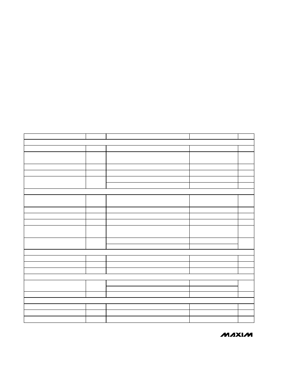
ABSOLUTE MAXIMUM RATINGS
ELECTRICAL CHARACTERISTICS
(V
DD
= +2.7V to +3.6V (MAX1102), V
DD
= +4.5V to +5.5V (MAX1103), V
DD
= +2.7V to +5.5V (MAX1104), f
SCLK
= 6.0MHz (50% duty
cycle), R
OUT
= 10k
, C
OUT
= 100pF, T
A
= T
MIN
to T
MAX
. Typical values are at T
A
= +25°C, unless otherwise noted.)
Stresses beyond those listed under "Absolute Maximum Ratings" may cause permanent damage to the device. These are stress ratings only, and functional
operation of the device at these or any other conditions beyond those indicated in the operational sections of the specifications is not implied. Exposure to
absolute maximum rating conditions for extended periods may affect device reliability.
V
DD
to GND ..............................................................-0.3V to +6V
AIN, OUT, DOUT to GND ...........................-0.3V to (V
DD
+ 0.3V)
DIN, SCLK, CS to GND ............................................-0.3V to +6V
Continuous Power Dissipation (T
A
= +70°C)
8-Pin µMAX (derate 4.1mW/°C above +70°C) .................330mW
Operating Temperature Range ...........................-40°C to +85°C
Maximum Junction Temperature .....................................+150°C
Storage Temperature Range .............................-65°C to +150°C
Lead Temperature (soldering,10s) ..................................+300°C
PARAMETER
SYM B O L CONDITIONS
MIN
TYP
MAX
UNITS
ADC DC ACCURACY (Note 1)
Resolution
8
Bits
Relative Accuracy
(Note 2)
INL
All codes
±1/4
±1
LSB
Differential Nonlinearity
DNL
Guaranteed monotonic
±1/4
±1
LSB
Offset Error
±1
LSB
MAX1102/MAX1103
±5
%
Gain Error
(Note 3)
MAX1104
±1
LSB
ADC DYNAMIC SPECIFICATIONS (f
AIN
= 10kHz SINE WAVE. V
AIN
= 0.9
V
REFp-p
)
Signal to Noise and Distortion
Ratio
SINAD
48
dB
Spurious-Free Dynamic Range
SFDR
59
dB
Total Harmonic Distortion
THD
58
dB
Full-Power Bandwidth
2.5
MHz
ADC Wake-Up Time from
Standby
Reference enabled (MAX1102/MAX1103)
3
µs
MAX1102/MAX11103
200
ADC Wake-Up Time from Full
Shutdown
MAX1104
3
µs
ANALOG INPUT
Analog Input Voltage
V
AIN
0
V
REF
V
Input Resistance
R
IN
10
M
Input Capacitance
C
IN
20
pF
VOLTAGE REFERENCE
MAX1102
2
Reference Voltage
V
REF
MAX1103
4
V
Temperature Coefficient
MAX1102/MAX1103
100
ppm/
o
C
CONVERSION RATE
Conversion Time
t
CONV
24
36
µs
Track/Hold Acquisition Time
t
ACQ
3.5
µs
Internal Clock Frequency
375
kHz

MAX1102/MAX1103/MAX1104
8-Bit CODECs
_______________________________________________________________________________________
3
PARAMETER
SYM B O L CONDITIONS
MIN
TYP
MAX
UNITS
Throughput Rate
ADC in continuous conversion mode
25
ksps
DAC DC ACCURACY
Resolution
8
Bits
Relative Accuracy
(Note 2)
INL
±1/4
±1
LSB
Differential Nonlinearity
DNL
Guaranteed monotonic
±1/4
±1
LSB
Offset Error
±30
mV
MAX1102/MAX1103
±5
%
Gain Error
(Note 3)
MAX1104
±30
mV
DAC DYNAMIC SPECIFICATIONS (f
OUT
= 1kHz SINE WAVE, V
OUT
= 0.9
V
REFp-p
)
Spurious-Free Dynamic Range
SFDR
55
dB
Total Harmonic Distortion
THD
53
dB
Small-Signal Bandwidth
1
MHz
Full-Power Bandwidth
72
kHz
DAC Wake-Up Time from
Standby (Note 4)
Reference enabled (MAX1102/MAX1103)
10
µs
MAX1102/MAX1103
200
DAC Wake-Up Time from Full
Shutdown (Note 4)
MAX1104
10
µs
DAC OUTPUT
Full-Scale Swing
MAX1104
0
V
DD
-
0.1
V
Settling Time (Note 5)
Settle to within
±1/2 LSB
11
µs
Slew Rate
1.2
V/
µs
Load Regulation
R
L
open to 10k
0 < V
OUT
< V
DD
- 0.1V
0.05
LSB
LOGIC INPUTS AND OUTPUTS (DIN, SLCK, CS)
Input High Voltage
V
IH
V
DD
0.7
V
Input Low Voltage
V
IL
V
DD
0.3
V
Input Current
V
LOGIC
= GND or V
DD
±0.1
±5
µA
Digital Input Hysteresis
0.5
V
Digital Input Capacitance
15
pF
Output High Voltage
V
OH
I
SOURCE
= 1.0mA
V
DD
0.9
V
Output Low Voltage
V
OL
I
SINK
= 1.0mA
V
DD
0.1
V
Three-State Leakage
I
LEAK
±5.0
µA
ELECTRICAL CHARACTERISTICS (continued)
(V
DD
= +2.7V to +3.6V (MAX1102), V
DD
= +4.5V to +5.5V (MAX1103), V
DD
= +2.7V to +5.5V (MAX1104), f
SCLK
= 6.0MHz (50% duty
cycle), R
OUT
= 10k
, C
OUT
= 100pF, T
A
= T
MIN
to T
MAX
. Typical values are at T
A
= +25°C unless otherwise noted.)

MAX1102/MAX1103/MAX1104
8-Bit CODECs
4
_______________________________________________________________________________________
Note 1: MAX1102/MAX1104 tested with V
DD
= +3V. MAX1103 tested with V
DD
= +5V.
Note 2: Relative accuracy is the deviation of the analog value at any code from its theoretical value after the gain error and offset
error have been nulled.
Note 3: Gain error calculation is referenced to the ideal FS output. Gain error for the MAX1102/MAX1103 also includes reference ini-
tial accuracy error.
Note 4: Wake-up time is the time it takes for the DAC output to settle to within ±1/2 LSB of the FS value after a power-up command.
Note 5: Output settling time is measured by taking the DAC from code 00hex to FFhex.
PARAMETER
SYM B O L CONDITIONS
MIN
TYP
MAX
UNITS
POWER SUPPLY REQUIREMENTS
MAX1102
2.7
3.6
MAX1103
4.5
5.5
Supply Voltage
V
DD
MAX1104
2.7
5.5
V
ADC on (25ksps), DAC off
0.25
0.5
Supply Current
I
CC
ADC off, DAC on (V
DD
= +5.5V)
0.4
0.66
mA
Standby Current
ADC off, DAC off, clock off, reference on
18
35
µA
Full Shutdown Current
ADC off, DAC off, clock off
1
µA
ELECTRICAL CHARACTERISTICS (continued)
(V
DD
= +2.7V to +3.6V (MAX1102), V
DD
= +4.5V to +5.5V (MAX1103), V
DD
= +2.7V to +5.5V (MAX1104), f
SCLK
= 6.0MHz (50% duty
cycle), R
OUT
= 10k
, C
OUT
= 100pF, T
A
= T
MIN
to T
MAX
. Typical values are at T
A
= +25°C unless otherwise noted.)
PARAMETER
SYM B O L CONDITIONS
MIN
TYP
MAX
UNITS
Power Up to Reset Complete
t9
40
µs
CS Rise-to-DOUT = High-Z
t10
40
ns
CS Fall-to-DOUT Valid
t11
R
DOUT
= 3k
, C
DOUT
= 50pF
60
ns
CS Fall-to-SCLK Rise
t3
15
ns
SCLK Fall-to-CS Rise
t8
25
ns
DIN-to-SCLK Setup Time
t4
10
ns
DIN-to-SCLK Hold Time
t5
15
ns
SCLK Fall to DOUT Valid
t6
R
DOUT
= 3k
, C
DOUT
= 50pF
70
ns
SCLK Maximum Frequency
f
SCLK
6
MHz
SCLK Pulse Width High
t
CH
60
ns
SCLK Pulse Width Low
t
CL
70
ns
TIMING CHARACTERISTICS (Figures 4a and 4b)
(V
DD
= +2.7V to +3.6V (MAX1102), V
DD
= +4.5V to +5.5V (MAX1103), V
DD
= +2.7V to +5.5V (MAX1104), f
SCLK
= 6.0MHz (50% duty
cycle), R
OUT
= 10k
, C
OUT
= 100pF, T
A
= T
MIN
to T
MAX
. Typical values are at T
A
= +25°C unless otherwise noted.)

MAX1102/MAX1103/MAX1104
8-Bit CODECs
0
100
50
200
150
250
300
2.5
3.5
4.0
3.0
4.5
5.0
5.5
SUPPLY CURRENT vs. SUPPLY VOLTAGE
(ADC ENABLED, DAC DISABLED)
MAX1102 toc01
SUPPLY VOLTAGE (V)
SUPPLY CURRENT (
µ
A)
CODE = AAhex
0
150
50
250
200
300
350
2.5
3.5
4.0
3.0
4.5
5.0
5.5
SUPPLY CURRENT vs. SUPPLY VOLTAGE
(DAC ENABLED, ADC DISABLED)
MAX1102 toc02
SUPPLY VOLTAGE (V)
SUPPLY CURRENT (
µ
A)
CODE = FFhex
100
CODE = 00hex
0
400
350
450
500
2.5
3.5
4.0
3.0
4.5
5.0
5.5
SUPPLY CURRENT vs. SUPPLY VOLTAGE
(ADC ENABLED, DAC ENABLED)
MAX1102 toc03
SUPPLY VOLTAGE (V)
SUPPLY CURRENT (
µ
A)
DAC CODE = FFhex
200
150
250
300
50
100
DAC CODE = 00hex
ADC CODE = AAhex
20
15
10
5
0
2.5
4.0
3.0
3.5
4.5
5.0
5.5
SHUTDOWN SUPPLY CURRENT vs.
SUPPLY VOLTAGE
MAX1102 toc04
SUPPLY VOLTAGE (V)
SUPPLY CURRENT (
µ
A)
ADC and DAC OFF
REFERENCE ON
ADC, DAC, and
REFERENCE OFF
0
1.5
1.0
0.5
2.0
2.5
3.0
3.5
4.0
4.5
5.0
2.5
3.5
3.0
4.0
4.5
5.0
5.5
ADC OFFSET ERROR vs.
SUPPLY VOLTAGE
MAX1102 toc05
SUPPLY VOLTAGE (V)
OFFSET ERROR (mV)
5
6
8
7
9
10
2.5
3.5
3.0
4.0
4.5
5.0
5.5
DAC OFFSET ERROR
vs. SUPPLY VOLTAGE
MAX1102 toc06
SUPPLY VOLTAGE (V)
OFFSET ERROR (mV)
CODE = 0Ahex
0
0.25
0.50
0.75
1.00
1.25
1.50
1.75
2.00
2.5
3.5
3.0
4.0
4.5
5.0
5.5
ADC GAIN ERROR
vs. SUPPLY VOLTAGE
MAX1102 toc07
SUPPLY VOLTAGE (V)
GAIN ERROR (%FS)
V
REF
= 2.0V
CODE = FFhex
0
3
2
1
4
5
6
7
8
9
10
-40
10
-15
35
60
85
ADC GAIN ERROR vs. TEMPERATURE
MAX1102 toc08
TEMPERATURE (
°C)
GAIN ERROR (mV)
V
REF
= 2.0V
CODE = 7Fhex
0
3
2
1
4
5
6
7
8
9
10
2.5
3.5
3.0
4.0
4.5
5.0
DAC GAIN ERROR vs. SUPPLY VOLTAGE
MAX1102 toc09
SUPPLY VOLTAGE (V)
GAIN ERROR (mV)
5.5
V
REF
= 2.0V
CODE = FFhex
Typical Operating Characteristics
(V
DD
= +3.0V (MAX1102), V
DD
= +5V (MAX1103), f
SCLK
= 6.0MHz (50% duty cycle), R
OUT
= 10k
, C
OUT
= 100pF, T
A
= +25°C,
unless otherwise noted.)
_______________________________________________________________________________________
5