
1 of 12
110602
FEATURES
§ 10 years minimum data retention in the
absence of external power
§ Data is automatically protected during power
loss
§ Power supply monitor resets processor when
V
CC
power loss occurs and holds processor in
reset during V
CC
ramp-up
§ Battery monitor checks remaining capacity
daily
§ Read and write access times as fast as 70ns
§ Unlimited write cycle endurance
§ Typical standby current 50mA
§ Upgrade for 512k x 8 SRAM, EEPROM, or
Flash
§ Lithium battery is electrically disconnected to
retain freshness until power is applied for the
first time
§ Full ±10% V
CC
operating range (DS1350Y)
or optional
±5% V
CC
operating range
(DS1350AB)
§ Optional industrial temperature range of
-40
°C to +85°C, designated IND
§ PowerCap Module (PCM) package
- Directly surface-mountable module
- Replaceable snap-on PowerCap provides
lithium backup battery
- Standardized pinout for all nonvolatile
(NV) SRAM products
- Detachment feature on PowerCap allows
easy removal using a regular screwdriver
PIN ASSIGNMENT
PIN DESCRIPTION
A0 A18
- Address Inputs
DQ0 DQ7
- Data In/Data Out
CE
- Chip Enable
WE
- Write Enable
OE
- Output Enable
RST
- Reset Output
BW
- Battery Warning
V
CC
- Power (+5V)
GND -
Ground
DESCRIPTION
The DS1350 4096k NV SRAMs are 4,194,304 bit, fully static, NV SRAMs organized as 524,288 words
by 8 bits. Each NV SRAM has a self-contained lithium energy source and control circuitry, which
constantly monitors V
CC
for an out-of-tolerance condition. When such a condition occurs, the lithium
energy source is automatically switched on and write protection is unconditionally enabled to prevent
data corruption. Additionally, the DS1350 devices have dedicated circuitry for monitoring the status of
V
CC
and the status of the internal lithium battery. DS1350 devices in the PowerCap Module package are
directly surface mountable and are normally paired with a DS9034PC PowerCap to form a complete NV
SRAM module. The devices can be used in place of 512k x 8 SRAM, EEPROM or Flash components.
DS1350Y/AB
4096k Nonvolatile SRAM
with Battery Monitor
www.maxim-ic.com
1
BW
2
3
A15
A16
RST
V
CC
WE
OE
CE
DQ7
DQ6
DQ5
DQ4
DQ3
DQ2
DQ1
DQ0
GND
4
5
6
7
8
9
10
11
12
13
14
15
16
17
A17
A14
33
32
31
30
29
28
27
26
25
24
23
22
21
20
19
18
A13
A12
A11
A10
A9
A8
A7
A6
A5
A4
A3
A2
A1
A0
34
A18
GND V
BAT
34-Pin PowerCap Module (PCM)
(Uses DS9034PC PowerCap)

DS1350Y/AB
2 of 12
READ MODE
The DS1350 devices execute a read cycle whenever
WE
(Write Enable) is inactive (high) and
CE
(Chip
Enable) and
OE
(Output Enable) are active (low). The unique address specified by the 19 address inputs
(A
0
-A
18
) defines which of the 524,288 bytes of data is to be accessed. Valid data will be available to the
eight data output drivers within t
ACC
(Access Time) after the last address input signal is stable, providing
that
CE
and
OE
(Output Enable) access times are also satisfied. If
OE
and
CE
access times are not
satisfied, then data access must be measured from the later-occurring signal (
CE
or
OE
) and the limiting
parameter is either t
CO
for
CE
or t
OE
for
OE
rather than address access.
WRITE MODE
The DS1350 devices execute a write cycle whenever the
WE
and
CE
signals are in the active (low) state
after address inputs are stable. The later-occurring falling edge of
CE
or
WE
will determine the start of
the write cycle. The write cycle is terminated by the earlier rising edge of
CE
or
WE
. All address inputs
must be kept valid throughout the write cycle.
WE
must return to the high state for a minimum recovery
time (t
WR
) before another cycle can be initiated. The
OE
control signal should be kept inactive (high)
during write cycles to avoid bus contention. However, if the output drivers are enabled (
CE
and
OE
active) then
WE
will disable the outputs in t
ODW
from its falling edge.
DATA RETENTION MODE
The DS1350AB provides full functional capability for V
CC
greater than 4.75V and write protects by 4.5V.
The DS1350Y provides full functional capability for V
CC
greater than 4.5V and write protects by 4.25V.
Data is maintained in the absence of V
CC
without any additional support circuitry. The NV SRAMs
constantly monitor V
CC
. Should the supply voltage decay, the NV SRAMs automatically write protect
themselves, all inputs become "don't care," and all outputs become high-impedance. As V
CC
falls below
approximately 2.7V, the power switching circuit connects the lithium energy source to RAM to retain
data. During power-up, when V
CC
rises above approximately 2.7V, the power switching circuit connects
external V
CC
to the RAM and disconnects the lithium energy source. Normal RAM operation can resume
after V
CC
exceeds 4.75V for the DS1350AB and 4.5V for the DS1350Y.
SYSTEM POWER MONITORING
DS1350 devices have the ability to monitor the external V
CC
power supply. When an out-of-tolerance
power supply condition is detected, the NV SRAMs warn a processor-based system of impending power
failure by asserting
RST
. On power-up,
RST
is held active for 200ms nominal to prevent system
operation during power-on transients and to allow t
REC
to elapse.
RST
has an open drain output driver.
BATTERY MONITORING
The DS1350 devices automatically perform periodic battery voltage monitoring on a 24-hour time
interval. Such monitoring begins within t
REC
after V
CC
rises above V
TP
and is suspended when power
failure occurs.
After each 24-hour period has elapsed, the battery is connected to an internal 1M
W test resistor for one
second. During this one second, if battery voltage falls below the battery voltage trip point (2.6V), the
battery warning output
BW
is asserted. Once asserted,
BW
remains active until the module is replaced.
The battery is still retested after each V
CC
power-up, however, even if
BW
is active. If the battery voltage
is found to be higher than 2.6V during such testing,
BW
is de-asserted and regular 24-hour testing
resumes.
BW
has an open drain output driver.
DS1350Y/AB
4 of 12
ABSOLUTE MAXIMUM RATINGS*
Voltage on Any Pin Relative to Ground
-0.3V to +7.0V
Operating Temperature Range
0°C to 70°C, -40°C to +85°C for IND parts
Storage Temperature Range
-40°C to +70°C, -40°C to +85°C for IND parts
Soldering Temperature
260°C for 10 seconds
* This is a stress rating only and functional operation of the device at these or any other conditions
above those indicated in the operation sections of this specification is not implied. Exposure to
absolute maximum rating conditions for extended periods of time may affect reliability.
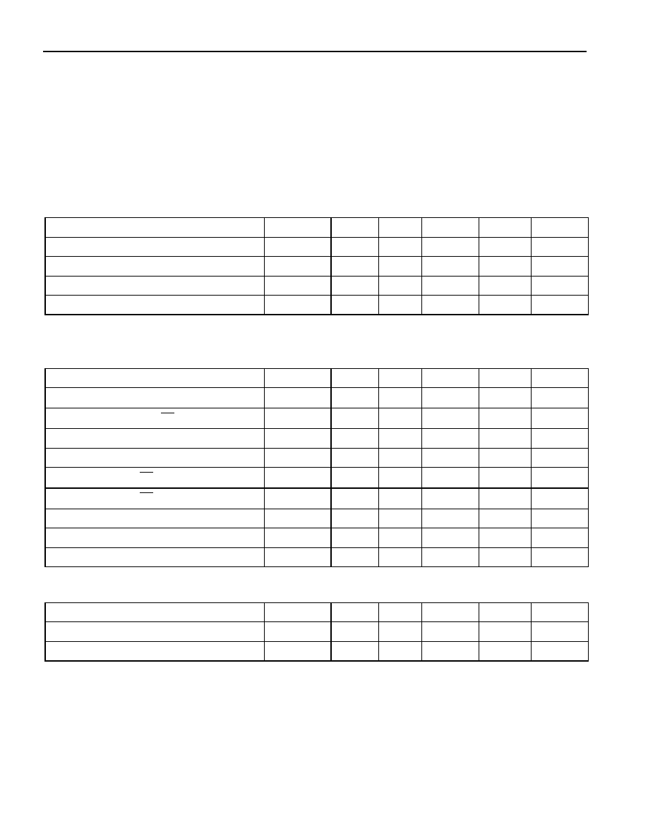
RECOMMENDED DC OPERATING CONDITIONS
(t
A
: See Note 10)
PARAMETER
SYMBOL
MIN
TYP
MAX
UNITS NOTES
DS1350AB Power Supply Voltage
V
CC
4.75
5.0
5.25
V
DS1350Y Power Supply Voltage
V
CC
4.5
5.0
5.5
V
Logic 1
V
IH
2.2
V
CC
V
Logic 0
V
IL
0.0
0.8
V
DC ELECTRICAL (V
CC
= 5V
± 5% for DS1350AB)
CHARACTERISTICS (t
A
: See Note 10) (V
CC
= 5V
± 10% for DS1350Y)
PARAMETER
SYMBOL
MIN
TYP
MAX
UNITS NOTES
Input Leakage Current
I
IL
-1.0
+1.0
mA
I/O Leakage Current
CE
ł V
IH
Ł V
CC
I
IO
-1.0
+1.0
mA
Output Current @ 2.4V
I
OH
-1.0
mA
14
Output Current @ 0.4V
I
OL
2.0
mA
14
Standby Current
CE
=2.2V
I
CCS1
200
600
mA
Standby Current
CE
=V
CC
-0.5V
I
CCS2
50
150
mA
Operating Current
I
CCO1
85
mA
Write Protection Voltage (DS1350AB)
V
TP
4.50
4.62
4.75
V
Write Protection Voltage (DS1350Y)
V
TP
4.25
4.37
4.5
V
CAPACITANCE
(
t
A
= 25
°
C)
PARAMETER
SYMBOL
MIN
TYP
MAX
UNITS NOTES
Input Capacitance
C
IN
5
10
pF
Input/Output Capacitance
C
I/O
5
10
pF

