1 of 16
101001
FEATURES
§ Step sizes of 0.25 ns, 0.5 ns, 1 ns, 2 ns, 5 ns
§ On-chip reference delay
§ Configurable as delay line, pulse width
modulator, or free-running oscillator
§ Can delay clocks by a full period or more
§ Guaranteed monotonicity
§ Parallel or serial programming
§ Single 5V supply
§ 16-pin DIP or SOIC package
PIN ASSIGNMENT
PIN DESCRIPTION
IN -
Input
P0/Q -
Parallel
Input
P0 (parallel mode)
- Serial Data Output (serial mode)
P1/CLK -
Parallel
Input P1 (parallel mode)
- Serial Input Clock (serial mode)
P2/D -
Parallel
Input
P2 (parallel mode)
- Serial Data Input (serial mode)
P3 - P7
- Remaining Parallel Inputs
GND -
Ground
OUT/
OUT
-
Output
REF/PWM
- Reference or PWM Output
P
/S
- Parallel / Serial Programming
Select
MS
- Output Mode Select
LE
- Input Latch Enable
V
CC
- Supply Voltage
DESCRIPTION
The DS1023 is an 8-bit programmable delay line similar in function to the DS1020/DS1021.
Additional features have been added to extend the range of applications:
The internal delay line architecture has been revised to allow clock signals to be delayed by up to a full
period or more. Combined with an on-chip reference delay (to offset the inherent or "step zero" delay of
the device) clock phase can now be varied over the full 0-360 degree range.
DS1023
8-Bit Programmable Timing Element
www.maxim-ic.com
IN
LE
Q/P0
CLK/P1
D/P2
P3
P4
GND
16
15
14
13
12
11
10
9
V
CC
OUT/OUT
REF/PWM
P/S
P7
P6
MS
P5
1
2
3
4
5
6
7
8
DS1023 300-mil DIP
DS1023S 300-mil SOIC

DS1023
2 of 16
On-chip gating is provided to allow the device to provide a pulse width modulated output, triggered by
the input with duration set by the programmed value.
Alternatively the output signal may be inverted on chip, allowing the device to perform as a free-running
oscillator if the output is (externally) connected to the input.
PROGRAMMING
The device programming is identical to the DS1020/DS1021. Note, however, that the serial clock and
data pins are shared with three of the parallel input pins.
The
P
/S pin controls the same function as "Mode Select" on the DS1020/DS1021 (but with reversed
polarity). A low logic level on this pin enables the parallel programming mode. LE must be at a high
logic level to alter the programmed value; when LE is taken low the data is latched internally and the
parallel data inputs may be altered without affecting the programmed value. This is useful for
multiplexed bus applications. For hard-wired applications LE should be tied to a high logic level.
When
P
/S is high serial programming is enabled. LE must be held high to enable loading or reading of
the internal register, during which time the delay is determined by the previously programmed value.
Data is clocked in MSB to LSB order on the rising edge of the CLK input. Data transfer ends and the
new value is activated when LE is taken low.
PARALLEL MODE (
P
/S = 0)
In the PARALLEL programming mode, the output of the DS1023 will reproduce the logic state of the
input after a delay determined by the state of the eight program input pins P0 - P7. The parallel inputs
can be programmed using DC levels or computer-generated data. For infrequent modification of the
delay value, jumpers may be used to connect the input pins to V
CC
or ground. For applications requiring
frequent timing adjustment, DIP switches may be used. The latch enable pin (LE) must be at a logic 1 in
hardwired implementations.
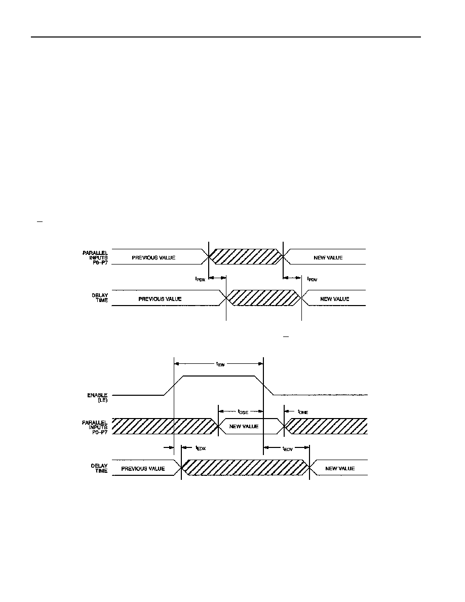
Maximum flexibility is obtained when the eight parallel programming bits are set using computer-
generated data. When the data setup (t
DSE
) and data hold (t
DHE
) requirements are observed, the enable pin
can be used to latch data supplied on an 8-bit bus. Latch enable must be held at a logic 1 if it is not used
to latch the data. After each change in delay value, a settling time (t
EDV
or t
PDV
) is required before input
logic levels are accurately delayed.
SERIAL MODE (
P
/S = 1)
In the SERIAL programming mode, the output of the DS1023 will reproduce the logic state of the input
after a delay time determined by an 8-bit value clocked into serial port D. While observing data setup
(t
DSC
) and data hold (t
DHC
) requirements, timing data is loaded in MSB-to-LSB order by the rising edge of
the serial clock (CLK). The latch enable pin (LE) must be at a logic 1 to load or read the internal 8-bit
input register, during which time the delay is determined by the last value activated. Data transfer ends
and the new delay value is activated when latch enable (LE) returns to a logic 0. After each change, a
settling time (t
EDV
) is required before the delay is accurate.
As timing values are shifted into the serial data input (D), the previous contents of the 8-bit input register
are shifted out of the serial output pin (Q) in MSB-to-LSB order. By connecting the serial output of one
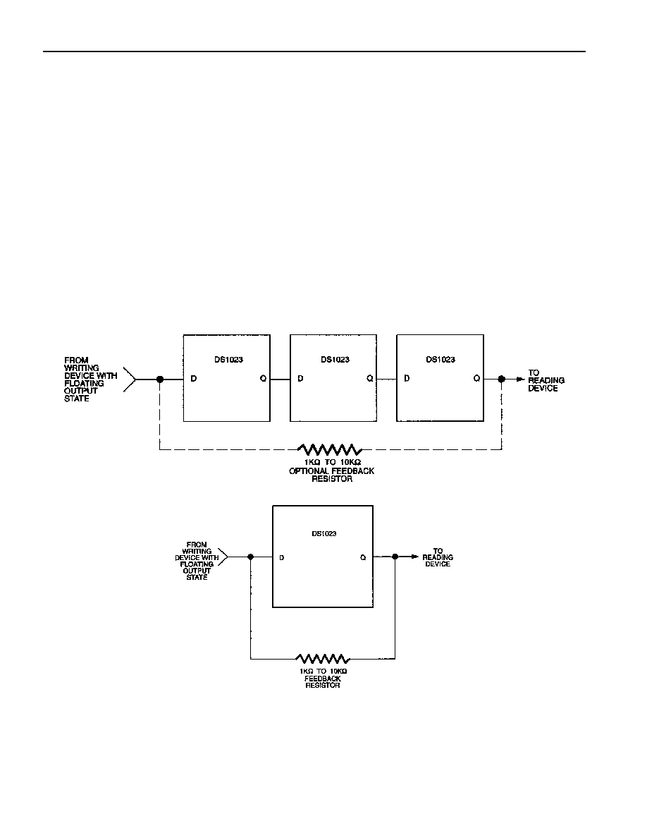
DS1023 to the serial input of a second DS1023, multiple devices can be daisy-chained (cascaded) for
programming purposes (Figure 1). The total number of serial bits must be eight times the number of units
daisy-chained and each group of 8 bits must be sent in MSB-to-LSB order.
DS1023
3 of 16
Applications can read the setting of the DS1023 Delay Line by connecting the serial output pin (Q) to the
serial input (D) through a resistor with a value of 1 to 10 kohms (Figure 2). Since the read process is
destructive, the resistor restores the value read and provides isolation when writing to the device. The
resistor must connect the serial output (Q) of the last device to the serial input (D) of the first device of a
daisy chain (Figure 1). For serial readout with automatic restoration through a resistor, the device used to
write serial data must go to a high impedance state.
To initiate a serial read, latch enable (LE) is taken to a logic 1 while serial clock (CLK) is at a logic 0.
After a waiting time (t
EQV
), bit 7 (MSB) appears on the serial output (Q). On the first rising (0 --> 1)
transition of the serial clock (CLK), bit 7 (MSB) is rewritten and bit 6 appears on the output after a time
t
CQV
. To restore the input register to its original state, this clocking process must be repeated eight times.
In the case of a daisy chain, the process must be repeated eight times per package. If the value read is
restored before latch enable (LE) is returned to logic 0, no settling time (t
EDV
) is required and the
programmed delay remains unchanged.
Since the DS1023 is a CMOS design, unused input pins (P3 - P7) must be connected to well-defined logic
levels; they must not be allowed to float. Serial output Q/P0 should be allowed to float if unused.
CASCADING MULTIPLE DEVICES (DAISY CHAIN) Figure 1
SERIAL READOUT
Figure 2
REFERENCE DELAY
In all delay lines there is an inherent, or "step zero", delay caused by the propagation delay through the
input and output buffers. In this device the step zero delay can be quite large compared to the delay step
size. To simplify system design a reference delay has been included on chip which may be used to
compensate for the step zero delay. In practice this means that if the device is supplied with a clock, for
example, the minimum programmed output delay is effectively zero with respect to the reference delay.

DS1023
4 of 16
For highest accuracy it is strongly recommended that the reference delay is used. Variations in input
voltage levels and transition times can significantly alter the measured delay from input to output. This
effect is totally removed if the reference delay output is used. Furthermore, adverse effects on step zero
delay caused by process temperature coefficients are also cancelled out.
INPUT PULSE DURATION
The internal architecture of the DS1023 allows the output delay time to be considerably longer than the
input pulse width (see ac specifications). This feature is useful in many applications, in particular clock
phase control where delays up to and beyond one full clock period can be achieved.
MODE SELECT
The DS1023 has four possible output functions but only two output pins. The functionality of the two
output pins is determined by the Mode Select (MS) pin.
MS = 0
Figure 3
Output Function
Name
Pin Number
Reference Output
REF
9
Delayed Output
OUT
15
OUT is a copy of the input waveform that is delayed by an amount set by the programmed values (Table
1). A programmed value of zero will still result in a non-zero delay as indicated in the Step Zero delay
specification. The signal on OUT is the same polarity as the input.
REF is a fixed reference delay. It also is a copy of the input waveform but the delay interval is fixed to a
value approximately equal to the Step Zero Value of the device (as shown in the Reference Delay
specification). In fact the device is trimmed to ensure that the Reference Delay is always slightly longer
than the Step Zero Value (by 1.5 ns typically).
DS1023
5 of 16
MS = 1 Figure 4
Output Function
Name
Pin Number
Pulse Width Modulated Output
PWM
9
Delayed and Inverted Output
OUT
15
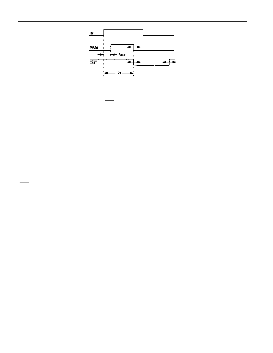
PWM is an output triggered by the rising edge of the input waveform. After a time interval approximately
equal to the Step Zero delay of the device the PWM output will go high. The output will return to a low
level after a time interval determined by the programmed values (Table 1). Hence output pulse widths can
be obtained from (nearly) zero to the full delay range of the device. In practice the minimum output pulse
width is limited by the response time of the device to approximately 5ns. Programmed values less than
this will result in degradation of the output high level voltage until ultimately no discernible output pulse
is produced. The frequency/repetition rate of the output is determined by the input frequency. The input
pulse width can be shorter than the output pulse width, and is limited only by the minimum input pulse
width specification. The PWM function is not "re-triggerable", subsequent input trigger pulses should
not be present until the output has returned to a low level.
OUT
is an inverted copy of the input waveform that is delayed by an amount set by the programmed
values (Table 1). A programmed value of zero will still result in a non-zero delay as indicated in the Step
Zero delay specification. The
OUT
pin may also be externally connected to the input pin to produce a
free-running oscillator. The frequency of oscillation is determined by the programmed delay value of the
device (see Table 2).
DS1023
6 of 16
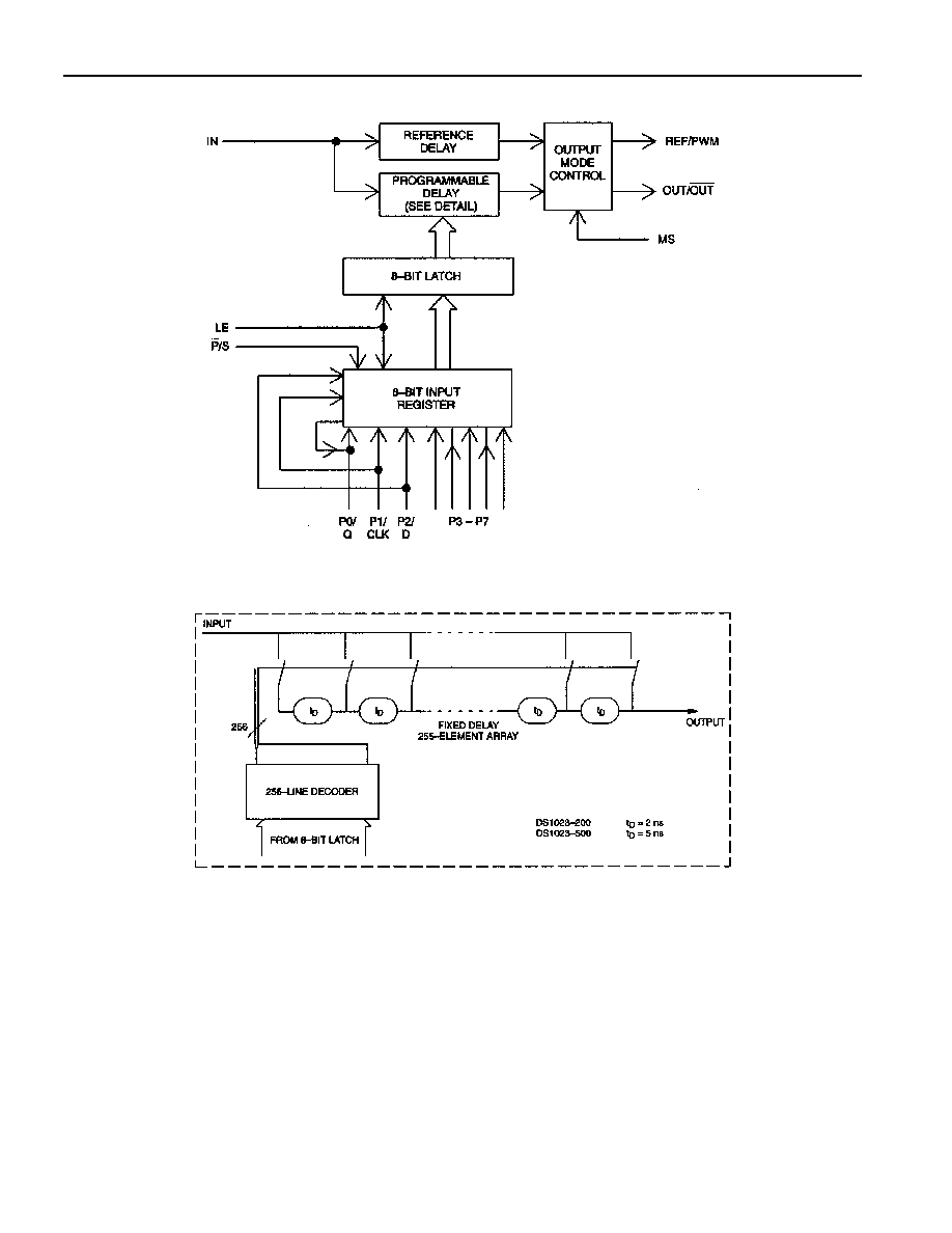
FUNCTIONAL BLOCK DIAGRAM
Figure 5
DELAY LINE DETAIL (CONCEPTUAL) - DS1023-200, DS1023-500
Figure 6
DS1023
7 of 16
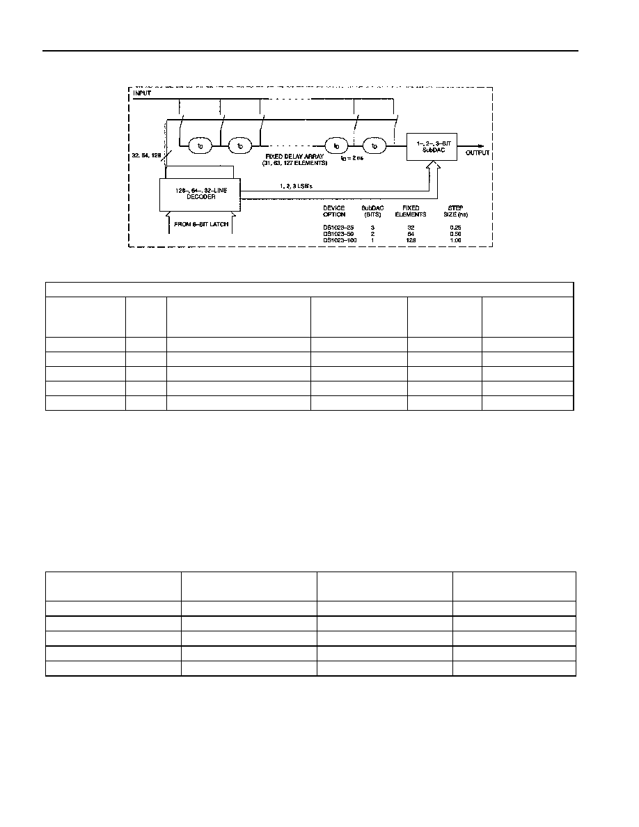
DELAY LINE DETAIL (CONCEPTUAL) - DS1023-25, DS1023-50, DS1023-100
Figure 7
PART NUMBER TABLE
Table 1
DELAYS RANGES AND TOLERANCE (all times measured in ns)
PART
NUMBER
STEP
SIZE
MAX. DELAY TIME (1)/
MAX. OUTPUT PULSE
WIDTH (2)
MAXIMUM
DEVIATION (3)
MAXIMUM
I/P FREQ
MINIMUM I/P
PULSE
WIDTH
DS1023-25
0.25
63.75
±1
25 MHz
20
DS1023-50
0.50
127.5
±2
25 MHz
20
DS1023-100
1.0
255
±4
25 MHz
20
DS1023-200
2.0
510
±8
25 MHz
20
DS1023-500
5.0
1275
±20
10 MHz
50
1. In "Normal" mode (MS=0). Measured with respect to REF output. The minimum delay time is zero
(or less, by 1.5 ns typically)
2. In PWM mode (MS=1). The minimum output pulse width for reliable operation is 5 ns; programmed
values less than this may produce reduced output voltage levels or no output at all.
3. This is the deviation from a straight line drawn between the step zero value and the maximum
programmed delay time.
OSCILLATOR CONFIGURATION
Table 2
PART NUMBER
STEP
SIZE (4)
MINIMUM O/P
FREQUENCY (5)
MAXIMUM O/P
FREQUENCY (5)
DS1023-25
0.5
6.6 MHz
22 MHz
DS1023-50
1.0
3.6 MHz
22 MHz
DS1023-100
2.0
1.9 MHz
22 MHz
DS1023-200
4.0
0.98 MHz
22 MHz
DS1023-500
10.0
0.4 MHz
22 MHz
4. Step size in output period (in ns).
5. Maximum output frequency depends on the actual step zero delay value, worst case values are shown
in the table. The output period is given by: 2 * t
D
where: t
D
= absolute delay value.

DS1023
8 of 16
DALLAS SEMICONDUCTOR TEST CIRCUIT
Figure 8
TEST SETUP DESCRIPTION
Figure 8 illustrates the hardware configuration used for measuring the timing parameters of the DS1023.
The input waveform is produced by a precision pulse generator under software control. Time delays are
measured by a time interval counter (20 ps resolution) connected to the output. The DS1023 serial and
parallel ports are controlled by interfaces to a central computer. All measurements are fully automated
with each instrument controlled by the computer over an IEEE 488 bus.
TEST CONDITIONS
INPUT:
Ambient Temperature:
25
°C ± 3°C
Supply Voltage (V
CC
):
5.0V
± 0.1V
Input Pulse:
High = 3.0V
± 0.1V
Low = 0.0V
± 0.1V
Source Impedance:
50 ohms max.
Rise and Fall Time:
3.0 ns max.
(measured between
0.6V and 2.4V)
Pulse Width:
500 ns
Period:
1
ms
NOTE: Above conditions are for test only and do not restrict the operation of the device under other data
sheet conditions.
OUTPUT:
Output is loaded with a 74F04. Delay is measured between the 1.5V level of the rising edge of the input
signal and the 1.5V level of the corresponding edge of the output.

DS1023
9 of 16
ABSOLUTE MAXIMUM RATINGS*
Voltage on Any Pin
-1.0V to +7.0V
Operating Temperature Range
0
°C to 70°C
Storage Temperature
-55
°C to +125°C
Soldering Temperature
260
°C for 10 seconds
Short Circuit Output Current
50 mA for 1 second
* This is a stress rating only and functional operation of the device at these or any other conditions above
those indicated in the operation sections of this specification is not implied. Exposure to absolute
maximum rating conditions for extended periods of time may affect reliability.
DC ELECTRICAL CHARACTERISTICS
(0°C to 70°C; V
CC
= 5V ± 5%)
PARAMETER
SYMBOL
MIN
TYP
MAX
UNITS
NOTES
Supply Voltage
V
CC
4.75
5
5.25
V
High Level Input Voltage
V
IH
2
V
CC
+0.5
V
Low Level Input Voltage
V
IL
-0.5
0.8
V
Input Leakage Current
(0<V
I
<V
CC
)
I
I
-1
+1
µA
Active Current
I
CC
30
60
mA
High Level Output Current
(V
CC
= Min, V
OH
= 2.7V)
I
OH
-1
mA
Low Level Output Current
(V
CC
= Min, V
OL
= 0.5V)
-Q output
-
All other outputs
I
OL
I
OL
4
8
mA
mA
AC ELECTRICAL CHARACTERISTICS - CONTROL/INTERFACE
SPECIFICATIONS ALL SPEED OPTIONS
(T
A
= 0
°C to 70°C; V
CC
= 5V
± 5%)
PARAMETER
SYMBOL
MIN
TYP
MAX
UNITS
NOTES
Serial Clock Frequency
f
CLK
10
MHz
Input Pulse Width (LE, CLK)
t
W
50
ns
Data Setup to Clock
t
DSC
30
ns
Data Hold from Clock
t
DHC
0
ns
Data Setup to Enable
t
DSE
30
ns
Data Hold from Enable
t
DHE
0
ns
Enable Setup to Clock
t
ES
0
ns
Enable Hold from Clock
t
EH
30
ns
LE to Q Valid
t
EQV
50
ns
LE to Q Hi-Z
t
EQZ
0
50
ns
CLK to Q Valid
t
CQV
50
ns
CLK to Q Invalid
t
CQX
0
ns
Parallel Input to Delay Valid
t
PDV
500
ns
Parallel Input to Delay Invalid
t
PDX
0
ns
LE to Delay Valid
t
EDV
500
ns
LE to Delay Invalid
t
EDX
0
ns
Power Up Time
t
PU
100
ms

DS1023
10 of 16
TIMING DIAGRAM: SILICON DELAY LINE
Figure 9
AC ELECTRICAL CHARACTERISTICS -
DS1023-25 Delay Specifications
(T
A
= 0
°C to 70°C; V
CC
= 5V
± 5%)
PARAMETER
SYMBOL
MIN
TYP
MAX
UNITS
NOTES
Step Zero Delay
-absolute
-wrt REF
t
D0
t
DREF0
-2
16.5
-1.5
22
0
ns
ns
1, 13
2, 14
Reference Delay
t
REF
18
22
ns
3, 13
Delay Step Size
t
STEP
0
0.25
0.75
ns
4
Maximum Delay
-absolute
-wrt REF
t
DMAX
t
DREF
75
60
80
63.75
89
67.5
ns
ns
5, 13
6, 14
Delay Matching, Rising Edge
to Falling Edge
-1
+1
ns
15
Integral Non-linearity
(deviation from straight line)
t
err
-1
0
+1
ns
7
OUT
Delta Delay
t
INV0
0
1
2
ns
8
IN High to PWM High
t
PWM0
16.5
22
ns
9, 13
Minimum PWM Output
Pulse Width
t
PWM
5
ns
10
Minimum Input Pulse Width
t
WI
20
ns
11
Minimum Input Period
40
ns
12
Input Rise and Fall Times
t
r
, t
f
0
1
ms
16
DS1023
11 of 16
AC ELECTRICAL CHARACTERISTICS
DS1023-50 Delay Specifications
(T
A
= 0
°C to 70°C; V
CC
= 5V
± 5%)
PARAMETER
SYMBOL
MIN
TYP
MAX
UNITS
NOTES
Step Zero Delay
-absolute
-wrt REF
t
D0
t
DREF0
-2
16.5
-1.5
22
0
ns
ns
1, 13
2, 14
Reference Delay
t
REF
18
22
ns
3, 13
Delay Step Size
t
STEP
0
0.5
1.5
ns
4
Maximum Delay
-absolute
-wrt REF
t
DMAX
t
DREF
139
123
144
127.5
154
132
ns
ns
5, 13
6, 14
Delay Matching, Rising Edge
to Falling Edge
-1
+1
ns
15
Integral Non-linearity
(deviation from straight line)
t
err
-2
0
+2
ns
7
OUT
Delta Delay
t
INV0
0
1
2
ns
8
IN High to PWM High
t
PWM0
16.5
22
ns
9, 13
Minimum PWM Output
Pulse Width
t
PWM
5
ns
10
Minimum Input Pulse Width
t
WI
20
ns
11
Minimum Input Period
40
ns
12
Input Rise and Fall Times
t
r
, t
f
0
1
ms
16
AC ELECTRICAL CHARACTERISTICS
DS1023-100 Delay Specifications
(T
A
= 0
°C 70°C; V
CC
= 5V
± 5%)
PARAMETER
SYMBOL
MIN
TYP
MAX
UNITS
NOTES
Step Zero Delay
-absolute
-wrt REF
t
D0
t
DREF0
-2
16.5
-1.5
22
0
ns
ns
1, 13
2, 14
Reference Delay
t
REF
18
22
ns
3, 13
Delay Step Size
t
STEP
0
1
1.5
ns
4
Maximum Delay
-absolute
-wrt REF
t
DMAX
t
DREF
262
247
272
255
285
263
ns
ns
5, 13
6, 14
Delay Matching, Rising Edge
to Falling Edge
-1
+1
ns
15
Integral Non-linearity
(deviation from straight line)
t
err
-4
0
+4
ns
7
OUT
Delta Delay
t
INV0
0
1
2
ns
8
IN High to PWM High
t
PWM0
16.5
22
ns
9, 13
Minimum PWM Output
Pulse Width
t
PWM
5
ns
10
Minimum Input Pulse Width
t
WI
20
ns
11
Minimum Input Period
40
ns
12
Input Rise and Fall Times
t
r
, t
f
0
1
ms
16
DS1023
12 of 16
AC ELECTRICAL CHARACTERISTICS -
DS1023-200 Delay Specifications
(T
A
= 0
°C - 70°C; V
CC
= 5V
± 5%)
PARAMETER
SYMBOL
MIN
TYP
MAX
UNITS
NOTES
Step Zero Delay
-absolute
-wrt REF
t
D0
t
DREF0
-2
16.5
-1.5
22
0
ns
ns
1, 13
2, 14
Reference Delay
t
REF
18
22
ns
3, 13
Delay Step Size
t
STEP
1.5
2
2.5
ns
Maximum Delay
-absolute
-wrt REF
t
DMAX
t
DREF
509
494
527
510
548
526
ns
ns
5, 13
6, 14
Delay Matching, Rising Edge
to Falling Edge
-1
+1
ns
15
Integral Non- linearity
(deviation from straight line)
t
err
-8
0
+8
ns
7
OUT
Delta Delay
t
INV0
0
1
2
ns
8
IN High to PWM High
t
PWM0
16.5
22
ns
9, 13
Minimum PWM Output
Pulse Width
t
PWM
5
ns
10
Minimum Input Pulse Width
t
WI
20
ns
11
Minimum Input Period
40
ns
12
Input Rise and Fall Times
t
r
, t
f
0
1
ms
16
AC ELECTRICAL CHARACTERISTICS
DS1023-500 Delay Specifications
(T
A
= 0
°C 70°C; V
CC
= 5V
± 5%)
PARAMETER
SYMBOL
MIN
TYP
MAX
UNITS
NOTES
Step Zero Delay
-absolute
-wrt REF
t
D0
t
DREF0
-2
16.5
-1.5
22
0
ns
ns
1, 13
2, 14
Reference Delay
t
REF
18
22
ns
3, 13
Delay Step Size
t
STEP
4
5
6
ns
Maximum Delay
-absolute
-wrt REF
t
DMAX
t
DREF
1250
1235
1292
1275
1337
1315
ns
ns
5, 13
6, 14
Delay Matching, Rising Edge
to Falling Edge
-1
+1
ns
15
Integral Non- linearity
(deviation from straight line)
t
err
-20
0
+20
ns
7
OUT
Delta Delay
t
INV0
0
1
2
ns
8
IN High to PWM High
t
PWM0
16.5
22
ns
9, 13
Minimum PWM Output
Pulse Width
t
PWM
5
ns
10
Minimum Input Pulse Width
t
WI
50
ns
11
Minimum Input Period
100
ns
12
Input Rise and Fall Times
t
r
, t
f
0
1
ms
16

DS1023
13 of 16
NOTES:
1. Delay from input to output with a programmed delay value of zero.
2. This is the relative delay between REF and OUT. The device is trimmed such that when programmed
to zero delay the OUT output will always appear before the REF output. This parameter is
numerically equal to t
D0
-t
REF
. (See Figure 15).
3. The reference delay is closely matched to the step zero delay to allow relative timings down to zero or
less.
4. This is the worst case condition when the SubDAC switches from its maximum to minimum value.
All other steps are
±0.5 lsb. This comment does not apply to -200 and -500 devices which do not use
a SubDAC. (See Figure 14)
5. This is the actual measured delay from IN to OUT. This parameter will exhibit greater temperature
variation than the relative delay parameter.
6. This is the actual measured delay with respect to the REF output. This parameter more closely
reflects the programmed delay value than the absolute delay parameter. (See Figure 15).
7. This is the maximum deviation from a straight line response drawn between the step zero delay and
the maximum programmed delay. Therefore it is indicative of the maximum error in the measured
delay versus the programmed delay with respect to the REF output. The absolute delay measurement
from IN to OUT will in addition have an offset error equal to the step zero delay and its tolerance.
(See Figure 13).
8. Change in delay value when the inverted output is selected instead of the normal, non-inverting,
output.
9. In PWM mode the delay between the rising edge of the input and the rising edge of the output.
10. The minimum value for which the PWM pulse width should be programmed. Narrower pulse widths
may be programmed but output levels may be impaired and ultimately no output pulse will be
produced.
11. This is the minimum allowable interval between transitions on the input to assure accurate device
operation. This parameter may be violated but timing accuracy may be impaired and ultimately very
narrow pulse widths will result in no output from the device.
12. This parameter applies to normal delay mode only. When a 50% duty cycle input clock is used this
defines the highest usable clock frequency. When asymmetrical clock inputs are used the maximum
usable clock frequency must be reduced to conform to the minimum input pulse width requirement. In
PWM mode the minimum input period is equal to the step zero delay and the programmed delay
(t
DO
+ t
D
).
13. Measured from rising edge of the input to the rising edge of the output (t
DR
).
14. From rising edge to rising edge.
15. This is the difference in measured delay between rising edge (input to output), t
DR
and falling edges
(input to output), t
DF
.
16. Faster rise and fall times will give the greatest accuracy in measured delay. Slow edges (outside the
specification maximum) may result in erratic operations.
DS1023
14 of 16
TERMINOLOGY
Period: The time elapsed between the leading edge of the first pulse and the leading edge of the
following pulse.
t
WI
(Pulse Width): The elapsed time on the pulse between the 1.5V point on the leading edge and the 1.5V
point on the trailing edge, or the 1.5V point on the trailing edge and the 1.5V point on the leading edge.
t
RISE
(Input Rise Time): The elapsed time between the 20% and the 80% point on the leading edge of the
input pulse.
t
FALL
(Input Fall Time): The elapsed time between the 80% and the 20% point on the trailing edge of the
input pulse.
t
D
(Time Delay): The elapsed time between the 1.5V point on the edge of an input pulse and the 1.5V
point on the corresponding edge of the output pulse.
TIMING DIAGRAM: NON-LATCHED PARALLEL MODE
(
P
/S = 0, LE = 1)
Figure 10
TIMING DIAGRAM: LATCHED PARALLEL MODE (
P
/S = 0)
Figure 11
DS1023
15 of 16
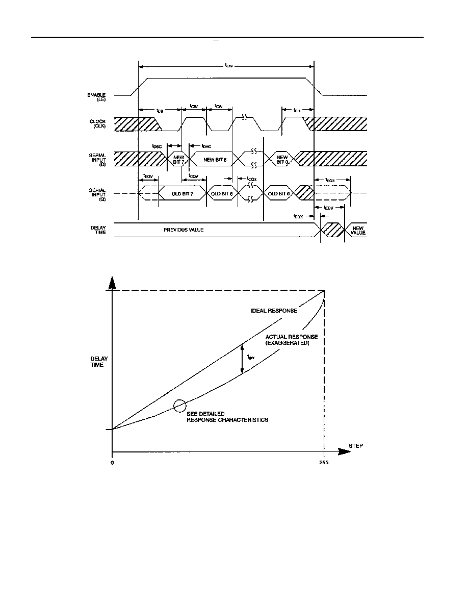
TIMING DIAGRAM: SERIAL MODE (
P
/S = 1)
Figure 12
DELAY vs PROGRAMMED VALUE
Figure 13
t
DO
t
DMAX
(measured)

DS1023
16 of 16
DETAILED RESPONSE CHARACTERISTICS
Figure 14
DELAY PARAMETERS
Figure 15
NOTES:
1. The device is trimmed such that t
DREF
= 255 * (nominal step size).
2. Since t
DO
is trimmed to be less than t
REF
, the actual step size will be slightly above the nominal value.
3. Consequently the range of absolute delay values (t
DMAX
-t
DO
) will also exceed the nominal range by an
amount equal to t
DREF0
.