
LTC4216
4216f
1
Allows Safe Board Insertion and Removal from
a Live Backplane
Controls Load Voltages from 0V to 6V
Fast Response Limits Peak Fault Current
Adjustable Analog Current Limit
Adjustable Soft-Start with Inrush Current Limiting
Adjustable Response Time for Overcurrent
Protection
Low Circuit Breaker Trip Threshold: 25mV
No External Gate Capacitor Required
Gate Drive for External N-Channel MOSFET
Adjustable Supply Voltage Power-Up Rate
RESET and FAULT Output
10-Lead MSOP and 12-Lead (4mm × 3mm) DFN
Packages
Ultralow Voltage
Hot Swap Controller
The LTC
®
4216 is a positive low-voltage Hot Swap
TM
controller that allows a board to be safely inserted and
removed from a live backplane. It controls load voltages
ranging from 0V to 6V and isolates a severe fault with
instantaneous analog current limiting.
An internal high side switch driver controls the gate of
an external N-channel MOSFET. An adjustable soft-start
limits the rate of change of the inrush current at start-up
for a large load capacitor. Together with an analog current
limit amplifi er, an electronic circuit breaker with adjustable
response time provides dual level overcurrent protection.
No external gate capacitor is required for the analog cur-
rent limit loop compensation.
The FB pin monitors the output supply voltage and signals
the RESET output pin. An ON pin provides on/off control
and a FAULT pin indicates the fault status. The LTC4216
is available in the 10-lead MSOP and 12-lead (4mm ×
3mm) DFN packages.
Single Channel 1.8V Hot Swap Controller
Electronic Circuit Breaker
Live Board Insertion and Removal
Industrial High Side Switch/Circuit Breaker
Optical Networking
Normal Power-Up
with Soft-Start
APPLICATIO S
U
FEATURES
DESCRIPTIO
U
TYPICAL APPLICATIO
U
4216 TA01b
0.5ms/DIV
V
GATE
5V/DIV
I
OUT
2.5A/DIV
V
OUT
1V/DIV
SENSEP SENSEN GATE
V
CC
ON
TIMER
FB
FAULT
RESET
SS
FILTER
LTC4216
330nF
20k
1%
17.4k
1%
10k
10k
1%
15k
1%
LONG
BACKPLANE
CONNECTOR
(FEMALE)
PCB EDGE
CONNECTOR
(MALE)
GND
LONG
SHORT
10nF
10nF
18nF
V
OUT
1.8V
5A
V
IN
1.8V
V
CC
3.3V
GND
Si4864DY
0.004
22
3.3V
10k
+
1000
µF
FAULT
RESET
µP
LOGIC
4216 TA01
LONG
, LTC and LT are registered trademarks of Linear Technology Corporation.
Hot Swap is a trademark of Linear Technology Corporation.
All other trademarks are the property of their respective owners.

LTC4216
4216f
2
SYMBOL PARAMETER
CONDITIONS
MIN
TYP
MAX
UNITS
V
CC
Bias Supply Range
2.3
6
V
V
SENSEP
V
SENSEP
Supply Range
0
6
V
I
CC
Bias Supply Current
V
ON
= 2V, V
FB
= 2V
1.6 3
mA
V
CC(UVL)
Bias Supply Undervoltage Lockout
V
CC
Rising
1.97 2.12 2.23
V
V
CC(UVL,HYST)
Bias Supply Undervoltage
50
120 190
mV
Lockout
Hysteresis
V
CB(TH)
Circuit Breaker Trip Voltage Threshold
22.5
25
27.5
mV
(V
SENSEP
V
SENSEN
)
21.5 25 28.5 mV
V
ACL(TH)
Analog Current Limit Voltage Threshold
32 40 48 mV
(V
SENSEP
V
SENSEN
)
I
SENSEP(IN)
SENSEP Pin Input Current
V
SENSEP
= V
SENSEN
= V
CC
= 6V
20
70
250
µA
V
SENSEP
= V
SENSEN
= 0V, V
CC
= 6V
7 20
µA
I
SENSEN(IN)
SENSEN Pin Input Current
V
SENSEN
= V
SENSEP
= V
CC
= 6V
10 15
µA
V
SENSEN
= V
SENSEP
= 0V, V
CC
= 6V
5 10 15
µA
12
11
10
9
8
7
1
2
3
4
5
6
13
FAULT
V
CC
SENSEP
SENSEN
GATE
FB
RESET
ON
FILTER
TIMER
SS
GND
TOP VIEW
DE PACKAGE
12-LEAD (4mm
× 3mm) PLASTIC DFN
Bias Supply Voltage (V
CC
) ............................ 0.3V to 9V
Input Voltages
FB, ON, SS, SENSEP, SENSEN ................. 0.3V to 9V
TIMER, FILTER ............................ 0.3V to V
CC
+ 0.3V
Output Voltages
RESET, FAULT ......................................... 0.3V to 9V
GATE ...................................................... 0.3V to 15V
ORDER PART
NUMBER
DE PART*
MARKING
Consult LTC Marketing for parts specifi ed with wider operating temperature ranges.
*The temperature grade is indicated by a label on the shipping container.
4216
LTC4216CDE
LTC4216IDE
(Note 1)
The
denotes the specifi cations which apply over the full operating
temperature range, otherwise specifi cations are at T
A
= 25°C. V
CC
= 3.3V, unless otherwise noted. (Note 2)
Operating Temperature Range
LTC4216C ................................................ 0°C to 70°C
LTC4216I ............................................. 40°C to 85°C
Storage Temperature Range
MS ..................................................... 65°C to 150°C
DE ...................................................... 65°C to 125°C
Lead Temperature (Soldering, 10sec)
MS
Package
...................................................... 300°C
ORDER PART
NUMBER
MS PART*
MARKING
LTBKV
LTC4216CMS
LTC4216IMS
ELECTRICAL CHARACTERISTICS
ABSOLUTE AXI U
RATI GS
W
W
W
U
PACKAGE/ORDER I FOR ATIO
U
U
W
1
2
3
4
5
RESET
ON
FILTER
TIMER
GND
10
9
8
7
6
V
CC
SENSEP
SENSEN
GATE
FB
TOP VIEW
MS PACKAGE
10-LEAD PLASTIC MSOP
T
JMAX
= 125°C,
JA
= 160°C/W
T
JMAX
= 125°C,
JA
= 43°C/W,
JC
= 4.3°C/W
EXPOSED PAD (PIN 13)
INTERNALLY CONNECTED TO GND
(PCB CONNECTION OPTIONAL)

LTC4216
4216f
3
SYMBOL PARAMETER
CONDITIONS
MIN
TYP
MAX
UNITS
I
GATE(UP)
GATE Pull Up Current
Gate Drive On, V
GATE
= 0V, V
ON
= 2V
16 20 26
µA
I
GATE(DN)
GATE Pull Down Current
Gate Drive Off, V
GATE
= 5V, V
ON
= 0.6V
100
600 1500
µA
V
SENSEP
- V
SENSEN
= 55mV, V
GATE
= 5V
1
5
20
mA
V
SENSEP
- V
SENSEN
= 100mV, V
GATE
= 5V
15
50
100
mA
V
GATE
External N-Channel Gate Drive
2.3V V
CC
< 3V
4.0 5.0 7.9
V
(V
GATE
V
SENSEN
)
3V V
CC
6V
4.5 6.2 7.9
V
V
GATE(TH)
GATE Pin Threshold Voltage
V
GATE
Falling
0.15
0.2
0.3
V
V
SS(CLP)
SS Pin Clamp Voltage
After End of SS Timing Cycle
1.3 1.65 2.0
V
V
SS(TH)
SS Pin Threshold Voltage
V
SS
Falling
0.15 0.2 0.35
V
I
SS(UP)
SS Pull Up Current
V
ON
= 2V, V
SS
= 1.2V, V
FB
= 2V
7 10 13
µA
V
ON
= 2V, V
FB
= 0V
0.3
1
2
µA
I
SS(DN)
SS Pull Down Current
V
ON
= 0V, V
SS
=
2V
8 mA
V
FB(TH)
FB Pin Threshold Voltage
V
FB
Falling
0.593 0.602 0.611
V
V
FB(LINEREG)
FB Pin Threshold Line Regulation
2.3V V
CC
6V
0.2 3
mV
V
FB(HYST)
FB Pin Hysteresis
3
mV
I
FB(IN)
FB Pin Input Current
V
FB
= 1.2V, V
CC
= 6V
0
±1
µA
V
ON(TH)
ON Pin Threshold Voltage
V
ON
Rising
0.77 0.8 0.83
V
V
ON(HYST)
ON
Pin
Hysteresis
40
80
130
mV
V
ON(FC)
ON Pin Fault Clear Threshold Voltage
V
ON
Falling
0.36 0.4 0.44
V
I
ON(IN)
ON Pin Input Current
V
ON
= 1.2V, V
CC
= 6V
0
±1
µA
V
TMR(TH)
TIMER Pin Threshold Voltage
V
TIMER
Rising
1.216 1.253 1.291
V
V
TIMER
Falling
0.15 0.2 0.35
V
I
TMR(UP)
Timer Pull Up Current
Timer On, V
ON
= 2V, V
TIMER
= 1V
1.5
2
2.5
µA
I
TMR(DN)
Timer Pull Down Current
Timer Off, V
ON
= 0V, V
TIMER
=
2V
8 mA
V
FILT(TH)
FILTER Pin Threshold Voltage
V
FILTER
Rising
1.216 1.253 1.291
V
V
FILTER
Falling
0.15 0.2 0.35
V
I
FILT(UP)
Filter Pull Up Current
V
ON
= 2V, V
FILTER
= 1V, In Fault Mode
45 60 75
µA
I
FILT(DN)
Filter Pull Down Current
V
ON
= 2V, V
FILTER
= 1V, No Faults
1.5 2.4 3.3 µA
V
ON
= 0V, V
FILTER
= 2V, In Reset Mode
8
mA
V
FAULT(TH)
FAULT Pin Threshold Voltage
V
FAULT
Falling
1.216 1.253 1.291
V
V
FAULT(HYST)
FAULT Pin Hysteresis
10
mV
I
FAULT(UP)
FAULT Pin Current
V
ON
= 0V, V
FAULT
= 1.5V
3 5 7 µA
V
OL
Output Low Voltage (RESET, FAULT) I
RESET
= I
FAULT
= 1.6mA
0.15 0.4
V
I
RESET(LEAK)
RESET Pin Input Leakage Current
V
RESET
= V
CC
= 6V
0
±10
µA
t
CB(TRIP)
Circuit Breaker Trip to Gate
(V
SENSEP
- V
SENSEN
) = Step 0V to 30mV,
120
240
360
µs
Discharging
V
SENSEP
= V
CC
, FILTER = 10nF to GND
t
FAULT(EXT)
FAULT Low to Gate Discharging
V
FAULT
= Step 2V to 0V
10 20
µs
t
FILTER
FILTER High to Gate Discharging
V
FILTER
= Step 0V to 2V
20 40
µs
t
RST(ONLO)
Circuit Breaker Reset Delay Time,
V
ON
= Step 2V to 0V
30 60
µs
ON Low to FAULT High
t
RST(VCCLO)
Circuit Breaker Reset Delay Time,
V
ON
= 2V, V
CC
= Step 3.3V to 1.8V
50 100
µs
V
CC
Low to FAULT High
t
OFF
Turn-Off Time, ON Low to GATE Discharging
V
ON
= Step 2V to 0.6V
15
µs
The
denotes the specifi cations which apply over the full operating
temperature range, otherwise specifi cations are at T
A
= 25°C. V
CC
= 3.3V, unless otherwise noted. (Note 2)
ELECTRICAL CHARACTERISTICS
Note 1: Absolute Maximum Ratings are those values beyond which the life
of a device may be impaired.
Note 2: All currents into device pins are positive; all currents out of
the device pins are negative; all voltages are referenced to GND unless
otherwise specifi ed.

LTC4216
4216f
4
TEMPERATURE (
°C)
50
V
FB(TH)
(V)
125
4216 G09
25
0
25
50
75
100
0.611
0.608
0.605
0.602
0.599
0.596
FALLING
RISING
TEMPERATURE (
°C)
50
I
GATE(UP)
(
µ
A)
125
4216 G08
25
0
25
50
75
100
22
21
20
19
18
TEMPERATURE (
°C)
50
V
ACL(TH)
(mV)
125
4216 G07
25
0
25
50
75
100
42
41
40
39
38
TEMPERATURE (
°C)
50
V
CB(TH)
(mV)
125
4216 G04
25
0
25
50
75
100
27
26
25
24
23
V
SENSEN
(V)
0
V
GATE
(V)
14
12
10
8
6
4
2
1
2
3
4
4216 G06
5
6
V
CC
= 6V
TEMPERATURE (
°C)
50
V
GATE
(V)
125
4216 G05
25
0
25
50
75
100
7.0
6.5
6.0
5.5
5.0
4.5
V
CC
= 5V
V
CC
= 3.3V
V
SENSEP
= V
SENSEN
= V
CC
V
CC
= 2.5V
V
CC
(V)
2.0
I
CC
(mA)
6.0
4216 G01
2.5
3.0
3.5
4.0
4.5
5.0
5.5
3.0
2.5
2.0
1.5
1.0
0.5
TEMPERATURE (
°C)
50
I
CC
(mA)
125
4216 G02
25
0
25
50
75
100
3.0
2.5
2.0
1.5
1.0
0.5
V
CC
= 6V
V
CC
= 3.3V
V
CC
= 2.3V
TEMPERATURE (
°C)
50
V
CC(UVL)
(V)
125
4216 G03
25
0
25
50
75
100
2.20
2.15
2.10
2.05
2.00
1.95
1.90
FALLING
RISING
I
CC
vs V
CC
I
CC
vs Temperature
V
CC(UVL)
vs Temperature
V
CB(TH)
vs Temperature
V
GATE
vs Temperature
V
GATE
vs V
SENSEN
V
ACL(TH)
vs Temperature
I
GATE(UP)
vs Temperature
V
FB(TH)
vs Temperature
Specifi cations are at T
A
= 25°C. V
CC
= 3.3V,
unless otherwise noted.
TYPICAL PERFOR A CE CHARACTERISTICS
U
W

LTC4216
4216f
5
TEMPERATURE (
°C)
50
I
FILT(DN)
(
µ
A)
125
4216 G17
25
0
25
50
75
100
2.8
2.6
2.4
2.2
2.0
TEMPERATURE (
°C)
50
I
FILT(UP)
(
µ
A)
125
4216 G16
25
0
25
50
75
100
70
65
60
55
50
TEMPERATURE (
°C)
50
V
SS(CLP)
(V)
125
4216 G15
25
0
25
50
75
100
1.9
1.8
1.7
1.6
1.5
1.4
TEMPERATURE (
°C)
50
V
FILT(TH)
(V)
125
4216 G14
25
0
25
50
75
100
1.27
1.26
1.25
1.24
1.23
TEMPERATURE (
°C)
50
V
FAULT(TH)
(V)
125
4216 G12
25
0
25
50
75
100
1.27
1.26
1.25
1.24
1.23
TEMPERATURE (
°C)
50
V
ON(TH)
(V)
125
4216 G11
25
0
25
50
75
100
0.90
0.85
0.80
0.75
0.70
0.65
0.60
FALLING
RISING
TEMPERATURE (
°C)
50
V
TMR(TH)
(V)
125
4216 G10
25
0
25
50
75
100
1.27
1.26
1.25
1.24
1.23
TEMPERATURE (
°C)
50
I
SS(UP)
(
µ
A)
125
4216 G18
25
0
25
50
75
100
12
10
8
6
4
2
0
V
FB
= 2V
V
FB
= 0V
V
TMR(TH)
vs Temperature
V
ON(TH)
vs Temperature
V
FAULT(TH)
vs Temperature
I
TMR(UP)
vs Temperature
V
FILT(TH)
vs Temperature
V
SS(CLP)
vs Temperature
I
FILT(UP)
vs Temperature
I
FILT(DN)
vs Temperature
I
SS(UP)
vs Temperature
TYPICAL PERFOR A CE CHARACTERISTICS
U
W
TEMPERATURE (
°C)
50
I
TMR(UP)
(
µ
A)
125
4216 G13
25
0
25
50
75
100
2.2
2.1
2.0
1.9
1.8

LTC4216
4216f
6
RESET (Pin 1/Pin 1): Reset or Power-Good Output. Open
drain output that pulls low if the FB pin voltage falls below
its threshold (0.6V). If an undervoltage lockout condition
occurs, the RESET pin pulls low and ignores the FB pin
voltage.
ON (Pin 2/Pin 2): ON Control Input. A rising edge above
the ON pin threshold (0.8V) initiates the start-up cycle and
turns on the external N-channel MOSFET. A falling edge
below 0.72V (80mV ON pin hysteresis) turns it off. If this
pin is pulled below 0.4V, following a circuit breaker trip, it
resets the electronic circuit breaker and fault latch.
FILTER (Pin 3/Pin 3): Fault Filter Input. Connect a capacitor
between this pin and ground to set up the fault fi lter delay.
This pin sources 60µA or sinks 2.4µA when the voltage
across the sense resistor exceeds 25mV or drops below
25mV respectively.
TIMER (Pin 4/Pin 4): Timer Input. Connect a capacitor
between this pin and ground to set up the start-up timing
cycle duration. It also defi nes the RESET power-good delay
from the instant the FB pin voltage exceeds 0.6V. This pin
sources 2µA pull-up current during ramp up.
SS (Pin 5/Not Available): Soft-Start Control Input. Con-
nect a capacitor between this pin and ground for soft-start
during power-up. It controls the GATE ramp up, limiting
the rate of change of the inrush current when the external
MOSFET turns on. If soft-start function is not used, leave
this pin unconnected.
GND (Pin 6/Pin 5): Device Ground.
FB (Pin 7/Pin 6): Output Monitor for Reset Output. A resis-
tive divider from the external MOSFET's source terminal is
tied to this pin. When the voltage at this pin drops below
0.6V, the RESET pin pulls low.
GATE (Pin 8/Pin 7): Gate Drive for External N-Channel
MOSFET. An internal charge pump provides 20µA gate
pull-up current and suffi cient gate overdrive to the exter-
nal MOSFET. An internal shunt regulator limits the GATE
pin voltage to about 6.2V (typ) above the SENSEN pin
voltage.
SENSEN (Pin 9/Pin 8): Circuit Breaker Negative Sense
Input. Connect this pin to the sense resistor terminal wired
to the drain of the external N-channel MOSFET. The sense
resistor is placed in the power path between SENSEP and
SENSEN pins to sense the output current. The electronic
circuit breaker trips if the voltage across the sense resistor
exceeds 25mV for more than a fault fi lter delay.
SENSEP (Pin 10/Pin 9): Circuit Breaker Positive Sense
Input. Connect this pin to the sense resistor terminal wired
to the positive supply input for the external output load.
This positive supply range extends from 0V to 6V.
V
CC
(Pin 11/Pin 10): Bias Supply Input. Operates from
2.3V to 6V. An internal undervoltage lockout circuit disables
the device until the input supply voltage at V
CC
exceeds
2.12V typically.
FAULT (Pin 12/Not Available): Fault Input and Output. As
an input, driving this pin low (<1.253V) will latch-off the
device to fault mode. As an output, it is either pulled high
by an internal 5µA pull-up or an external pull-up resistor
to positive supply under normal operating condition. It
pulls low when the circuit breaker is tripped due to an
overcurrent fault.
Exposed Pad (Pin 13/Not Available): Exposed pad may
be left open or connected to device ground.
(DE12 Package/MS Package)
PI FU CTIO S
U
U
U

LTC4216
4216f
7
The LTC4216 is a Hot Swap controller residing either on
a removable circuit board or on the backplane. It moni-
tors the current and protects the load with an external
N-channel MOSFET and a current sensing resistor (see
Typical Application). Both inrush current limiting and
short-circuit protection are provided by the LTC4216. The
device is powered via the bias supply input (V
CC
) and it
has a separate sense pin, SENSEP, to monitor the load
supply (V
IN
). The load supply can extend from 0V to 6V,
with a minimum bias supply voltage of 2.3V.
When the ON pin is pulled from low to high, TIMER begins
the fi rst timing cycle by sourcing 2µA into C1 once these
conditions are met: bias supply voltage out of undervolt-
age lockout (> 2.12V); TIMER, SS, FILTER and GATE
pin voltages < 0.2V. When the C1 voltage rises above
the TIMER pin threshold (1.253V), TIMER pulls low and
releases both the SS and GATE pins. C2 starts to ramp
up at the SS pin, controlling the rate of GATE ramp. This
limits the rate of change of the inrush current fl owing into
the output load capacitance. RESET pin goes high after
the second timing cycle when the FB pin voltage exceeds
0.6V and its hysteresis.
When the external MOSFET is fully turned on, the output
will ramp to load supply voltage if the inrush into the load
capacitance is low. However, if the inrush current exceeds
the analog current limit of V
ACL(TH)
/R
SENSE
, the LTC4216
will ramp the output by sourcing the limited current into
the load capacitance.
The LTC4216 provides protection against output short-
circuits or current overload through an internal electronic
circuit breaker with trip threshold of 25mV and an analog
current limit circuit. The circuit breaker response time is
set by C3 at the FILTER pin.
+
+
+
+
+
+
+
+
+
+
0.2V
2.12V
0.4V
0.8V
0.6V
2
µA
2.4
µA
1.253V
CP1
CP6
CP7
CP5
CP4
V
CC
V
CC
V
CC
SENSEP
SENSEN
GATE
SS**
RESET
ON
FB
4216 BD
FAULT**
GND
TIMER
FILTER
NORMAL
UVLO
ECB
ACL
NOTE 1: FILTER DELAY IS SET BY FILTER PIN CAPACITOR
** ONLY AVAILABLE IN THE DE12 PACKAGE
V
CC
V
CC
CP2
CP3
1.253V
1.253V
6
µs
DELAY
FAULT LATCH
RESET
DEVICE
RESET
FAULT LATCH-OFF
OUT OF UVLO
CB TRIPS
OR UVLO
GATE
ON
GATE
OFF
M4
M3
M2
M1
M5
M6
R1
M7
M9
M10
M8
Z1
D1
D2
CHARGE
PUMP
100
µA
20
µA
40mV
25mV
10
µA
1
µA
5
µA
GATE ON
GATE OFF
DEVICE RESET, UVLO
OR POWER BAD
CB
TRIPS
FILTER
FUNCTION OF
OVERDRIVE
FILTER DELAY
(SEE NOTE 1)
30
µs
DELAY
60
µA
V
CC
LOGIC
3
µs
DELAY
+
+
BLOCK DIAGRA
W
OPERATIO
U

LTC4216
4216f
8
Hot Circuit Insertion
When circuit boards are inserted into a live backplane, the
supply bypass capacitors can draw huge transient current
from the power bus as they charge. Potentially, the fl ow
of current could damage the connector pins and glitch
the power bus, causing other boards in the system to
reset. The LTC4216 is designed to turn on or off a circuit
board supply in a controlled manner, allowing insertion
or removal without glitches or connector damage.
Overview of LTC4216 Features
1. Allows safe board insertion and removal from a live
backplane.
2. Controls load voltages from 0V to 6V.
3. High side gate drive for external N-channel MOSFET.
4. Adjustable soft-start with inrush current limiting for
large load capacitor during start-up.
5. Adjustable analog current limit (ACL) with circuit
breaker fault time-out during an overcurrent fault condi-
tion. No external gate capacitor is required for the ACL
loop compensation.
6. Electronic circuit breaker tripping at 25mV across the
sense resistor. The response time is adjustable through
an external capacitor at the FILTER pin.
7. Provides an ON pin to turn on and off the device. This
can also be used to reset the device after a circuit breaker
trip.
8. Provides output supply voltage monitoring through the
FB pin and signals the RESET pin output.
9. Provides fault status output.
ON Control
The ON pin has two hysteretic comparators with differ-
ent threshold levels (0.8V and 0.4V) and they serve two
purposes:
1. Turn on the device if the ON pin voltage > 0.8V for more
than 6µs and turn it off if the ON pin voltage < 0.72V for
more than 15µs.
2. Reset the device if the ON pin voltage < 0.4V for more
than 30µs after a circuit breaker trip.
There are various methods of setting the ON pin
voltage:
1. Tie the ON pin to the load supply (V
IN
) through a 10k
pull-up resistor.
2. Drive the ON pin with an ON/OFF logic signal from the
system controller.
3. Connect an external resistive divider at the ON pin.
This divider can be used to set a higher value for the load
supply undervoltage lockout voltage than the internal V
CC
undervoltage lockout circuit.
For example, as shown in Figure 17, if both V
CC
and
SENSEP pins are connected to a 5V load supply, choosing
the resistive divider values, R1 = 20k, R2 = 80.6k, turns on
the device when the load supply voltage reaches around
80% of its fi nal value.
V
CC
Undervoltage Lockout
A hysteretic comparator, UVLO, monitors bias supply (V
CC
)
for undervoltage. The thresholds are defi ned by V
CC(UVL)
(2.12V) and its hysteresis, V
CC(UVL,HYST)
(120mV).
When V
CC
rises above V
CC(UVL)
, the device is enabled.
When V
CC
falls below (V
CC(UVL)
V
CC(UVL,HYST)
), the
device is disabled and GATE is pulled low. If V
CC
cycles
below this threshold for more than 200µs, following a
circuit breaker trip, it clears the fault latch. Any bias sup-
ply glitches that last less than 10µs will be rejected by the
UVLO glitch fi lter.
Timer
An external capacitor, C1, is used at TIMER pin to provide
two timing cycles for the LTC4216. The fi rst timing cycle
is the debounce cycle when the ON pin is fi rst turned on,
both the GATE and SS pins are held low and any short-
circuit faults are ignored by the electronic circuit breaker.
Second timing cycle is the power-good delay before the
RESET pin goes high when the FB pin voltage exceeds
0.6V and its hysteresis.
The TIMER pin sources 2µA into C1 during the two timing
cycles and is then pulled low by an internal N-channel
APPLICATIO S I FOR ATIO
W
U
U
U

LTC4216
4216f
9
+
LOGIC
TIMER
TIMER
LTC4216**
SENSEP
0.6V
V
CC
V
IN
ON
FB
R4
R3
R
SENSE
R5
M2
M1
RESET
SENSEN
GATE
+
C1
C
LOAD
**ADDITIONAL DETAILS
OMITTED FOR CLARITY
RESET
µP
V
OUT
+
4216 F02
switch when the TIMER pin voltage exceeds its threshold.
The timer period for C1 to charge up to the TIMER pin
threshold, V
TMR(TH)
(1.253V), is given by:
t
V C
A
TIMER
=
1 253
1
2
.
·
µ
(1)
For example, if C1 = 10nF, t
TIMER
= 6.2ms.
FB Glitch Filtering
The FB pin is used to monitor the output voltage of the
external MOSFET through a resistive divider. Any tran-
sients on the FB pin due to the output low spikes will
pull RESET low. To prevent RESET from generating an
unwanted system reset, the FB comparator has a glitch
fi lter to ride out these glitches. The fi lter time is 20µs for
large transients (greater than 150mV) and up to 100µs
for small transients. The relationship between glitch fi lter
time and the FB pin transient voltage or FB overdrive is
shown in Figure 1.
FB pin voltage rises above 0.6V, the FB comparator output
goes low and a new timing cycle starts. After a complete
timing cycle at time point 6, RESET is pulled high by the
external pull-up resistor, R5. The timer period given by
Equation (1) sets the power-good delay for RESET going
high. If the FB pin voltage stays above 0.6V for less than
a timing cycle at time point 4, the RESET output remains
low. Any overcurrent fault detected by the electronic circuit
breaker or FAULT pin driven low externally during the
timing cycle, will also pull the TIMER pin low and RESET
output remains low.
When the device enters an undervoltage lockout condition
or the ON pin voltage drops below 0.4V, RESET is pulled
low, ignoring the FB pin voltage.
Figure 2. Output Voltage Monitor Block Diagram
Figure 3. Output Voltage Monitor
Waveforms in Normal Operation
1 2
V
OUT
V
TMR(TH)
V
FB
< 0.6V
V
FB
> 0.6V
V
FB
< 0.6V
V
FB
> 0.6V
TIMER
RESET
GLITCH FILTER DELAY
3
4
5
6
POWER-GOOD
DELAY
2µA
2µA
4216 F03
APPLICATIO S I FOR ATIO
W
U
U
U
Figure 1. FB Comparator Glitch Filter Time vs FB Overdrive
Output Voltage Monitor
As shown in Figure 2, the output voltage is monitored
through a resistive divider, R3 and R4, connected at the
FB pin, and a FB comparator with 0.6V threshold.
The normal operation of the output voltage monitor after a
start-up cycle is shown in Figure 3. At time point 1, when the
FB pin voltage falls below 0.6V, the FB comparator output
goes high. RESET is pulled low by an internal N-channel
switch after a glitch fi lter delay at time point 2. When the
FB OVERDRIVE (mV)
0
100
120
140
160
120
80
60
40
80
200
40
20
0
GLITCH FILTER TIME (
µ
s)
T
A
= 25
°C

LTC4216
4216f
10
Electronic Circuit Breaker
The LTC4216 features an electronic circuit breaker function
that protects the external MOSFET against short-circuits or
excessive load current conditions on the supply. An external
sense resistor connected between SENSEP and SENSEN
pins is used to measure the load current. If the voltage
across the sense resistor exceeds the circuit breaker trip
threshold of 25mV for more than a fault fi lter delay, the
gate of the MOSFET is pulled low, turning it off.
The fault fi lter delay is determined by a capacitor, C3, con-
nected between the FILTER pin and ground as in Equation
(2). The FILTER pin sources 60µA pull-up current when
the sense voltage across the sense resistor exceeds 25mV.
Otherwise, it pulls down with 2.4µA. When the FILTER
pin voltage exceeds V
FILT(TH)
threshold (1.253V), there
is an internal 20µs delay before the GATE pulls low and
the FAULT pin will be pulled low. If no FILTER capacitor
is used, the fi lter fault delay defaults to 20µs. The circuit
breaker response time or fault fi lter delay with the FILTER
capacitor, C3, is given by:
t
V C
A
s
CB TRIP
(
)
.
·
=
µ
+ µ
1 253
3
60
20
(2)
The FILTER capacitor, C3, should be chosen so that the
fault fi lter delay is not too short to trip the circuit breaker
as the MOSFET current charges up a large output load
capacitance in analog current limit during power-up. It
also should not be too long to exceed the safe operating
area (SOA) of the external MOSFET.
Intermittent overloads may exceed the current limit as in
Figure 5, but if the duration is suffi ciently short, the FILTER
pin voltage may not reach the V
FILT(TH)
threshold and the
device will not shut off. To handle this situation, the FILTER
discharges with 2.4µA whenever voltage across the sense
resistor is below 25mV. Any intermittent overload with
an aggregate duty cycle of more than 4% will eventually
trip the circuit breaker. Figure 6 shows the circuit breaker
response time in seconds normalized to 1µF as given by
Equation (3). The asymmetric charging and discharging
of FILTER is a fair gauge of MOSFET heating.
t
C
s
F
D
3
1 253
60
2 4
( /
)
.
(
· ) .
µ =
(3)
Following a circuit breaker trip, the device is latched-off
and FAULT is pulled low until the fault latch is cleared by
pulling the ON pin low (< 0.4V) for at least 100µs. The
FILTER pin is pulled low by an internal N-channel switch
to discharge the capacitor quickly when the ON pin volt-
age falls below 0.4V and pulls down with 2.4µA when the
ON pin voltage rises above 0.8V to initiate a new start-up
cycle. The new timing cycle will not start until the FILTER
pin voltage is below 0.2V. The electronic circuit breaker
is disabled during the fi rst timing cycle upon start-up and
any short-circuit faults will be ignored.
Figure 4. A Continuous Fault Timing
Figure 5. Multiple Intermittent Overcurrent Condition
V
FILTER
CIRCUIT BREAKER TRIPS
A
B
1.253V
NORMAL
MODE
FAULT
MODE
2.4µA
60µA
4216 F04
A1
I
LOAD
V
FILTER
V
GATE
CIRCUIT
BREAKER
TRIPS
1.253V
B1
CB
FAULT
CB
FAULT
CB
FAULT
A2
B2
A3
B3
25mV/R
SENSE
60µA
60µA
60µA
2.4µA
2.4µA
2.4µA
APPLICATIO S I FOR ATIO
W
U
U
U

LTC4216
4216f
11
Analog Current Limiting
In addition to an electronic circuit breaker, the LTC4216
has included a novel analog current limit (ACL) amplifi er
that does not require an external compensation capacitor
at the GATE pin. The amplifi er's stability is compensated
by the large gate input capacitance (C
ISS
) of the external
MOSFET used. These MOSFETs usually have C
ISS
1nF.
However, if the MOSFET's gate input capacitance (C
ISS
)
is too small for loop stability, then connect an external
capacitor between the GATE pin and ground to increase
the total gate capacitance to 1nF. As given by Equation
(4), the MOSFET current, I
ACL
, is limited to the analog
current limit voltage, V
ACL(TH)
, 40mV typical, across
the sense resistor, R
SENSE
, connected between SENSEP
and SENSEN pins.
I
V
R
ACL
ACL TH
SENSE
=
(
)
(4)
The V
ACL(TH)
threshold is 1.6 times higher than the
V
CB(TH)
threshold (25mV typical) to provide dual level cur-
rent sensing. When the ACL amplifi er servos the MOSFET
current at V
ACL(TH)
across the sense resistor, it exceeds
V
CB(TH)
threshold causing the FILTER pin to charge C3
with 60µA pull-up. If the condition persists long enough
for C3 to reach the V
FILT(TH)
threshold (1.253V), GATE is
pulled low and FAULT latched low.
If the voltage across the sense resistor is greater than
V
ACL(TH)
during an overload condition, the ACL amplifi er
will servo GATE downwards in an attempt to control the
MOSFET current. Since the GATE pin voltage overdrives
the MOSFET in normal operation, the ACL amplifi er needs
time to discharge the GATE to the threshold of the MOSFET
for gate regulation. For mild overload, the ACL amplifi er
can control the MOSFET current, but in the event of a
severe overload, the MOSFET current may overshoot as
the MOSFET has large GATE overdrive initially. The GATE
is quickly discharged to ground followed by the ACL ampli-
fi er taking control. For applications that require very fast
analog current limit recovery from the GATE undershoot as
it discharges, connect a series resistor, R
Z
, with an external
capacitor, C
Z
, at the GATE pin as shown in Figure 17.
Soft-Start
The LTC4216 features a soft-start function that controls
the di/dt of the inrush current during power-up. As large
output load capacitors are commonly used in low-voltage
applications, the normal inrush can be large enough to
glitch the load supply. With the soft-start function, the
gate of the external MOSFET is allowed to turn on very
gradually to control the inrush current fl owing into the
load capacitor without causing a supply glitch.
With an external capacitor, C2, connected between the SS
pin and ground, the GATE is servoed by the ACL amplifi er
to track the rate of SS ramp-up during power-up. There
are two slopes in the SS ramp-up profi le: 10µA current
source pull-up for a normal ramp rate; and 1µA current
source pull-up for a slower ramp rate. Both the SS ramp
rates are given as follows:
Normal SS Ramp Rate:
dV
dt
A
C
SS NOM
(
)
= µ
10
2
(5)
Slower SS Ramp Rate:
dV
dt
A
C
SS SLOW
(
)
= µ
1
2
(6)
Figure 6. Circuit Breaker Filter
Response for Intermittent Overload
APPLICATIO S I FOR ATIO
W
U
U
U
OVERLOAD DUTY CYCLE, D (%)
0
20
40
60
80
100
NORMALIZED RESPONSE TIME (s/
µ
F)
1
0.1
0.01
4216 F06
t/C3(s/
µF) = 1.253/[(60 · D) 2.4]

LTC4216
4216f
12
For example if C
nF
dV
dt
V ms and
dV
dt
V ms
SS NOM
SS SLOW
,
,
/
.
/
.
(
)
(
)
2
10
1
0 1
=
=
=
After the initial timing cycle, the SS capacitor is charged
by a 10µA current source pull-up and GATE is held low
by the ACL amplifi er. As SS ramps up, the ACL amplifi er
releases the GATE when it crosses its input offset volt-
age. At this instant, SS switches the pull-up current from
10µA to 1µA for a slower ramp rate. GATE continues to
charge up with 20µA pull-up before the MOSFET reaches
its turn-on threshold voltage. When the external MOSFET
is fi rst turned on, there is always a current step due to the
high gain of the MOSFET. The slower SS ramp rate allows
the gate of the external MOSFET to be turned on with a
smaller inrush current step.
When the external MOSFET is turned on, load current starts
to fl ow through the sense resistor, developing a voltage drop
across it. This allows the ACL amplifi er to servo the GATE
to the voltage across the sense resistor, thus controlling
the rate of change of the inrush current. At this instant, SS
switches back from 1µA to 10µA current source pull-up
for a normal ramp rate. GATE continues to ramp up as
the ACL amplifi er servos to track the SS ramp rate. At the
end of SS ramp-up when SS reaches its fi nal value, GATE
is servoed to V
ACL(TH)
across the sense resistor. If the
voltage across the sense resistor drops below V
ACL(TH)
due to a falling load current, the ACL amplifi er shuts off
and GATE ramps further by a 20µA pull-up.
SS is pulled low under any of the following conditions:
in V
CC
undervoltage lockout condition, during the fi rst
timing cycle or when the circuit breaker fault times out.
If the soft-start function is not used, leave the SS pin
unconnected.
Inrush Control with GATE Capacitor
For applications not requiring soft-start to control the
di/dt of the inrush current during power-up, an alternative
way to limit the inrush is to control the GATE pin voltage
slew rate by connecting an external capacitor, C4, from
the GATE pin to ground, as shown in Figure 7. The GATE
slew rate is given by:
dV
dt
A
C
C
GATE
GATE
=
µ
+
20
4
(7)
where C
GATE
is the associated parasitic GATE capacitance
due to the external MOSFET's gate input capacitance,
C
ISS
.
The inrush current fl owing into the load capacitor, C
LOAD
,
is limited to:
I
C
dV
dt
C
C
C
A
INRUSH
LOAD
GATE
LOAD
GATE
=
=
+
µ
·
·
4
20
(8)
For example, if C
LOAD
= 4700µF, C4 = 33nF and C
GATE
=
5nF, I
INRUSH
= 2.5A.
If C
LOAD
is very large and I
INRUSH
exceeds the analog
current limit, the GATE is servoed to control the inrush
current to V
ACL(TH)
/R
SENSE
.
One limitation with this technique is that it slows down
the system turn-on and turn-off time by adding a capaci-
tor at the GATE pin. Should this technique be used, C4
50nF is recommended. However, having an external gate
capacitor helps to eliminate voltage spikes coupled through
the MOSFET's drain-to-gate capacitance to the GATE pin
when the supply power is fi rst applied.
Figure 7. Inrush Control with External Gate Capacitor
SENSEP SENSEN GATE
FB
C4
**ADDITIONAL DETAILS
OMITTED FOR CLARITY
LTC4216**
R4
R3
R
SENSE
V
IN
V
OUT
M1
+
C
LOAD
4216 F07
APPLICATIO S I FOR ATIO
W
U
U
U

LTC4216
4216f
13
Normal Power-Up and Power-Down
Figure 8 illustrates the timing diagram for a normal power-
up sequence in the case where a printed circuit board is
inserted into a live backplane.
At time point 1, the bias supply (V
CC
) ramps up and en-
ables the device when the supply voltage rises above the
undervoltage lockout threshold (2.12V). At time point 2,
SENSEP supply, together with the ON pin, ramp up and
start the fi rst timing cycle when the ON pin voltage exceeds
0.8V. The TIMER capacitor is allowed to ramp up with 2µA
pull-up once all these conditions are met: GATE < 0.2V,
FILTER < 0.2V, TIMER < 0.2V, SS < 0.2V. At time point 3,
TIMER reaches the V
TMR(TH)
threshold and the fi rst timing
cycle terminates. The electronic circuit breaker is enabled
and TIMER capacitor is quickly discharged. At time point
4 checks are made for TIMER, GATE, FILTER and SS <
0.2V, V
SENSE
below 25mV and FAULT high before a GATE
ramp-up cycle begins. GATE is held low by the analog cur-
rent limit amplifi er as SS capacitor ramps up with a 10µA
current source. SS switches to 1µA pull-up for a slower
ramp rate when it crosses the input offset voltage of the
ACL amplifi er. At this time point, the ACL amplifi er releases
the GATE and allows it to ramp up with a 20µA pull-up. At
time point 6, when the GATE voltage reaches the turn-on
threshold of the external MOSFET, current begins fl owing
into the load capacitor. The MOSFET current level at this
time point is controlled by the ACL amplifi er and the GATE
ramp is slowed down. SS switches the pull-up current
from 1µA to 10µA for a normal ramp rate. Between time
points 6 and 7, the ACL amplifi er servos the GATE voltage
to track the SS ramp rate, limiting the slew rate of the load
current. At time point 7, SS reaches its fi nal value and
GATE continue to ramp up with the 20µA pull-up if the load
current is not in analog current limit. At time point 8, the
FB pin voltage exceeds 0.6V and the second timing cycle
is started. When the conditions of TIMER < 0.2V, V
SENSE
< 25mV and FAULT high are met, the TIMER capacitor is
allowed to ramp up. When TIMER reaches the V
TMR(TH)
threshold at time point 9, RESET goes high, indicating to
the system controller that power is good. After this, the
TIMER is held low.
When the ON pin voltage falls below (V
ON(TH)
V
ON(HYST)
)
threshold (0.72V), it initiates a power-down sequence. At
time point 11, GATE is discharged by both the ACL ampli-
fi er and a 100µA current source pull-down, causing the
output voltage to fall gradually. When the FB pin voltage
falls below 0.6V at time point 12, RESET goes low after a
glitch fi lter delay (see the section on FB glitch fi ltering),
indicating that power is bad. When the ON pin voltage falls
below 0.4V, the device resets and GATE is pulled low by a
strong pull-down device.
Soft-Start with Analog Current Limiting
When a very large output load capacitor is connected
during soft-start, the GATE voltage is servoed to regulate
the inrush current to V
ACL(TH)
/R
SENSE
. This is illustrated
in the timing diagram of Figure 9. After the initial timing
cycle, the GATE is allowed to ramp up, tracking the SS
ramp rate between time points 5 and 8. At time point 7,
when the load current builds up as the GATE pin voltage
increases, the voltage across the sense resistor rises above
V
CB(TH)
(25mV typical). The FILTER capacitor starts to
charge up by a 60µA current source pull-up. At time point
8, SS reaches its fi nal value at the end of SS ramp cycle.
This allows the GATE to be regulated by the ACL amplifi er
at V
ACL(TH)
(40mV typical) across the sense resistor,
R
SENSE
, limiting the inrush to:
I
mV
R
LIMIT
SENSE
=
40
(9)
The FILTER pin voltage continues to rise as the load ca-
pacitor charges up with the limited load current. At time
point 9, the FB pin voltage exceeds 0.6V, but the second
timing cycle is not allowed to start as the voltage across
the sense resistor exceeds 25mV. At time point 10, the load
current falls as the load capacitor is near full charge and
the voltage across the sense resistor drops below 40mV.
The analog current limit loop shuts off and the GATE ramps
further till its fi nal value. The FILTER capacitor discharges
by a 2.4µA pull-down when the voltage across the sense
resistor falls below 25mV at time point 11. The duration
between time points 7 and 11 must be shorter than one
circuit breaker delay, as given by Equation (2), to avoid
a fault time-out during GATE ramp-up for very large load
APPLICATIO S I FOR ATIO
W
U
U
U

LTC4216
4216f
14
Figure 8. Normal Power-Up/Power-Down Sequence
capacitors. A second timing cycle starts at time point 11
when the FB pin voltage exceeds 0.6V and the voltage
across the sense resistor drops below 25mV. RESET goes
high at the end of the second timing cycle (time point 12)
when TIMER reaches the V
TMR(TH)
threshold.
SENSEP
ON
TIMER
SS
GATE
V
OUT
RESET
V
CC
POWER GOOD
V
FB
> 0.6V
POWER BAD
V
FB
< 0.6V
(V
GATE
V
OUT
) > V
GS(TH)
V
TMR(TH)
V
TMR(TH)
TRACKS SS RAMP
20µA
2µA
2µA
0.72V
0.4V
0.8V
10µA
10µA
1µA
1 2
3
4
5 6
7 8
9
CHECK FOR GATE,
FILTER, TIMER,
SS < 0.2V
CHECK FOR GATE, FILTER,
TIMER, SS < 0.2V AND FAULT HIGH
10 11 12
13
PLUG-IN CYCLE
FIRST TIMING CYCLE
POWER-GOOD DELAY
SECOND TIMING CYCLE
4216 F08
START
GATE
RAMP
ELECTRONIC CIRCUIT
BREAKER ARMED
RESET GOES HIGH
IN
RESET
MODE
ON GOES LOW
RESET PULLED LOW
DUE TO POWER BAD
START 2ND TIMING CYCLE
(CHECK TIMER < 0.2V AND
FAULT HIGH)
APPLICATIO S I FOR ATIO
W
U
U
U

LTC4216
4216f
15
Figure 9. Normal Power-Up Sequence (with Analog Current Limiting)
SENSEP
ON
TIMER
SS
GATE
V
OUT
I
LOAD
FILTER
RESET
V
CC
POWER GOOD
V
FB
> 0.6V
LOAD CURRENT REGULATING
AT 40mV/R
SENSE
POWER BAD
V
FB
< 0.6V
(V
GATE
V
OUT
) > V
GS(TH)
(V
SENSEP
V
SENSEN
) > 25mV
FILTER RAMPS UP WHEN (V
SENSEP
V
SENSEN
) > 25mV
OUTPUT IN ANALOG CURRENT LIMIT,
(V
SENSEP
V
SENSEN
) = 40mV
(V
SENSEP
V
SENSEN
) < 25mV
TRACKS SS RAMP
IN REGULATION
20µA
60µA
2.4µA
V
TMR(TH)
2µA
V
TMR(TH)
2µA
10µA
10µA
1µA
CHECK FOR GATE,
FILTER, TIMER,
SS < 0.2V
CHECK FOR GATE, FILTER, TIMER, SS < 0.2V AND FAULT HIGH
PLUG-IN CYCLE
FIRST TIMING CYCLE
POWER-GOOD DELAY
SECOND TIMING CYCLE
4216 F09
1 2
3
4
5 6
7 8
9 10 11
12
16
15
14
13
0.72V
0.4V
0.8V
ELECTRONIC CIRCUIT BREAKER ARMED
RESET
GOES HIGH
IN RESET
MODE
(ON < 0.4V)
ON GOES LOW
(ON < 0.72V)
OUTPUT NO LONGER
IN CURRENT LIMIT
RESET PULLED LOW
DUE TO POWER BAD
2ND TIMING CYCLE CANNOT START WITH
OUTPUT IN ANALOG CURRENT LIMIT
V
FILT(TH)
APPLICATIO S I FOR ATIO
W
U
U
U

LTC4216
4216f
16
Power-Up into an Output-Short
Figure 10 shows the timing diagram in the case when the
output is a dead short during power-up. As GATE ramps
up at time point 6, the MOSFET current increases due to
the output short causing the voltage drop across the sense
resistor to rise above 25mV. FILTER sources 60µA, charg-
ing the external capacitor. At time point 7, GATE regulates
to limit the output current to 40mV/R
SENSE
. If the output
continues to be in analog current limit when the FILTER
pin voltage reaches its threshold (1.253V) at time point
8, the circuit breaker trips and GATE is pulled low. The
device latches-off and FAULT is pulled low, indicating a
fault condition. The FILTER capacitor discharges through
a 2.4µA pull-down until the device resets.
Resetting the Electronic Circuit Breaker
When the LTC4216's electronic circuit breaker is tripped
during a fault condition, FAULT is asserted low and the
RESET, SS and GATE pins are all pulled to ground. This is
shown in the timing diagram of Figure 11. The LTC4216
remains latched-off until the external fault is cleared. To
clear the internal fault latch and restart the device, pull
the ON pin low (< 0.4V) at time point 4 for at least 100µs,
after which the FAULT will go high at time point 5. Tog-
gling the ON pin from low to high (> 0.8V) initiates a new
start-up cycle.
Sense Resistor Considerations
The circuit breaker trip threshold of 25mV and the value of
the sense resistor, R
SENSE
, connected between the SENSEP
and SENSEN pins, determine the trip current level as given
by Equation (10). If the fault current level exceeds the
analog current limit, the current is limited to a value given
by Equation (11). Should the overload condition exist for
more than one fault fi lter delay as given by Equation (2),
the circuit breaker trips and the device is latched-off.
I
V
R
mV
R
TRIP CB
CB TH
SENSE
SENSE
(
)
(
)
=
=
25
(10)
I
V
R
mV
R
ACL
ACL TH
SENSE
SENSE
=
=
(
)
40
(11)
For a new circuit design, the sense resistor value is fi rst
calculated from the maximum operating load current under
normal conditions and the minimum circuit breaker trip
threshold. This is given by:
R
V
I
mV
I
SENSE
CB TH MIN
LOAD MAX
LOAD MAX
=
=
(
,
)
(
)
(
)
.
21 5
(12)
Figure 10. Power-Up into an Output-Short and
Circuit Breaker Trips
Figure 11. Mild Overcurrent Circuit Breaker Trips Followed by
Device Reset
TIMER
2.4
µA
2
µA
40mV
25mV
10
µA
10
µA
1
µA
1
2 3
4 5 6 7
8
4216 F10
0.8V
TRACKS SS RAMP
FPD
60
µA
SENSEP-SENSEN
FILTER
SS
GATE
V
OUT
ON
FAULT
RESET
V
FILT(TH)
V
TMR(TH)
V
GATE
V
OUT
< V
GS(TH)
FAULT
FILTER
DELAY
GATE
REGULATING
2.4
µA
<40mV
25mV
4216 F11
FPD
60
µA
t
RST(ONLO)
V
FILT(TH)
SENSEP-SENSEN
FILTER
FAULT
RESET
SS
GATE
V
OUT
1
ON
0.4V
POWER BAD
V
FB
< 0.6V
2 3
4
5
MILD
OVERCURRENT
FAULT LATCH
RESET
CIRCUIT BREAKER TRIPS
AND LATCHED-OFF
RESET PULLED LOW
DUE TO POWER BAD
APPLICATIO S I FOR ATIO
W
U
U
U

LTC4216
4216f
17
For example, if I
LOAD(MAX)
= 5A, R
SENSE
= 4.3m. The
nearest standard value is 4m.
For proper circuit breaker operation, kelvin-sense PCB
connections between the sense resistor and the LTC4216's
SENSEP and SENSEN pins are strongly recommended.
Figure 12 illustrates the correct way of making connections
between the LTC4216 and the sense resistor. PCB layout
should be balanced and symmetrical to minimize wiring
errors. In addition, the PCB layout for the sense resistor
should include good thermal management techniques for
optimal sense resistor power dissipation.
The power rating of the sense resistor should accom-
modate the fault current level during analog current limit
so that the component is not damaged before the circuit
breaker trips.
Circuit Breaker Trip Current Calculation
For a selected R
SENSE
value, the typical load current that
trips the circuit breaker is given by:
I
V
R
mV
R
TRIP TYP
CB TH TYP
SENSE TYP
SENSE TYP
(
)
(
,
)
(
)
(
)
=
=
25
(13)
The minimum load current that trips the circuit breaker
is given by:
I
V
R
mV
R
TRIP MIN
CB TH MIN
SENSE MAX
SENSE MAX
(
)
(
,
)
(
)
(
)
.
=
=
21 5
(14)
Figure 12. Making PCB Connections to the Sense Resistor
TO
SENSEP
W
TO
SENSEN
TRACK WIDTH W:
0.03 PER AMPERE
ON 1OZ COPPER
CURRENT FLOW
TO LOAD
SENSE RESISTOR
CURRENT FLOW
TO LOAD
4216 F12
where
R
R
R
SENSE MAX
SENSE TYP
TOL
(
)
(
)
·
=
+
1
100
The maximum load current that trips the circuit breaker
is given by:
I
V
R
mV
R
TRIP MAX
CB TH MAX
SENSE MIN
SENSE MIN
(
)
(
,
)
(
)
(
)
.
=
=
28 5
where
(15)
R
R
R
SENSE MIN
SENSE TYP
TOL
(
)
(
)
·
=
1
100
For example, if a sense resistor of 4m ± 1% R
TOL
is used
for current sensing, the typical trip current, I
TRIP(TYP
) =
6.25A. From Equations (14) and (15), I
TRIP(MIN)
= 5.3A
and I
TRIP(MAX)
= 7.2A respectively.
For proper operation and to avoid tripping the circuit breaker
unnecessarily, the minimum trip current, I
TRIP(MIN)
, must
exceed the maximum operating load current of the circuit
connected to the output of the MOSFET.
MOSFET Selection
The external MOSFET switch must have adequate safe
operating area (SOA) to handle short-circuit conditions
before the circuit breaker trips. These considerations
take precedence over continuous drain current ratings. A
MOSFET with adequate SOA for a given application can
always handle the required drain current, but the opposite
may not be true. Consult the manufacturer's MOSFET
datasheet for safe operating area and effective transient
thermal impedance curves.
MOSFET selection is a 3-step process by assuming the
absence of a soft-start capacitor. First, R
SENSE
is chosen
and then the time required to charge the load capacitance
is determined. This timing, along with the maximum short-
circuit current and maximum load supply voltage, defi nes
an operating point that is checked against the MOSFET's
SOA curve.
In addition, consider three other key parameters:
APPLICATIO S I FOR ATIO
W
U
U
U

LTC4216
4216f
18
1. Maximum drain-to-source voltage, V
DS(MAX)
The V
DS(MAX)
rating must exceed the maximum load sup-
ply voltage including spikes and ringing.
2. Gate-to-source voltage, V
GS
, overdrive
The absolute maximum rating for V
GS
is typically ±8V for
"logic level" and "sub-logic level" MOSFETs.
3. Drain-to-source resistance, R
DS(ON)
The R
DS(ON)
should be low for low-voltage applications
to allow its drain-to-source voltage, V
DS(ON)
, to be a very
small percentage of the supply voltage.
To begin a design, fi rst specify the maximum operating load
current and load capacitance. Calculate the R
SENSE
value
from Equation (12). The minimum trip current, I
TRIP(MIN)
,
given by Equation (14) should be set to accommodate the
maximum operating load current.
During the start-up cycle, the LTC4216 may operate the
MOSFET in analog current limit, forcing V
ACL(TH)
between
32mV to 48mV across R
SENSE
. The minimum inrush current
given by Equation (16) is calculated using the minimum
V
ACL(TH)
and maximum R
SENSE
value.
I
V
R
mV
R
INRUSH MIN
ACL TH MIN
SENSE MAX
SENSE MAX
(
)
(
,
)
(
)
(
)
=
=
32
(16)
The maximum short-circuit current given by Equation (17)
is calculated using the maximum V
ACL(TH)
and minimum
R
SENSE
value.
I
V
R
mV
R
SHORT CIRCUIT MAX
ACL TH MAX
SENSE MIN
SENSE MIN
-
=
=
(
)
(
,
)
(
)
(
)
48
(17)
Select the FILTER capacitor, C3, based on the slowest
expected charging rate; otherwise, FILTER might time-out
before the load capacitor is fully charged. A value for C3
is calculated based on the maximum time it takes the load
capacitor, C
LOAD
, to charge to its maximum value of load
supply (V
IN(MAX)
). That time is given by:
t
C
V
I
CHARGE LOAD
LOAD
IN MAX
INRUSH MIN
(
)
(
)
(
)
·
=
(18)
Rearranging Equation (2) for the circuit breaker response
time, the FILTER capacitor, C3, is given by:
C
t
s
A
V
CHARGE LOAD
3
20
60
1 253
=
µ
µ
(
)·
.
(
)
(19)
Returning to Equation (2), the circuit breaker response time
is calculated with a chosen C3 and used in conjunction
with V
IN(MAX)
and I
SHORT-CIRCUIT(MAX)
to check the SOA
curves of a prospective MOSFET.
As a numerical design example for the Typical Application,
consider V
IN(MAX)
= 1.8V + 5%, maximum operating load
current = 5A, C
LOAD
= 1000µF. Equation (12) gives R
SENSE
= 4.3m. Choose R
SENSE
= 4m ± 1% tolerance. From
Equations (14) and (16), I
TRIP(MIN)
= 5.3A (> I
LOAD(MAX)
= 5A) and I
INRUSH(MIN)
= 7.9A respectively. Equation (19)
gives C3 = 10nF. To account for errors in C3, FILTER current
(60µA) and FILTER threshold (1.253V), the calculated value
should be multiplied by 1.5, giving the nearest standard
value of C3 = 18nF.
If a short-circuit occurs, a current of up to I
SHORT-
CIRCUIT(MAX)
= 12.1A will fl ow through the MOSFET for
400µs as dictated by C3 = 18nF in Equation (2). The
MOSFET must be selected based on this criterion and
checked against the SOA curve.
V
CC
Supply RC Network
The LTC4216 has two separate pins, V
CC
and SENSEP, for
supply input and sensing:
1. V
CC
pin for powering the internal circuitry.
2. SENSEP pin, together with the SENSEN pin, for sens-
ing the current fl owing from the load supply through the
external sense resistor and N-channel MOSFET to the
output load.
In most hot swap devices, V
CC
and SENSEP are one
common pin, providing the device's supply and external
MOSFET's current sensing. However, supply dips due to
output-shorts can potentially trigger the device into an
undervoltage lockout condition, causing the device to
disable and its internal latches to reset.
As bypass capacitors are not allowed on the powered
supply side of the external MOSFET switch residing on
APPLICATIO S I FOR ATIO
W
U
U
U

LTC4216
4216f
19
Figure 13. Connecting Transient Protection
Devices to the LTC4216's Load Supply Rail
the plug-in boards, the LTC4216 provides two separate
pins for bias supply input and load supply sensing. With
this confi guration, an RC network, R
Y
and C
Y
, shown in
Figure 13, can be used with the V
CC
pin to ride out supply
glitches during output-shorts or adjacent board shorts.
The RC network shown has a time constant of 7µs and
this is good enough for the supply to ride out most supply
glitches, preventing the device from entering an under-
voltage lockout condition unnecessarily or losing supply
temporarily. When V
CC
and SENSEP pins are connected
together, the R
Y
value should be chosen such that V
CC
pin
voltage is lower than SENSEP by 70mV; otherwise, part of
V
CC
pin current will be diverted through SENSEP pin.
This unique scheme of separating the device's supply input
and sensing also provides the fl exibility of operating the
load supply from ground to its supply rail with a minimum
bias supply voltage of 2.3V. For proper operation, the load
supply is required to be equal to or less than the bias sup-
ply voltage (maximum 6V).
Supply Transients Protection
There are two methods used in most applications to
eliminate supply transients:
1. Transient voltage suppressor to clip the transient to
a safe level.
2. Snubber (series RC) network.
For applications with load supply voltages of 3.3V or
higher, the ringing and overshoot during hot-swap-
ping or output-shorts can easily exceed the absolute
maximum rating of the LTC4216. To minimize the risk,
a transient voltage suppressor and snubber network
are highly recommended at the SENSEP pin. For ap-
plications with load supply voltages of 2.5V or below,
usually a snubber network is adequate to reduce the
supply ringing.
Figure 13 shows the connections of the supply tran-
sient protection devices, Z1, R
X
and C
X
, around the
LTC4216. The RC network, R
Y
and C
Y
, at the V
CC
pin
also serve as a snubber circuit for the load supply (V
IN
).
On the PCB layout, these transient protection devices
should be mounted very close to the LTC4216's load
supply rail using short lead lengths to minimize lead
inductance.
SENSEP SENSEN GATE
V
CC
GND
GND
FB
FILTER
TIMER
LTC4216**
C
Y
0.33
µF
C
X
0.1
µF
R4
R3
SS
C1
Z1
Z1: SMAJ6.0A
**ADDITIONAL DETAILS
OMITTED FOR CLARITY
C2
M1
C3
V
OUT
5V
C
LOAD
R
SENSE
R
Y
22
R
X
10
+
4216 F13
V
IN
5V
APPLICATIO S I FOR ATIO
W
U
U
U
Staggered Pins Connections
The LTC4216 can be used on either the backplane side of
the connector or a printed circuit board, and examples for
both are shown in Figure 14 and 15. Printed circuit board
edge connectors with staggered pins are recommended as
the insertion and removal of circuit boards will sequence
the pin connections. Supplies (V
CC
and SENSEP) and
ground connections on the printed circuit board should
be wired to the long pins or blades of the edge connector.
Control signal (ON) and status signals (RESET and FAULT)
passing through the edge connector should be wired to
short pins or blades.
Backplane and PCB Connection Sensing
The LTC4216's ON pin can be used in various ways to
detect whether the printed circuit board is seated properly
in the backplane connector before the LTC4216 begins a
start-up cycle.
An example is shown in Figure 14, in which the LTC4216
is mounted on the PCB and the R1/R2 resistive divider
is connected to the ON pin. On the edge connector, R2
is wired to a short pin. Before the connectors are mated,
the ON pin is held low by R1, keeping the LTC4216 in an
off state. When the connectors are mated, the resistive
divider is connected to the load supply (V
IN
) and the ON
pin voltage rises above 0.8V, turning the LTC4216 on.

LTC4216
4216f
20
An example with LTC4216 mounted on the backplane is
shown in Figure 15. In this case, the NPN transistor, Q1,
and two resistors, R7 and R8, form the PCB connection
sensing circuit with the ON pin. With the PCB out of the
backplane connector, Q1 base is tied to load supply through
R7, turning Q1 on and pulling the LTC4216's ON pin low.
The base of Q1 is also wired to the backplane connector
pin. When the PCB is inserted into the backplane, Q1 base
is grounded through a short pin connection on the PCB.
This turns off Q1 and the LTC4216's ON pin is allowed to
pull high to the load supply through R8, turning it on.
In the previous examples, the PCB connection sensing
circuits are not wired with interrupt capability from the
system controller. As shown in Figure 16, adding logic-
level discrete N-channel MOSFETs, M2 and M3, and a
couple of resistors allow interrupt control to the sensing
circuit. M2 is held on by its gate, pulling high through
R8 to the load supply until the PCB is mated fi rmly to
the backplane connector. A low logic-level for both the
ON/RST and ON/OFF signals turns M2 and M3 off, allowing
the ON pin to be pulled high and turning LTC4216 on. A
high logic-level for the ON/OFF signal turns off the device
and pulls the GATE low. The device is reset by pulling the
ON/RST signal high.
5V Hot Swap Application
Figure 17 shows a hot swap application circuit with V
CC
and SENSEP pins connected together to a 5V load supply
(V
IN
). The resistive divider, R1/R2, sets the undervoltage
threshold for the load supply and allows the system to
start up only after the supply voltage rises above 4V. The
resistive divider, R3/R4, monitors V
OUT
and signals the
APPLICATIO S I FOR ATIO
W
U
U
U
Figure 14. Single Channel 1.5V Hot Swap Controller
Figure 15. Hot Swap Controller on Backplane with Staggered Pin Connections
SENSEP SENSEN GATE
TIMER
FB
FAULT
RESET
SS
FILTER
LTC4216
C
X
100nF
C4
10nF
R1
20k
1%
R4
13k
1%
R6
10k
R3
10k
1%
R2
3.3k
1%
LONG
BACKPLANE
CONNECTOR
(FEMALE)
PCB EDGE
CONNECTOR
(MALE)
GND
LONG
SHORT
C1
10nF
C2
10nF
C3
68nF
V
OUT
1.5V
5A
V
CC
3.3V
V
IN
1.5V
GND
M1
Si4864DY
R5
10k
+
C
LOAD
4700
µF
FAULT
RESET
µP
LOGIC
4216 F14
LONG
11
10
9
8
7
12
1
4
2
5
3
6
V
CC
PCB CONNECTION
SENSING
ON
C
Y
330nF
R
SENSE
0.004
R
Y
22
R
X
10
SENSEP SENSEN GATE
TIMER
FAULT
RESET
FB
SS
FILTER
LTC4216
C
Y
330nF
R6
10k
R9
100k
C
LOAD
1000
µF
V
OUT
3.3V
5A
R3
10k
1%
LONG
BACKPLANE
CONNECTOR
(FEMALE)
PCB EDGE
CONNECTOR
(MALE)
GND
LONG
SHORT
SHORT
SHORT
SHORT
C1
10nF
C2
4.7nF
C3
33nF
M1
Si4864DY
R7
10k
R5
10k
FAULT
RESET
4216 F15
11
10
9
8
7
12
1
4
5
3
6
Q1
2
V
CC
ON
R8
10k
+
R4
39.2k
1%
C
X
100nF
PCB
CONNECTION
SENSING
V
IN
3.3V
Z1
Z1: SMAJ6.0A
Q1: MMBT3904
R
SENSE
0.004
R
Y
22
R
X
10

LTC4216
4216f
21
RESET high when V
OUT
rises above 4.5V. Transient volt-
age suppressor, Z1, and snubber network, R
X
and C
X
,
connected at SENSEP pin are highly recommended to
protect the 5V supply system from ringing and voltage
spikes during a fault condition. The RC network, R
Y
and
C
Y
, connected at the V
CC
pin, allows the LTC4216 bias
supply to ride out supply glitches during a fault condition
or adjacent board shorts.
Auto-Retry after a Fault
As shown in Figure 18, the LTC4216 can be confi gured to
automatically retry after a fault condition by connecting
both the FAULT and ON pins together with an RC network.
The network has a pull-up resistor, R
AUTO
, tied to the load
supply (V
IN
) and an external capacitor, C
AUTO
, connected
to ground. The auto-retry circuit will attempt to restart
the LTC4216 after a circuit breaker trip, as shown in the
timing diagram of Figure 19. In addition to the cooling
cycle provided by the TIMER period during auto-retry
sequence, the RC time constant for the ON pin voltage to
reach 0.8V provides additional turn-off time to prevent
the external MOSFET from overheating. The auto-retry
duty cycle is given by:
Duty Cycle
t
t
t
t
t
t
SS
FILTER
OFF
TIMER
SS
FILTER
+
+
+
+
·
%
100
(20)
where
t
TIMER
= TIMER period as given by Equation (1);
t
OFF
= time taken to charge the capacitor, C
AUTO
, from
FAULT V
OL
to V
ON(TH)
threshold (0.8V). As there is an
internal 5µA current source pull-up at the FAULT pin, it
SENSEP SENSEN GATE
ON
TIMER
FB
FAULT
RESET
SS
11
10
9
8
7
12
1
4
2
5
3
6
FILTER
LTC4216
R1
5.62k
1%
R5
39.2k
1%
R7
10k
R4
10k
1%
R2
4.42k
1%
R3
20k 1%
R8
10k
C
Y
330nF
C
X
100nF
LONG
BACKPLANE
CONNECTOR
(FEMALE)
PCB EDGE
CONNECTOR
(MALE)
GND
LONG
SHORT
SHORT
SHORT
C1
10nF
C2
4.7nF
C3
33nF
V
OUT
3.3V
5A
V
IN
3.3V
ON/RST
ON/OFF
GND
M1
Si4864DY
R6
10k
+
C
LOAD
1000
µF
LONG
V
CC
5V
FAULT
RESET
µP
LOGIC
4216 F16
V
CC
Z1
M2
M3
Z1: SMAJ6.0A
M2, M3: 2N7002K
PCB CONNECTION SENSING
R
SENSE
0.004
R
Y
22
R
X
10
Figure 16. PCB Connection Sensing with ON/OFF Control
APPLICATIO S I FOR ATIO
W
U
U
U
SENSEP SENSEN GATE
ON
FB
FAULT
RESET
SS
11
10
9
8
7
12
1
4
2
5
3
6
FILTER
LTC4216
R4
64.9k
1%
R6
10k
R3
10k
1%
R1
20k
1%
C
Y
330nF
C
Z
10nF
C
X
100nF
R2
80.6k
1%
LONG
SHORT
LONG
BACKPLANE
CONNECTOR
(FEMALE)
PCB EDGE
CONNECTOR
(MALE)
GND
C1
10nF
C2
4.7nF
C3
22nF
V
OUT
5V
5A
V
IN
5V
GND
M1
Si4864DY
R5
10k
+
C
LOAD
470
µF
FAULT
RESET
µP
LOGIC
4216 F17
V
CC
Z1: SMAJ6.0A
TIMER
Z1
R
SENSE
0.004
R
Z
100
R
Y
22
R
X
10
Figure 17. 5V Hot Swap Application

LTC4216
4216f
22
TIMER
SENSEPSENSEN
SENSEP
FILTER
SS
2.4
µA
V
TMR(TH)
V
FILT(TH)
2
µA
V
TMR(TH)
2
µA
40mV
25mV
10
µA
10
µA
1
µA
1
2
3
4
6
7 8 9
0.4V
0.8V
V
OL
10
11 12
13
14
5
CHECK FOR GATE, FILTER,
TIMER, SS < 0.2V
CHECK FOR GATE, FILTER,
TIMER, SS < 0.2V AND FAULT HIGH
4216 F19
ON/FAULT
0.8V
ELECTRONIC CIRCUIT
BREAKER ARMED
OUTPUT IN ANALOG CURRENT LIMIT
ON/FAULT PULLED LOW
DEVICE RESET
1ST TIMING CYCLE RESTART
FILTER RAMPS UP WHEN
(V
SENSEP
V
SENSEN
) >25mV
GATE
(V
GATE
V
OUT
) > V
GS(TH)
TRACKS SS RAMP
GATE
REGULATING
60
µA
t
FILTER
t
SS
t
OFF
t
TIMER
t
RST(ONLO)
t
OFF
t
TIMER
Figure 19. Auto-Retry Timing
complicates the equation for t
OFF
. This is approximately
given by:
t
R
C
V
V
V
V
R
A
OFF
AUTO
AUTO
ON TH
OL
IN
ON TH
AUTO
-
+
µ
·
·(
)
(
)
·
(
)
(
)
5
(21)
t
FILTER
= circuit breaker response time as given by Equation
(2); t
SS
= approximated time taken to charge the soft-start
capacitor, C2, from 0V to its fi nal value (1.65V) by 10µA
current source only.
For the component values shown, the external RC time
constant is set at 0.2 second, t
TIMER
= 62ms, t
OFF
= 25ms
at V
IN
= 5V, t
SS
= 1.6ms, t
FILTER
= 480µs and the auto-retry
duty cycle is 2.3%. The auto-retry duty cycle can be further
reduced by increasing both the t
TIMER
delay and the RC
delay. As an example, increasing the TIMER capacitor, C1,
value from 100nF to 330nF, and R
AUTO
value from 200k
to 470k reduces the duty cycle to 0.8%.
APPLICATIO S I FOR ATIO
W
U
U
U
Figure 18. Auto-Retry Application
SENSEP SENSEN GATE
ON
FB
SS
11
10
9
8
7
12
1
4
2
5
3
6
FILTER
LTC4216
R3
10k
1%
R4
64.9k
1%
C
Y
330nF
C
X
100nF
R
AUTO
200k
C
AUTO
1
µF
R5
10k
LONG
SHORT
LONG
BACKPLANE
CONNECTOR
(FEMALE)
PCB EDGE
CONNECTOR
(MALE)
GND
C1
100nF
C2
4.7nF
C3
22nF
V
IN
5V
V
OUT
5V
5A
GND
M1
Si4864DY
+
C
LOAD
470
µF
V
CC
Z1: SMAJ6.0A
TIMER
Z1
FAULT
RESET
RESET
4216 F18
R
SENSE
0.004
R
Y
22
R
X
10
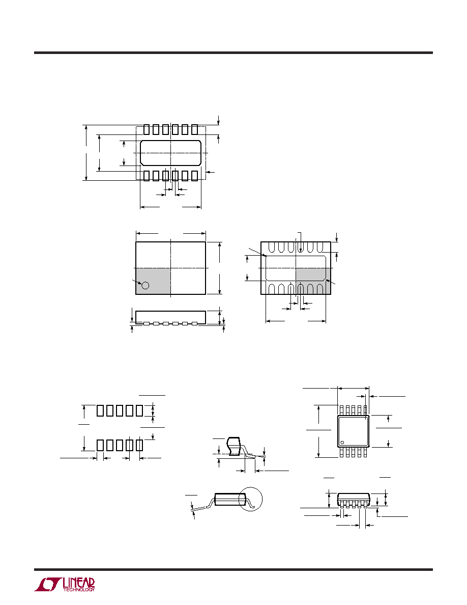
LTC4216
4216f
23
Information furnished by Linear Technology Corporation is believed to be accurate and reliable. However,
no responsibility is assumed for its use. Linear Technology Corporation makes no representation that
the interconnection of its circuits as described herein will not infringe on existing patent rights.
4.00
±0.10
(2 SIDES)
3.00
±0.10
(2 SIDES)
NOTE:
1. DRAWING PROPOSED TO BE A VARIATION OF VERSION
(WGED) IN JEDEC PACKAGE OUTLINE M0-229
2. DRAWING NOT TO SCALE
3. ALL DIMENSIONS ARE IN MILLIMETERS
4. DIMENSIONS OF EXPOSED PAD ON BOTTOM OF PACKAGE
DO NOT INCLUDE MOLD FLASH. MOLD FLASH, IF PRESENT,
SHALL NOT EXCEED 0.15mm ON ANY SIDE
5. EXPOSED PAD SHALL BE SOLDER PLATED
6. SHADED AREA IS ONLY A REFERENCE FOR PIN 1 LOCATION
ON THE TOP AND BOTTOM OF PACKAGE
0.38
± 0.10
BOTTOM VIEW--EXPOSED PAD
1.70
± 0.10
(2 SIDES)
0.75
±0.05
R = 0.115
TYP
R = 0.20
TYP
0.25
± 0.05
3.30
±0.10
(2 SIDES)
1
6
12
7
0.50
BSC
PIN 1
NOTCH
PIN 1
TOP MARK
(NOTE 6)
0.200 REF
0.00 0.05
(UE12/DE12) DFN 0603
0.25
± 0.05
3.30
±0.05
(2 SIDES)
RECOMMENDED SOLDER PAD PITCH AND DIMENSIONS
1.70
±0.05
(2 SIDES)
2.20
±0.05
0.50
BSC
0.65
±0.05
3.50
±0.05
PACKAGE OUTLINE
MSOP (MS) 0603
0.53
± 0.152
(.021
± .006)
SEATING
PLANE
0.18
(.007)
1.10
(.043)
MAX
0.17 0.27
(.007 .011)
TYP
0.127
± 0.076
(.005
± .003)
0.86
(.034)
REF
0.50
(.0197)
BSC
1 2 3 4 5
4.90
± 0.152
(.193
± .006)
0.497
± 0.076
(.0196
± .003)
REF
8
9
10
7 6
3.00
± 0.102
(.118
± .004)
(NOTE 3)
3.00
± 0.102
(.118
± .004)
(NOTE 4)
NOTE:
1. DIMENSIONS IN MILLIMETER/(INCH)
2. DRAWING NOT TO SCALE
3. DIMENSION DOES NOT INCLUDE MOLD FLASH, PROTRUSIONS OR GATE BURRS.
MOLD FLASH, PROTRUSIONS OR GATE BURRS SHALL NOT EXCEED 0.152mm (.006") PER SIDE
4. DIMENSION DOES NOT INCLUDE INTERLEAD FLASH OR PROTRUSIONS.
INTERLEAD FLASH OR PROTRUSIONS SHALL NOT EXCEED 0.152mm (.006") PER SIDE
5. LEAD COPLANARITY (BOTTOM OF LEADS AFTER FORMING) SHALL BE 0.102mm (.004") MAX
0.254
(.010)
0
° 6° TYP
DETAIL "A"
DETAIL "A"
GAUGE PLANE
5.23
(.206)
MIN
3.20 3.45
(.126 .136)
0.889
± 0.127
(.035
± .005)
RECOMMENDED SOLDER PAD LAYOUT
0.305
± 0.038
(.0120
± .0015)
TYP
0.50
(.0197)
BSC
MS Package
10-Lead Plastic MSOP
(Reference LTC DWG # 05-08-1661)
DE/UE Package
12-Lead Plastic DFN (4mm × 3mm)
(Reference LTC DWG # 05-08-1695)
PACKAGE DESCRIPTIO
U

LTC4216
4216f
24
Linear Technology Corporation
1630 McCarthy Blvd., Milpitas, CA 95035-7417
(408) 432-1900
FAX: (408) 434-0507
www.linear.com
© LINEAR TECHNOLOGY CORPORATION 2005
LT/TP 0205 1K · PRINTED IN USA
PART NUMBER
DESCRIPTION
COMMENTS
LTC1421
Dual Channels, Hot Swap Controller
Operates from 3V to 12V, Supports -12V, SSOP-24
LTC1422
Single Channel, Hot Swap Controller
Operates from 2.7V to 12V, SO-8
LTC1642
Single Channel, Hot Swap Controller
Operates from 3V to 16.5V, Overvoltage Protection up to 33V, SSOP-16
LTC1645
Dual Channel, Hot Swap Controller
Operates from 3V to 12V, Power Sequencing, SO-8 or SO-14
LTC1647-1/LTC1647-2/
Dual Channel, Hot Swap Controller
Operates from 2.7V to 16.5V, SO-8 or SSOP-16
LTC1647-3
LTC4210
Single Channel, Hot Swap Controller
Operates from 2.7V to 16.5V, Active Current Limiting, SOT23-6
LTC4211
Single Channel, Hot Swap Controller
Operates from 2.5V to 16.5V, Multifunction Current Control,
MSOP-8 or MSOP-10
LTC4212
Single Channel, Hot Swap Controller
Operates from 2.5V to 16.5V, Power-Up Timeout, MSOP-10
LTC4214
Negative Voltage, Hot Swap Controller
Operates from 6V to 16V, MSOP-10
LT4220
Positive and Negative Voltage,
Operates from ±2.7V to ±16.5V, SSOP-16
Dual Channels, Hot Swap Controller
LTC4221
Dual Hot Swap Controller/Sequencer
Operates from 1V to 13.5V, Multifunction Current Control, SSOP-16
LTC4230
Triple Channels, Hot Swap Controller
Operates from 1.7V to 16.5V, Multifunction Current Control, SSOP-20
TYPICAL APPLICATIO
U
RELATED PARTS
SENSEP SENSEN GATE
ON
FB
FILTER
LTC4216
R4
64.9k
1%
R3
10k
1%
C4
22nF
C
Y
330nF
C
X
100nF
R5
10k
LONG
SHORT
SHORT
LONG
BACKPLANE
CONNECTOR
(FEMALE)
PCB EDGE
CONNECTOR
(MALE)
GND
C1
10nF
C3
68nF
V
OUT
5V
2A
V
IN
5V
GND
M1
Si9426DY
+
C
LOAD
470
µF
4216 F20
V
CC
Z1: SMAJ6.0A
TIMER
Z1
RESET
RESET
R2
10k
R
SENSE
0.01
R
Y
22
R6
10
R
X
10
Figure 20. LTC4216CMS with Gate Capacitor for Slew Rate Control