Äîêóìåíòàöèÿ è îïèñàíèÿ www.docs.chipfind.ru
LTC3828
3828f
1
High Efficiency Dual 2.5V/3.3V Step-Down Converter with Tracking
FEATURES
DESCRIPTIO
U
APPLICATIO S
U
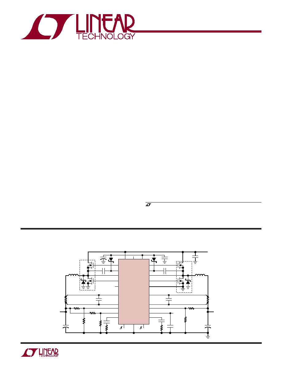
TYPICAL APPLICATIO
U
Dual, 2-Phase Step-Down
Controller with Tracking
Dual, 180
° Phased Controllers Reduce Required
Input Capacitance and Power Supply Induced Noise
Tracking for Both Outputs
Constant Frequency Current Mode Control
Wide V
IN
Range: 4.5V to 28V Operation
Power Good Output Voltage Indicator
Adjustable Soft-Start Current Ramping
Foldback Output Current Limiting
Disabled at Start-Up
No Reverse Current During Soft-Start Interval
Clock Output for 3-, 4-, 6-Phase Operation
Dual N-Channel MOSFET Synchronous Drive
±1% Output Voltage Accuracy
Phase-Lockable Fixed Frequency 260kHz to 550kHz
OPTI-LOOP
®
Compensation Minimizes C
OUT
Very Low Dropout Operation: 99% Duty Cycle
Output Overvoltage Protection
Small 28-Lead SSOP and 5mm
× 5mm QFN
Packages
The LTC
®
3828 is a dual high performance step-down
switching regulator controller that drives all N-channel
synchronous power MOSFET stages. A constant fre-
quency current mode architecture allows for a phase-
lockable frequency of up to 550kHz. The TRCKSS pin
provides both soft-start and tracking functions. Multiple
LTC3828s can be daisy-chained in applications requiring
more than two voltages to be tracked.
OPTI-LOOP
compensation allows the transient response
to be optimized over a wide range of output capacitance and
ESR values. The precision 0.8V reference and power good
output indicator are compatible with a wide 4.5V to 28V
(30V maximum) input supply range, encompassing all bat-
tery chemistries.
The RUN pins control their respective channels indepen-
dently. The FCB/PLLIN pin selects among Burst Mode
®
operation, skip-cycle mode and continuous current mode.
Current foldback limits MOSFET dissipation during short-
circuit conditions. Reverse current and current foldback
functions are disabled during soft-start.
Telecom Infrastructure
ASIC Power Supply
Industry Equipment
+
4.7
µF
0.1
µF
63.4k 1%
1000pF
3.2
µH
220pF
1
µF
CERAMIC
22
µF
50V
CERAMIC
+
47
µF
4V
SP
0.01
20k
1%
20k
1%
15k
3.3V
5A
0.1
µF
0.1
µF
0.1
µF
42.5k
1%
3.2
µH
220pF
1000pF
+
56
µF
4V
SP
0.01
20k
1%
15k
2.5V
5A
TG1
TG2
BOOST1
BOOST2
SW1
SW2
BG1
BG2
SGND
PGND
SENSE1
+
SENSE2
+
SENSE1
SENSE2
V
OSENSE1
V
OSENSE2
I
TH1
I
TH2
V
IN
PGOOD INTV
CC
RUN1
RUN2
4.5V TO 28V
3828 TA01
LTC3828
FCB/PLLIN
500kHz
TRCKSS1
TRCKSS1
TRCKSS2
63.4k 1%
, LTC and LT are registered trademarks of Linear Technology Corporation.
Burst Mode and OPTI-LOOP are registered trademarks of Linear Technology Corporation.
All other trademarks are the property of their respective owners.
Protected by U.S. Patents including 5481178, 5705919, 5929620, 6144194, 6177787,
6304066, 6580258
2
LTC3828
3828f
Input Supply Voltage (V
IN
)........................ 30V to 0.3V
Top Side Driver Voltages
(BOOST1, BOOST2) .................................. 36V to 0.3V
Switch Voltage (SW1, SW2) ........................ 30V to 5V
INTV
CC,
DRV
CC
, RUN1, RUN2, (BOOST1-SW1),
(BOOST2-SW2) .......................................... 7V to 0.3V
SENSE1
+
, SENSE2
+
, SENSE1
,
SENSE2
Voltages ....................... (1.1)INTV
CC
to 0.3V
FCB/PLLIN, PLLFLTR, CLKOUT,
PHSMD Voltage .............................. INTV
CC
to 0.3V
TRCKSS1, TRCKSS2 ........................... INTV
CC
to 0.3V
ABSOLUTE AXI U RATI GS
W
W
W
U
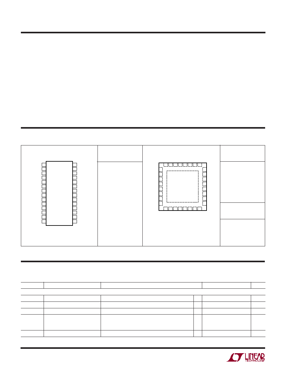
PACKAGE/ORDER I FOR ATIO
U
U
W
(Note 1)
PGOOD ..................................................... 5.5V to 0.3V
I
TH1,
I
TH2
, V
OSENSE1
, V
OSENSE2
Voltages ... 2.7V to 0.3V
Peak Output Current <10
µs (TG1, TG2, BG1, BG2) .. 3A
INTV
CC
Peak Output Current ................................ 50mA
Operating Temperature Range (Note 7)
LTC3828E .......................................... 40
°C to 85°C
Junction Temperature (Note 2) ............................ 125
°C
Storage Temperature Range ................ 65
°C to 125°C
Reflow Peak Body Temperature (UH Package) .... 260
°C
Lead Temperature (Soldering, 10 sec)
(GN Package) ................................................... 300
°C
ORDER PART
NUMBER
LTC3828EUH
T
JMAX
= 125
°C,
JA
= 34
°C/W
EXPOSED PAD IS SGND (PIN 33),
MUST BE SOLDERED TO PCB
The
denotes the specifications which apply over the full operating
temperature range, otherwise specifications are at T
A
= 25
°C. V
IN
= 15V, V
RUN1, 2
= 5V unless otherwise noted.
ELECTRICAL CHARACTERISTICS
SYMBOL
PARAMETER
CONDITIONS
MIN
TYP
MAX
UNITS
Main Control Loops
V
OSENSE1, 2
Regulated Feedback Voltage
(Note 3); I
TH1, 2
Voltage = 1.2V
0.792
0.800
0.808
V
I
VOSENSE1, 2
Feedback Current
(Note 3)
±5
±50
nA
V
REFLNREG
Reference Voltage Line Regulation V
IN
= 4.6V to 28V (Note 3)
0.002
0.02
%/V
V
LOADREG
Output Voltage Load Regulation
(Note 3)
Measured in Servo Loop;
I
TH
Voltage = 1.2V to 0.7V
0.1
0.5
%
Measured in Servo Loop;
I
TH
Voltage = 1.2V to 2.0V
0.1
0.5
%
g
m1, 2
Transconductance Amplifier g
m
I
TH1, 2
= 1.2V; Sink/Source 5uA; (Note 3)
1.3
mmho
Consult LTC Marketing for parts specified with wider operating temperature ranges.
UH PART
MARKING
3828
ORDER PART
NUMBER
LTC3828EG
T
JMAX
= 125
°C,
JA
= 95
°C/W
1
2
3
4
5
6
7
8
9
10
11
12
13
14
TOP VIEW
G PACKAGE
28-LEAD PLASTIC SSOP
28
27
26
25
24
23
22
21
20
19
18
17
16
15
CLKOUT
PGOOD
BOOST1
TG1
SW1
V
IN
INTV
CC
PGND
BG1
BG2
SW2
TG2
BOOST2
RUN2
TRCKSS1
I
TH1
SENSE1+
SENSE1
V
OSENSE1
PLLFLTR
RUN1
FCB/PLLIN
SGND
TRCKSS2
SENSE2
SENSE2
+
I
TH2
V
OSENSE2
32 31 30 29 28 27 26 25
9
10 11 12 13
TOP VIEW
33
14 15 16
17
18
19
20
21
22
23
24
8
7
6
5
4
3
2
1
V
OSENSE1
PLLFLTR
RUN1
PHSMD
FCB/PLLIN
SGND
TRCKSS2
NC
SW1
V
IN
INTV
CC
DRV
CC
PGND
BG1
BG2
SW2
SENSE1
SENSE1
+
I
TH1
TRCKSS1
CLKOUT
PGOOD
BOOST1
TG1
NC
SENSE2
SENSE2
+
I
TH2
V
OSENSE2
RUN2
BOOST2
TG2
UH PACKAGE
32-LEAD (5mm
× 5mm) PLASTIC QFN
LTC3828
3828f
3
The
denotes the specifications which apply over the full operating
temperature range, otherwise specifications are at T
A
= 25
°C. V
IN
= 15V, V
RUN1, 2
= 5V unless otherwise noted.
ELECTRICAL CHARACTERISTICS
SYMBOL
PARAMETER
CONDITIONS
MIN
TYP
MAX
UNITS
g
mGBW1, 2
Transconductance Amplifier GBW
I
TH1, 2
= 1.2V; (Note 3)
3
MHz
I
Q
Input DC Supply Current
(Note 4)
Normal Mode
V
IN
= 15V; V
OUT1
= 5V
2
3
mA
Shutdown
V
RUN/SS1, 2
= 0V
20
100
µA
V
FCB
Forced Continuous Threshold
0.76
0.800
0.84
V
I
FCB
Forced Continuous Pin Current
V
FCB
= 0.85V
0.50
0.18
0.1
µA
V
BINHIBIT
Burst Inhibit (Constant Frequency)
Measured at FCB pin
4.3
4.8
V
Threshold
UVLO
Undervoltage Lockout
V
IN
Ramping Down
3.5
4
V
V
OVL
Feedback Overvoltage Lockout
Measured at V
OSENSE1, 2
0.84
0.86
0.88
V
I
SENSE
Sense Pins Total Source Current
(Each Channel); V
SENSE1
, 2
= V
SENSE1
+
, 2
+
= 0V
90
65
µA
DF
MAX
Maximum Duty Factor
In Dropout
98
99.4
%
I
TRCKSS1,2
Soft-Start Charge Current
0.5
1.2
µA
V
RUN1, 2
ON
RUN Pin ON Threshold
V
RUN1,
V
RUN2
Rising
1.0
1.5
2.0
V
V
SENSE(MAX)
Maximum Current Sense Threshold
V
OSENSE1, 2
= 0.7V,V
SENSE1, 2
= 5V
62
75
85
mV
V
OSENSE1, 2
= 0.7V,V
SENSE1, 2
= 5V
60
75
88
mV
TG Transition Time:
(Note 5)
TG1, 2 t
r
Rise Time
C
LOAD
= 3300pF
55
100
ns
TG1, 2 t
f
Fall Time
C
LOAD
= 3300pF
55
100
ns
BG Transition Time:
(Note 5)
BG1, 2 t
r
Rise Time
C
LOAD
= 3300pF
65
120
ns
BG1, 2 t
f
Fall Time
C
LOAD
= 3300pF
55
100
ns
TG/BG t
1D
Top Gate Off to Bottom Gate On Delay
Synchronous Switch-On Delay Time
C
LOAD
= 3300pF Each Driver
60
ns
BG/TG t
2D
Bottom Gate Off to Top Gate On Delay
Top Switch-On Delay Time
C
LOAD
= 3300pF Each Driver
80
ns
t
ON(MIN)
Minimum On-Time
Tested with a Square Wave (Note 6)
120
ns
INTV
CC
Linear Regulator
V
INTVCC
Internal V
CC
Voltage
6V < V
IN
< 30V
4.8
5.0
5.2
V
V
LDO
INT
INTV
CC
Load Regulation
I
CC
= 0 to 20mA
0.2
2.0
%
Oscillator and Phase-Locked Loop
f
NOM
Nominal Frequency
V
PLLFLTR
= 1.2V
360
400
440
kHz
f
LOW
Lowest Frequency
V
PLLFLTR
= 0V
230
260
290
kHz
f
HIGH
Highest Frequency
V
PLLFLTR
2.4V
480
550
590
kHz
I
PLLFLTR
Phase Detector Output Current
Sinking Capability
f
PLLIN
< f
OSC
17
µA
Sourcing Capability
f
PLLIN
> f
OSC
17
µA
PGOOD Output
V
PGL
PGOOD Voltage Low
I
PGOOD
= 2mA
0.1
0.3
V
I
PGOOD
PGOOD Leakage Current
V
PGOOD
= 5V
±1
µA
V
PG
PGOOD Trip Level, Either Controller
V
OSENSE
with Respect to Set Output Voltage
V
OSENSE
Ramping Negative
6
7.5
9.5
%
V
OSENSE
Ramping Positive
6
7.5
9.5
%
4
LTC3828
3828f
OUTPUT CURRENT (A)
0.001
EFFICIENCY (%)
10
3828 G01
0.01
0.1
1
OUTPUT CURRENT (A)
0.001
10
0.01
0.1
1
100
90
80
70
60
50
40
30
20
10
0
EFFICIENCY (%)
3828 G02
100
90
80
70
60
50
INPUT VOLTAGE (V
5
EFFICIENCY (%)
100
90
80
70
60
50
25
3828 G03
10
15
20
30
TEMPERATURE (
°C)
50
3.8
3.6
3.4
3.2
3.0
100
3828 G06
25
0
25
50
75
125
UNDERVOLTAGE LOCKOUT (V)
INTV
CC
VOLTAGE (V)
3828 G05
INPUT VOLTAGE (V)
0
SUPPLY CURRENT (
µ
A)
1200
1000
800
600
400
200
0
5.2
5.0
4.8
4.6
4.4
4.2
4.0
5
10
15
20
3828 G04
25
30
INPUT VOLTAGE (V)
0
5
10
15
20
25
30
Burst Mode
OPERATION
FORCED
CONTINUOUS
MODE
CONSTANT
FREQUENCY
(BURST DISABLE)
V
OUT
= 5V
F = 260kHz
V
IN
=15V
V
OUT
= 5V
F = 260kHz
V
OUT
= 5V
I
OUT
= 3A
F = 260kHz
V
IN
= 7V
V
IN
= 20V
V
IN
= 15V
BOTH CONTROLLERS ON
SHUTDOWN
I
LOAD
= 1mA
Note 1: Absolute Maximum Ratings are those values beyond which the life
of a device may be impaired.
Note 2: T
J
is calculated from the ambient temperature T
A
and power
dissipation P
D
according to the following formulas:
LTC3828UH: T
J
= T
A
+ (P
D
· 34
°C/W)
LTC3828G: T
J
= T
A
+ (P
D
· 95
°C/W)
Note 3: The IC is tested in a feedback loop that servos V
ITH1, 2
to a
specified voltage and measures the resultant V
OSENSE1, 2.
Note 4: Dynamic supply current is higher due to the gate charge being
delivered at the switching frequency. See Applications Information.
Note 5: Rise and fall times are measured using 10% and 90% levels. Delay
times are measured using 50% levels.
Note 6: The minimum on-time condition is specified for an inductor
peak-to-peak ripple current
40% of I
MAX
(see minimum on-time
considerations in the Applications Information section).
Note 7: The LTC3828E is guaranteed to meet performance specifications
over the 40
°C to 85°C operating temperature range as assured by design,
characterization and correlation with statistical process controls.
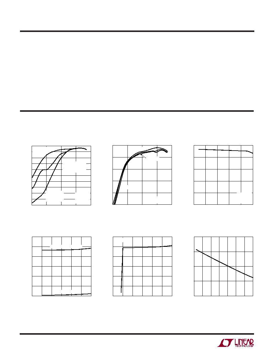
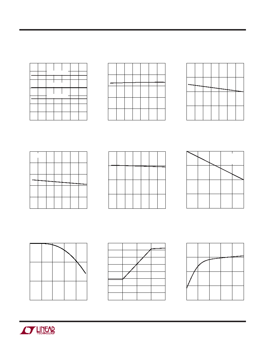
Efficiency vs Output Current
and Mode (Figure 14)
Efficiency vs Output Current
(Figure 14)
Efficiency vs Input Voltage
(Figure 14)
TYPICAL PERFOR A CE CHARACTERISTICS
U
W
ELECTRICAL CHARACTERISTICS
Internal 5V LDO Line Regulation
Undervoltage Lockout vs
Temperature
Supply Current vs Input Voltage
(Figure 14)
T
A
= 25
°C unless otherwise noted.
LTC3828
3828f
5
TEMPERATURE (
°C)
50
700
600
500
400
300
200
100
0
25
75
3828 G07
25
0
50
100
125
TEMPERATURE (
°C)
50
25
75
25
0
50
100
125
TEMPERATURE (
°C)
50
25
75
25
0
50
100
125
TEMPERATURE (
°C)
50
25
75
25
0
50
100
125
TEMPERATURE (
°C)
50
25
75
25
0
50
100
125
FREQUENCY (kHz)
TRCKSS CURRENT (
µ
A)
1.5
1.3
1.1
0.9
0.7
0.5
3828 G08
37
35
33
31
29
3828 G09
CURRENT SENSE INPUT CURRENT (
µ
A)
V
SENSE
(mV)
80
78
76
74
72
70
3828 G10
V
OUT
= 5V
5.1
5.0
4.9
4.8
4.7
3828 G11
INTV
CC
VOLTAGE (V)
LOAD CURRENT (A)
0
NORMALIZED V
OUT
(%)
0.2
0.1
4
3828 G12
0.3
0.4
1
2
3
5
0
FCB = 0V
V
IN
= 15V
FIGURE 14
DUTY FACTOR (%)
0
V
SENSE
(mV)
50
75
3828 G13
25
0
20
40
100
60
80
PERCENT ON NOMINAL OUTPUT VOLTAGE (%)
0
V
SENSE
(mV)
0.75
3828 G14
0.25
0.5
1.0
80
70
60
50
40
30
20
10
0
COMM0N MODE VOLTAGE (V)
0
V
SENSE
(mV)
70
75
4
3828 G15
65
60
1
2
3
5
80
V
PLLFLTR
= 2.4V
V
PLLFLTR
= 1.2V
V
PLLFLTR
= 0V
Oscillator Frequency vs
Temperature
TRCKSS Current vs Temperature
Current Sense Pin Input Current vs
Temperature
TYPICAL PERFOR A CE CHARACTERISTICS
U
W
Maximum Current Sense
Threshold vs Temperature
Load Regulation
INTV
CC
Voltage vs Temperature
T
A
= 25
°C unless otherwise noted.
Maximum Current Sense
Threshold vs Duty Factor
Maximum Current Sense
Threshold vs Percent of Nominal
Output Voltage (Foldback)
Maximum Current Sense
Threshold vs Sense Common
Mode Voltage