3819f.pm65
1
LTC3819
3819f
The LTC
®
3819 is a 2-phase, VID programmable, synchro-
nous step-down switching regulator controller that drives
two N-channel external power MOSFET stages in a fixed fre-
quency architecture. The 2-phase controller drives its two
output stages out of phase at frequencies up to 300kHz to
minimize the RMS ripple currents in both input and output
capacitors. The 2-phase technique effectively multiplies the
fundamental frequency by two, improving transient re-
sponse while operating each channel at an optimum fre-
quency for efficiency. Thermal design is also simplified.
An operating mode select pin (FCB) can be used to select
among three modes including Burst Mode
®
operation for
highest efficiency. An internal differential amplifier provides
true remote sensing of the regulated supply's positive and
negative output terminals as required in high current ap-
plications.
The RUN/SS pin provides soft-start and optional timed,
short-circuit shutdown. Current foldback limits MOSFET
dissipation during short-circuit conditions when the
overcurrent latchoff is disabled. OPTI-LOOP compensation
allows the transient response to be optimized for a wide
range of output capacitors and ESR values.
2-Phase, High Efficiency,
Step-Down Controller for
Sun Server CPUs
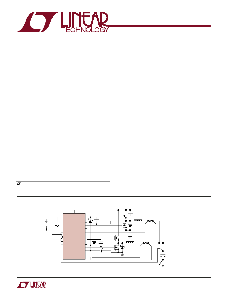
Figure 1. High Current Dual Phase Step-Down Converter
SunTM Server CPU Supply
Output Stages Operate Antiphase Reducing Input
and Output Capacitance Requirements and Power
Supply Induced Noise
Dual Input Supply Capability for Load Sharing
5-Bit SUN CPU VID Code:
V
OUT
= 1.025V to 1.4125V
±1% Output Voltage Accuracy
True Remote Sensing Differential Amplifier
Power Good Output Voltage Monitor
Supports Active Voltage Positioning
Current Mode Control Ensures Current Sharing
OPTI-LOOP
®
Compensation Minimizes C
OUT
Three Operational Modes: PWM, Burst and Cycle Skip
Programmable Fixed Frequency: 150kHz to 300kHz
Wide V
IN
Range: 4V to 36V Operation
Adjustable Soft-Start Current Ramping
Internal Current Foldback and Short-Circuit Shutdown
Overvoltage Soft Latch Eliminates Nuisance Trips
Available in 36-Lead Narrow (0.209) SSOP Package
3716 F01
TG1
BOOST1
SW1
BG1
PGND
SENSE1
+
SENSE1
TG2
BOOST2
SW2
BG2
INTV
CC
SENSE2
+
SENSE2
V
IN
RUN/SS
FCB
V
DIFFOUT
I
TH
ATTENIN
ATTENOUT
EAIN
VID0VID4
V
OS
V
OS
+
LTC3819
SGND
PGOOD
0.1
µF
220pF
5 VID BITS
S
S
3.3k
+
10
µF
35V
×6
+
C
OUT
270
µF
2V
×4
V
DD
_
CORE
1.025V TO 1.4125V
45A
1
µH
0.002
0.002
V
IN
5V TO 28V
1
µH
0.47
µF
0.47
µF
D1
D2
10
µF
APPLICATIO S
U
FEATURES
TYPICAL APPLICATIO
U
DESCRIPTIO
U
, LTC and LT are registered trademarks of Linear Technology Corporation. OPTI-LOOP
and Burst Mode are registered trademarks of Linear Technology Corporation. All other
trademarks are the property of their respective owners. Protected by U.S. Patents including
5481178, 5929620, 6177787, 6144194, 6100678, 5408150, 6580258, 6304066, 5705919.
2
LTC3819
3819f
ORDER PART
NUMBER
LTC3819EG
ABSOLUTE AXI U
RATI GS
W
W
W
U
PACKAGE/ORDER I FOR ATIO
U
U
W
T
JMAX
= 125
°C,
JA
= 85
°C/W
ELECTRICAL CHARACTERISTICS
The
denotes the specifications which apply over the full operating
temperature range, otherwise specifications are at T
A
= 25
°C. V
IN
= 15V, V
BIAS
= 5V, V
RUN/SS
= 5V unless otherwise noted.
(Note 1)
Input Supply Voltage (V
IN
) .........................36V to 0.3V
Topside Driver Voltages (BOOST1,2) .........42V to 0.3V
Switch Voltage (SW1, 2) .............................36V to 5 V
SENSE1
+
, SENSE2
+
, SENSE1
,
SENSE2
Voltages ................... (1.1)INTV
CC
to 0.3V
EAIN, V
OS
+
, V
OS
, EXTV
CC
, INTV
CC
, RUN/SS,
V
BIAS
, ATTENIN, ATTENOUT, PGOOD, NO_CPU,
VID0VID4, Voltages ...............................7V to 0.3V
Boosted Driver Voltage (BOOST-SW) .......... 7V to 0.3V
PLLFLTR, PLLIN, V
DIFFOUT
,
FCB Voltages ................................... INTV
CC
to 0.3V
I
TH
Voltage ................................................2.7V to 0.3V
Peak Output Current <1
µs(TG1, 2, BG1, 2)................ 3A
INTV
CC
RMS Output Current ................................ 50mA
Operating Ambient Temperature Range
(Note 2) .............................................. 40
°C to 85°C
Junction Temperature (Note 3) ............................. 125
°C
Storage Temperature Range ................. 65
°C to 150°C
Lead Temperature (Soldering, 10 sec).................. 300
°C
1
2
3
4
5
6
7
8
9
10
11
12
13
14
15
16
17
18
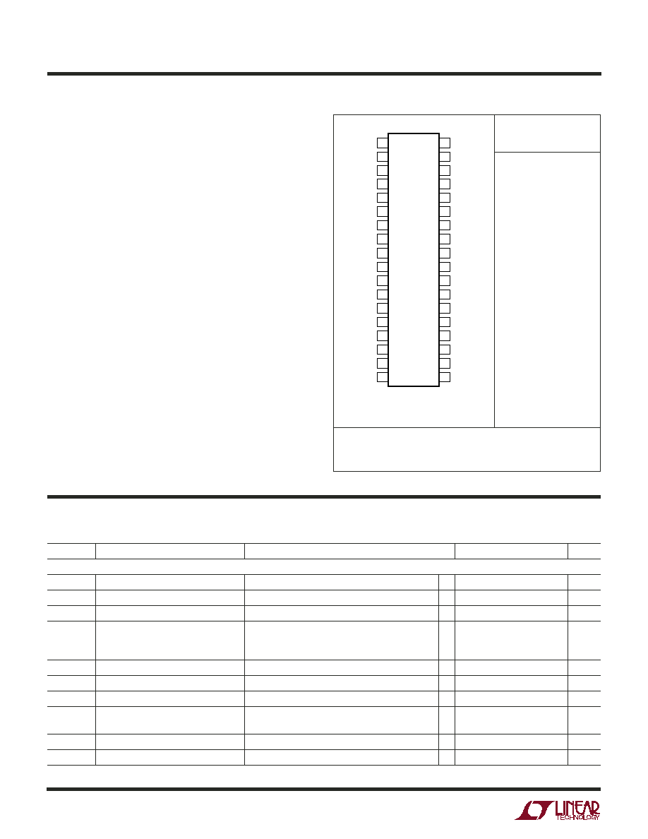
TOP VIEW
G PACKAGE
36-LEAD PLASTIC SSOP
36
35
34
33
32
31
30
29
28
27
26
25
24
23
22
21
20
19
RUN/SS
SENSE1
+
SENSE1
EAIN
PLLFLTR
PLLIN
FCB
I
TH
SGND
V
DIFFOUT
V
OS
V
OS
+
SENSE2
SENSE2
+
ATTENOUT
NO_CPU
VID0
VID1
PGOOD
TG1
SW1
BOOST1
V
IN
BG1
EXTV
CC
INTV
CC
PGND
BG2
BOOST2
SW2
TG2
ATTENIN
V
BIAS
VID4
VID3
VID2
SYMBOL
PARAMETER
CONDITIONS
MIN
TYP
MAX
UNITS
Main Control Loop
V
EAIN
Regulated Feedback Voltage
I
TH
Voltage = 1.2V; Measured at V
EAIN
(Note 4)
0.594
0.600
0.606
V
V
SENSEMAX
Maximum Current Sense Threshold
62
75
88
mV
I
INEAIN
Feedback Current
(Note 4)
5
50
nA
V
LOADREG
Output Voltage Load Regulation
(Note 4)
Measured in Servo Loop,
I
TH
Voltage: 1.2V to 0.7V
0.1
0.5
%
Measured in Servo Loop,
I
TH
Voltage: 1.2V to 2V
0.1
0.5
%
V
REFLNREG
Reference Voltage Line Regulation
V
IN
= 3.6V to 30V (Note 4)
0.002
0.02
%/V
V
FCB
Forced Continuous Threshold
0.57
0.6
0.63
V
I
FCB
Forced Continuous Current
0.17
1
µA
V
BINHIBIT
Burst Inhibit (Constant Frequency)
Measured at FCB pin
4.3
4.8
V
Threshold
V
OVL
Output Overvoltage Threshold
Measured at V
EAIN
0.64
0.66
0.68
V
UVLO
Undervoltage Lockout
V
IN
Ramping Down
3
3.33
4
V
Consult LTC Marketing for parts specified with wider operating temperature ranges.
Order Options Tape and Reel: Add #TR
Lead Free: Add #PBF Lead Free Tape and Reel: Add #TRPBF
Lead Free Part Marking:
http://www.linear.com/leadfree/
3
LTC3819
3819f
ELECTRICAL CHARACTERISTICS
The
denotes the specifications which apply over the full operating
temperature range, otherwise specifications are at T
A
= 25
°C. V
IN
= 15V, V
BIAS
= 5V, V
RUN/SS
= 5V unless otherwise noted.
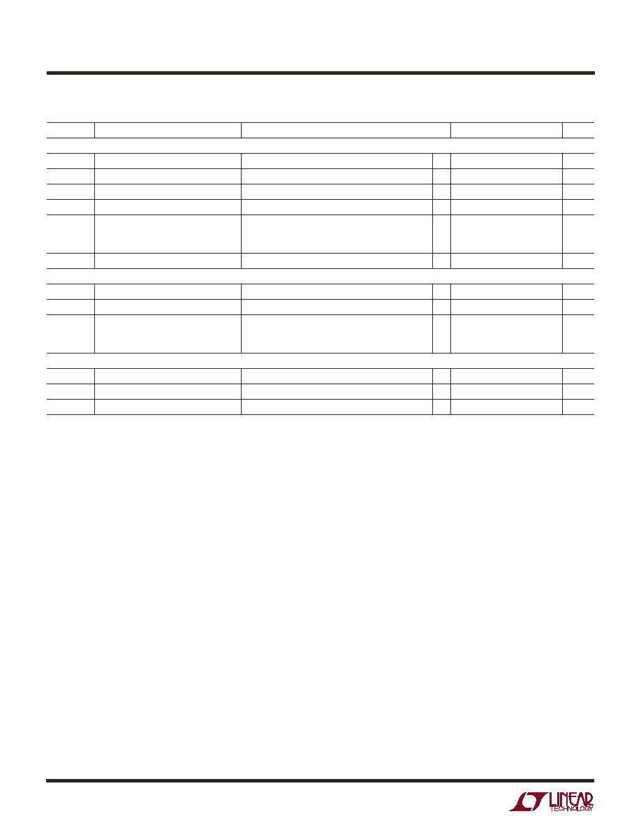
SYMBOL
PARAMETER
CONDITIONS
MIN
TYP
MAX
UNITS
g
m
Transconductance Amplifier g
m
I
TH
= 1.2V, Sink/Source 5
µA (Note 4)
3
mmho
g
mOL
Transconductance Amplifier Gain
I
TH
= 1.2V, (g
m
·
Z
L
; No Ext Load) (Note 4)
1.5
V/mV
I
Q
Input DC Supply Current
(Note 5)
Normal Mode
1.2
mA
Shutdown
V
RUN/SS
= 0V
20
40
µA
I
RUN/SS
Soft-Start Charge Current
V
RUN/SS
= 1.9V
0.5
1.2
µA
V
RUN/SS
RUN/SS Pin ON Threshold
V
RUN/SS
Rising
1.0
1.5
1.9
V
V
RUN/SSLO
RUN/SS Pin Latchoff Arming
V
RUN/SS
Rising from 3V
4.1
4.5
V
I
SCL
RUN/SS Discharge Current
Soft Short Condition V
EAIN
= 0.5V, V
RUN/SS
= 4.5V
0.5
2
4
µA
I
SDLHO
Shutdown Latch Disable Current
V
EAIN
= 0.5V
1.6
5
µA
I
SENSE
Total Sense Pins Source Current
Each Channel: V
SENSE1
, 2
= V
SENSE1
+
, 2
+ = 0V
85
60
µA
DF
MAX
Maximum Duty Factor
In Dropout
98
99.5
%
Top Gate Transition Time:
(Note 6)
TG1, 2 t
r
Rise Time
C
LOAD
= 3300pF
30
90
ns
TG1, 2 t
f
Fall Time
C
LOAD
= 3300pF
40
90
ns
Bottom Gate Transition Time:
(Note 6)
BG1, 2 t
r
Rise Time
C
LOAD
= 3300pF
30
90
ns
BG1, 2 t
f
Fall Time
C
LOAD
= 3300pF
20
90
ns
TG/BG t
1D
Top Gate Off to Bottom Gate On Delay
C
LOAD
= 3300pF Each Driver (Note 6)
90
ns
Synchronous Switch-On Delay Time
BG/TG t
2D
Bottom Gate Off to Top Gate On Delay
C
LOAD
= 3300pF Each Driver (Note 6)
90
ns
Top Switch-On Delay Time
t
ON(MIN)
Minimum On-Time
Tested with a Square Wave (Note 7)
180
ns
Internal V
CC
Regulator
V
INTVCC
Internal V
CC
Voltage
6V < V
IN
< 30V, V
EXTVCC
= 4V
4.8
5.0
5.2
V
V
LDO
INT
INTV
CC
Load Regulation
I
CC
= 0 to 20mA, V
EXTVCC
= 4V
0.2
1.0
%
V
LDO
EXT
EXTV
CC
Voltage Drop
I
CC
= 20mA, V
EXTVCC
= 5V
80
160
mV
V
EXTVCC
EXTV
CC
Switchover Voltage
I
CC
= 20mA, EXTV
CC
Ramping Positive
4.5
4.7
V
V
LDOHYS
EXTV
CC
Switchover Hysteresis
I
CC
= 20mA, EXTV
CC
Ramping Negative
0.2
V
VID Parameters
V
BIAS
Operating Supply Voltage Range
2.7
5.5
V
R
ATTEN
Resistance Between ATTENIN
5
k
and ATTENOUT Pins
ATTEN
ERR
Resistive Divider Error
0.35
0.25
%
R
PULLUP
VID0 to VID4 Pull-Up Resistance
(Note 8)
40
k
VID
THLOW
VID0 to VID4 Logic Threshold Low
0.4
V
VID
THHIGH
VID0 to VID4 Logic Threshold High
1.6
V
VID
LEAK
VID0 to VID4 Leakage
V
BIAS
< VID0VID4 < 7V
±1
µA
V
NO_CPU
NO_CPU Maximum Output Voltage
I
NO_CPU
= 2mA
0.4
V
4
LTC3819
3819f
ELECTRICAL CHARACTERISTICS
The
denotes the specifications which apply over the full operating
temperature range, otherwise specifications are at T
A
= 25
°C. V
IN
= 15V, V
BIAS
= 5V, V
RUN/SS
= 5V unless otherwise noted.
Note 5: Dynamic supply current is higher due to the gate charge being
delivered at the switching frequency. See Applications Information.
Note 6: Rise and fall times are measured using 10% and 90% levels. Delay
times are measured using 50% levels.
Note 7: The minimum on-time condition corresponds to the on inductor
peak-to-peak ripple current
40% I
MAX
(see Minimum On-Time
Considerations in the Applications Information section).
Note 8: Each built-in pull-up resistor attached to the VID inputs also has a
series diode to allow input voltages higher than the VIDV
CC
supply without
damage or clamping (see the Applications Information section).
Note 1: Absolute Maximum Ratings are those values beyond which the
life of a device may be impaired.
Note 2: The LTC3819EG is guaranteed to meet performance specifications
from 0
°C to 70°C. Specifications over the 40°C to 85°C operating
temperature range are assured by design, characterization and correlation
with statistical process controls.
Note 3: T
J
is calculated from the ambient temperature T
A
and power
dissipation P
D
according to the following formula:
LTC3819EG: T
J
= T
A
+ (P
D
· 85
°C/W)
Note 4: The LTC3819 is tested in a feedback loop that servos V
ITH
to a
specified voltage and measures the resultant V
EAIN
.
SYMBOL
PARAMETER
CONDITIONS
MIN
TYP
MAX
UNITS
Oscillator and Phase-Locked Loop
f
NOM
Nominal Frequency
V
PLLFLTR
= 1.2V
190
220
250
kHz
f
LOW
Lowest Frequency
V
PLLFLTR
= 0V
120
140
160
kHz
f
HIGH
Highest Frequency
V
PLLFLTR
2.4V
280
310
360
kHz
R
PLLIN
PLLIN
Input Resistance
50
k
I
PLLFLTR
Phase Detector Output Current
Sinking Capability
f
PLLIN
< f
OSC
15
µA
Sourcing Capability
f
PLLIN
> f
OSC
15
µA
R
RELPHS
Controller 2-Controller 1 Phase
180
Deg
PGOOD Output
V
PGL
PGOOD Voltage Low
I
PGOOD
= 2mA
0.1
0.3
V
I
PGOOD
PGOOD Leakage Current
V
PGOOD
= 5V
±1
µA
V
PG
PGOOD Trip Level, Either Controller
V
EAIN
with Respect to Set Output Voltage
V
EAIN
Ramping Negative
8
10
12
%
V
EAIN
Ramping Positive
8
10
12
%
Differential Amplifier/Op Amp Gain Block
A
DA
Differential Amplifier Gain
V
AMPMD
= 0V
0.995
1
1.005
V/V
CMRR
DA
Common Mode Rejection Ratio
0V < V
CM
< 5V; V
AMPMD
= 0V
46
55
dB
R
IN
Input Resistance
Measured at V
OS
+ Input; V
AMPMD
= 0V
80
k
5
LTC3819
3819f
TYPICAL PERFOR A CE CHARACTERISTICS
U
W
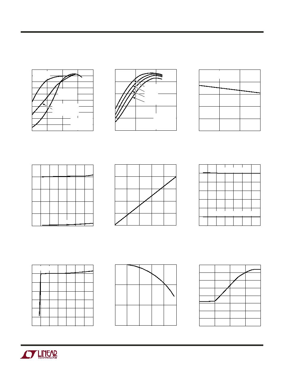
Supply Current vs Input Voltage
and Mode
EXTV
CC
Voltage Drop
INTV
CC
and EXTV
CC
Switch
Voltage vs Temperature
INPUT VOLTAGE (V)
0
5
0
SUPPLY CURRENT (
µ
A)
400
1000
10
20
25
3819 G04
200
800
600
15
30
35
ON
SHUTDOWN
TEMPERATURE (
°C)
50
INTV
CC
AND EXTV
CC
SWITCH VOLTAGE (V)
4.95
5.00
5.05
25
75
3819 G06
4.90
4.85
25
0
50
100
125
4.80
4.70
4.75
INTV
CC
VOLTAGE
EXTV
CC
SWITCHOVER THRESHOLD
Maximum Current Sense Threshold
vs Percent of Nominal Output
Voltage (Foldback)
Internal 5V LDO Line Reg
Maximum Current Sense Threshold
vs Duty Factor
INPUT VOLTAGE (V)
0
4.8
4.9
5.1
15
25
3819 G07
4.7
4.6
5
10
20
30
35
4.5
4.4
5.0
INTV
CC
VOLTAGE (V)
I
LOAD
= 1mA
DUTY FACTOR (%)
0
0
V
SENSE
(mV)
25
50
75
20
40
60
80
3819 G08
100
PERCENT OF NOMINAL OUTPUT VOLTAGE (%)
0
V
SENSE
(mV)
40
50
60
100
3819 G09
30
20
0
25
50
75
10
80
70
Efficiency vs Load Current
(3 Operating Modes) (Figure 12)
LOAD CURRENT (A)
0
EFFICIENCY (%)
10
30
40
50
100
70
0.01
0.1
1
3819 G01
20
80
90
60
100
10
FORCED
CONTINUOUS
MODE
Burst Mode
OPERATION
V
IN
= 5V
V
OUT
= 1.4125V
FREQ = 200kHz
CONSTANT
FREQUENCY
(BURST DISABLED)
Efficiency vs Load Current
(Figure 12)
LOAD CURRENT (A)
0.1
EFFICIENCY (%)
100
80
60
40
20
0
3819 G02
1
10
100
V
OUT
= 1.4125V
V
EXTVCC
= 0V
FREQ = 200kHz
V
FCB
= 0V
V
IN
= 5V
V
IN
= 8V
V
IN
= 12V
V
IN
= 20V
INPUT VOLTAGE (V)
5
EFFICIENCY (%)
70
80
3819 G03
60
50
10
15
20
100
90
I
OUT
= 20A
V
OUT
= 1.4125V
Efficiency vs Input Voltage
(Figure 12)
CURRENT (mA)
0
EXTV
CC
VOLTAGE DROP (mV)
150
200
250
40
3819 G05
100
50
0
10
20
30
50