2927f.indd
LTC2927
1
2927f
RAMP
(3.3V)
2.5V
1.8V
1V/DIV
2927 TA01b
10ms/DIV
RAMP
(3.3V)
2.5V
1.8V
1V/DIV
2927 TA01c
10ms/DIV
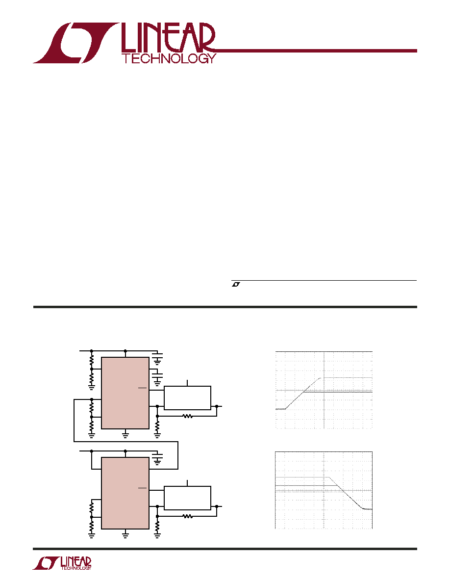
Single Power Supply
Tracking Controller
The LTC
®
2927 provides a simple solution to power supply
tracking and sequencing requirements. By selecting a few
resistors, the supply can be confi gured to ramp-up and
ramp-down with differing ramp rates, voltage offsets, or
time delays relative to other supplies or a master signal.
By forcing current into a feedback node of an independent
supply, the LTC2927 causes the output to track a ramp
signal without inserting any pass element losses. Because
the current is controlled in an open-loop manner, the
LTC2927 does not affect the transient response or stabil-
ity of the supply. The compact solution at point of load
minimizes the trace length of the DC/DC circuit sensitive
FB node. Furthermore, it presents a high impedance when
power-up is complete, effectively removing it from the
DC/DC circuit.
V
CORE
and V
I/O
Supply Tracking
Microprocessor, DSP and FPGA Supplies
Multiple Supply Systems
Point-of-Load Supplies
Flexible Power Supply Tracking
Tracks Both Up and Down
Power Supply Sequencing
Supply Stability is Not Affected
Low Pin Count
Controls Single Supply without Series FETs
Adjustable Ramp Rate
Supply Shutdown Output
Available in 8-Lead ThinSOTTM and 8-Lead
(3mm × 2mm) DFN Packages
138k
100k
ON
RAMP
1.8V
V
CC
V
IN
EARLY V
IN
3.3V
LTC2927
GND
SDO
RUN/SS
FB
IN
DC/DC
FB = 1.235V
OUT
RAMPBUF
TRACK
0.1
µF
16.5k
16.5k
35.7k
13k
ON
RAMP
2.5V
2927 TA01a
V
CC
V
IN
EARLY V
IN
3.3V
LTC2927
GND
SDO
RUN/SS
FB
IN
DC/DC
FB = 0.8V
OUT
RAMPBUF
TRACK
0.1
µF
0.1
µF
887k
887k
412k
412k
, LTC and LT are registered trademarks of Linear Technology Corporation. ThinSOT is a
trademark of Linear Technology Corporation. All other trademarks are the property of their
respective owners. Patents Pending.
APPLICATIO S
U
FEATURES
DESCRIPTIO
U
TYPICAL APPLICATIO
U
Track-Up and Track-Down Waveforms
LTC2927
2
2927f
PACKAGE/ORDER I FOR ATIO
U
U
W
Supply Voltage (V
CC
) ................................. 0.3V to 10V
Input Voltages
ON ......................................................... 0.3V to 10V
TRACK .........................................0.3V to V
CC
+ 0.3V
Output Voltages
FB, SDO ................................................. 0.3V to 10V
RAMP, RAMPBUF ........................0.3V to V
CC
+ 0.3V
(Note 1)
The
denotes the specifi cations which apply over the full operating
temperature range, otherwise specifi cations are at T
A
= 25°C. 2.9V < V
CC
< 5.5V unless otherwise noted (Note 2).
SYMBOL
PARAMETER
CONDITIONS
MIN
TYP
MAX
UNITS
V
CC
Supply Voltage
2.9
5.5
V
I
CC
Supply Current
I
FB
= 0mA, I
TRACK
= 0mA
0.25
0.56
1.2
mA
I
FB
= 1mA, I
TRACK
= 1mA,
I
RAMPBUF
= 1mA
3
3.6
4.2
mA
V
CC(UVLO)
Supply Undervoltage Lockout
V
CC
Rising
2.2
2.5
2.7
V
V
CC(UVHYST)
Supply Undervoltage Lockout Hysteresis
25
mV
V
ON(TH)
ON Pin Threshold Voltage
V
ON
Rising
1.210
1.230
1.250
V
V
ON(HYST)
ON Pin Hysteresis
30
75
150
mV
I
ON
ON Pin Input Current
V
ON
= 1.2V, V
CC
= 5.5V
0
±100
nA
ELECTRICAL CHARACTERISTICS
ABSOLUTE AXI U
RATI GS
W
W
W
U
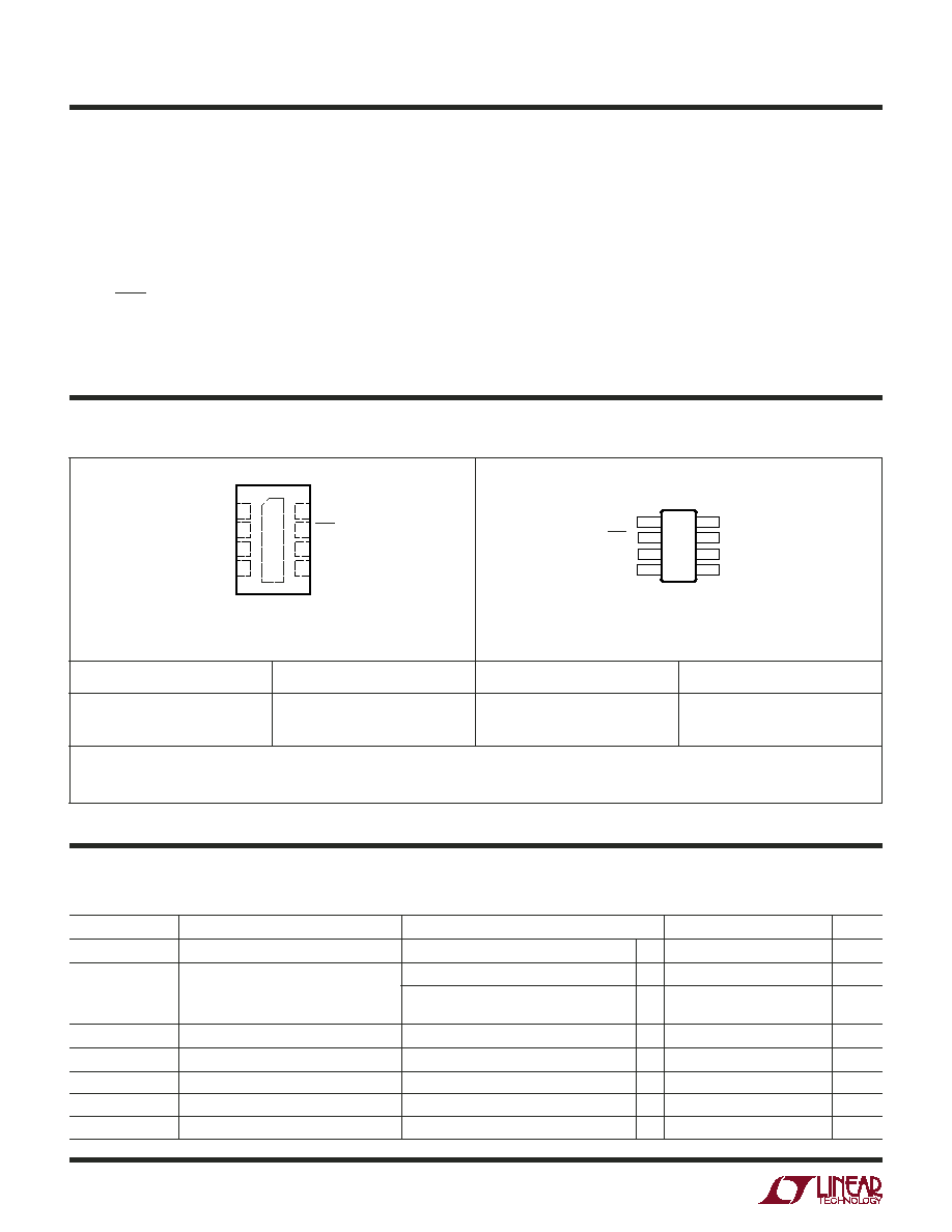
TOP VIEW
DDB PACKAGE
8-LEAD (3mm
× 2mm) PLASTIC DFN
5
6
9
7
8
4
3
2
1
ON
RAMP
RAMPBUF
TRACK
V
CC
SDO
FB
GND
EXPOSED PAD (PIN 9) PCB GND, CONNECTION OPTIONAL
T
JMAX
= 125°C,
JA
= 76°C/W
V
CC
1
SDO 2
FB 3
GND 4
8 ON
7 RAMP
6 RAMPBUF
5 TRACK
TOP VIEW
TS8 PACKAGE
8-LEAD PLASTIC TSOT-23
T
JMAX
= 125°C,
JA
= 250°C/W
ORDER PART NUMBER
DDB PART MARKING*
ORDER PART NUMBER
TS8 PART MARKING*
LTC2927CDDB
LTC2927IDDB
LBQH
LBQH
LTC2927CTS8
LTC2927ITS8
LTBQJ
LTBQJ
Order Options Tape and Reel: Add #TR
Lead Free: Add #PBF Lead Free Tape and Reel: Add #TRPBF
Lead Free Part Marking:
http://www.linear.com/leadfree/
Consult LTC Marketing for parts specifi ed with wider operating temperature ranges. *The temperature grade is identifi ed by a label on the shipping container.
Average Current
TRACK
.................................................................5mA
FB
........................................................................5mA
RAMPBUF
............................................................5mA
Operating Temperature Range
LTC2927C ................................................ 0°C to 70°C
LTC2927I ............................................. 40°C to 85°C
Storage Temperature Range ................... 65°C to 150°C
Lead Temperature (Soldering, 10 sec) .................. 300°C
LTC2927
3
2927f
TEMPERATURE (
°C)
50
770
V
TRACK
(mV)
780
790
800
810
820
25
0
25
50
2927 G03
75
100
V
CC
(V)
4.45
I
CC
(mA)
4.50
4.55
4.60
4.65
4.70
2927 G02
2.5
3.0
3.5
4.0
4.5
6.0
5.5
5.0
I
TRACK
= I
FB
= 1mA
I
RAMBUF
= 2mA
V
CC
(V)
2.5
500
I
CC
(
µ
A)
550
600
650
700
750
3.0
3.5
4.0
4.5
2927 G01
6.0
5.5
5.0
I
TRACK
= I
FB
= 0mA
I
RAMBUF
= 0mA
I
CC
vs V
CC
I
CC
vs V
CC
V
TRACK
vs Temperature
The
denotes the specifi cations which apply over the full operating
temperature range, otherwise specifi cations are at T
A
= 25°C. 2.9V < V
CC
< 5.5V unless otherwise noted (Note 3).
Note 1: Absolute Maximum Ratings are those values beyond which the life
of a device may be impaired.
Note 2: All currents into the device pins are positive; all currents out of
device pins are negative. All voltages are referenced to ground unless
otherwise specifi ed.
SYMBOL
PARAMETER
CONDITIONS
MIN
TYP
MAX
UNITS
I
RAMP
RAMP Pin Input Current
0V < V
RAMP
< V
CC
, Ramp On
9
10
11
µA
0V < V
RAMP
< V
CC
, Ramp Off
9
10
11
µA
V
RAMPBUF(OL)
RAMPBUF Output Low Voltage
I
RAMPBUF
= 1mA
20
100
mV
V
RAMPBUF(OH)
RAMPBUF Output High Voltage,
V
RAMPBUF(OH)
= V
CC
V
RAMPBUF
I
RAMPBUF
= 1mA
45
150
mV
V
OS
Ramp Buffer Offset,
V
OS
= V
RAMPBUF
V
RAMP
V
RAMP
= V
CC
/2, I
RAMPBUF
= 0mA
30
0
30
mV
I
ERROR(%)
I
FB
to I
TRACK
Current Mismatch
I
ERROR(%)
= (I
FB
I
TRACK
)/I
TRACK
I
TRACK
= 10µA
0
±5
%
I
TRACK
= 1mA
0
±5
%
V
TRACK
TRACK Pin Voltage
I
TRACK
= 10µA
0.77
0.800
0.82
V
I
TRACK
= 1mA
0.77
0.800
0.82
V
I
FB(LEAK)
FB Pin Leakage Current
V
FB
= 2V, V
CC
= 5.5V
±1
±100
nA
V
FB(CLAMP)
FB Pin Clamp Voltage
1µA < I
FB
< 1mA
1.5
2
2.3
V
V
SDO(OL)
SDO Output Low Voltage
I
SDO
= 1mA, V
CC
= 2.3V
0.1
0.4
V
ELECTRICAL CHARACTERISTICS
TYPICAL PERFOR A CE CHARACTERISTICS
U
W
LTC2927
4
2927f
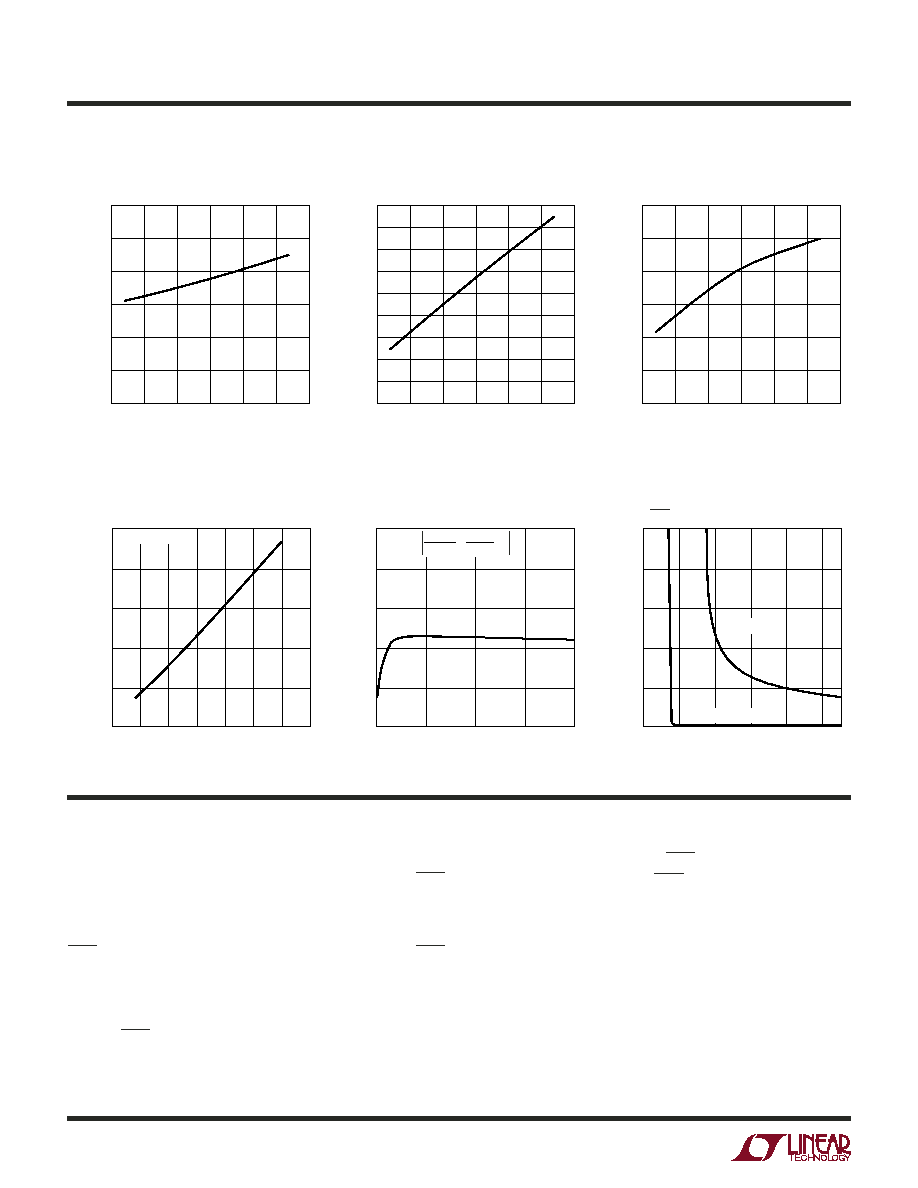
V
CC
(V)
0
0.0
V
SDO(OL)
(V)
0.2
0.4
0.6
0.8
1.0
1
2
3
4
2927 G09
5
I
SDO
= 5mA
I
SDO
= 10
µA
2.5
3.0
3.5
4.0
4.5
6.0
5.5
5.0
V
CC
(V)
10
I
TRACK
(mA)
20
30
40
50
60
2927 G07
V
TRACK
= 0V
I
TRACK
(mA)
1
0
ERROR (%)
1
2
3
4
5
2
3
4
2927 G08
5
ERROR =
·
V
TRACK
0.8V
1
I
FB
I
TRACK
Tracking Cell Error vs I
TRACK
V
SDO(OL)
vs V
CC
V
CC
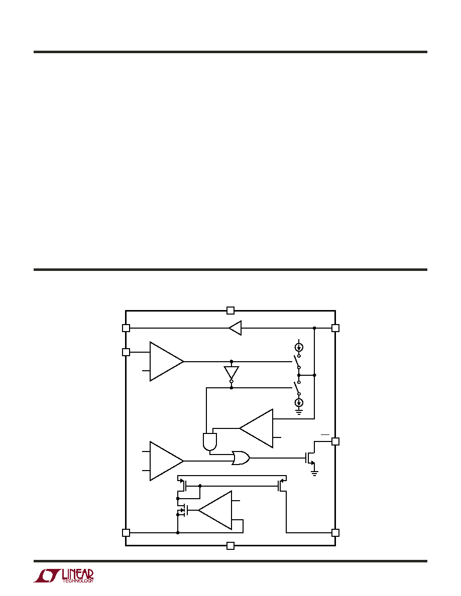
(Pin 1/Pin 8): Supply Voltage Input. Operating range
is from 2.9V to 5.5V. An undervoltage lockout asserts SDO
until V
CC
> 2.5V. V
CC
should be bypassed to GND with a
0.1µF capacitor.
SDO (Pin 2/Pin 7): Slave Supply Shutdown Output. SDO
is an open-drain output that holds the shutdown (RUN/SS)
pin of the slave supply low until the V
CC
pin is pulled above
2.5V, the ON pin is pulled above 1.23V, and RAMP is above
200mV. SDO is pulled low again when RAMP < 200mV and
ON < 1.23V. If the slave supply is capable of operating with
an input supply that is lower than the LTC2927's minimum
operating voltage of 2.9V, the SDO pin can be used to hold
off the slave supply. Tie the SDO pin to GND if unused.
FB (Pin 3/Pin 6): Feedback Control Output. FB pulls up on
the feedback node of the slave supply. Tracking is achieved
by mirroring the current from TRACK into FB. A resistive
divider connecting RAMPBUF and TRACK will force the
output voltage of the slave supply to track RAMP. To prevent
damage to the slave supply, the FB pin will not force the
slave's feedback node above 2.3V. In addition, the LTC2927
will not actively sink current from this node, even when it
is unpowered.
TSOT/DFN Packages
MAX I
TRACK
vs V
CC
TYPICAL PERFOR A CE CHARACTERISTICS
U
W
PI FU CTIO S
U
U
U
TEMPERATURE (
°C)
50
10
18
16
14
12
V
RAMPBUF(OL)
(mV)
20
22
24
26
28
25
0
25
50
2927 G05
75
100
TEMPERATURE (
°C)
50
1.210
1.215
V
ON(TH)
(V)
1.220
1.225
1.230
1.235
1.240
25
0
25
50
2927 G04
75
100
TEMPERATURE (
°C)
50
40
45
V
RAMPBUF(OH)
(mV)
50
55
60
65
70
25
0
25
50
2927 G06
75
100
V
RAMPBUF(OL)
vs Temperature
V
RAMPBUF(OH)
vs Temperature
V
ON(TH)
vs Temperature
LTC2927
5
2927f
0.8V
+
0.2V
10
µA
10
µA
+
5
RAMPBUF
5
RAMP
2927 BD
5
V
CC
5
GND
5
SDO
5
FB
5
ON
5
TRACK
1.23V
+
V
CC
2.5V
+
V
CC
UVLO
V
CC
1x
FU CTIO AL BLOCK DIAGRA
U
U
W
TSOT/DFN Packages
PI FU CTIO S
U
U
U
GND (Pin 4/Pin 5): Device Ground.
TRACK (Pin 5/Pin 4): Tracking Control Input. A resistive
voltage divider between RAMPBUF and TRACK determines
the tracking profi le of the slave supply. TRACK servos to
0.8V, and the current supplied at TRACK is mirrored at FB.
The TRACK pin is capable of supplying at least 1mA when
V
CC
= 2.9V. Under short circuit conditions, the TRACK pin
is capable of supplying up to 70mA. Do not connect to GND
for extended periods. Limit the capacitance at the TRACK
pin to less than 25pF.
RAMPBUF (Pin 6/Pin 3): Ramp Buffer Output. Provides a
low impedance buffered version of the signal on the RAMP
pin. This buffered output drives the resistive voltage divider
that connects to the TRACK pin. Limit the capacitance at
the RAMPBUF pin to less than 100pF. Float RAMPBUF if
unused.
RAMP (Pin 7/Pin 2): Ramp Buffer Input. The RAMP pin is
the input to the voltage buffer whose output drives a resis-
tive voltage divider connected to the TRACK pin. Connect
this input to a capacitor to set the ramp voltage generated
from internal 10µA pull-up or pull-down currents. RAMP
can also be connected to an external ramping signal for
tracking. Ground RAMP if unused.
ON (Pin 8/Pin 1): On Control Input. The voltage level of the
ON pin relative to its 1.23V threshold (with 75mV hysteresis)
controls the tracking direction of the LTC2927. An active
high causes a 10µA pull-up current to fl ow at the RAMP
pin, which charges an external capacitor. An active low at
the ON pin causes a 10µA pull-down current at the RAMP
pin to discharge the external capacitor relative to GND.
Exposed Pad (NA/Pin 9): Exposed pad may be left open or
connected to device ground.