Äîêóìåíòàöèÿ è îïèñàíèÿ www.docs.chipfind.ru
LTC2924
1
2924f
Fully Sequence Four Supplies
Six with Minimal External Circuitry
Cascadable for Additional Supplies
Power Off in Reverse Order or Simultaneously
Charge Pump Drives External MOSFETs
Drives Power Supply Shutdown Pins with No
External Pull-Up Resistors
Sequence and Monitor Two or More Supplies
10µA Output Current Allows Soft-Starting of Supplies
Done Indicator for Both Power On and Power Off
Adjustable Time Delay Between Power Supplies
Power Good Timer
Power Supply Voltage Monitoring and Power
Sequence Error Detection and Reporting
Available in a 16-Lead Narrow SSOP Package
Quad Power Supply
Sequencer
Sequenced Power Supplies for ASICs with Multiple
I/O and Core Voltages
Latch-Up Prevention in Systems with Multiple Power
Supplies
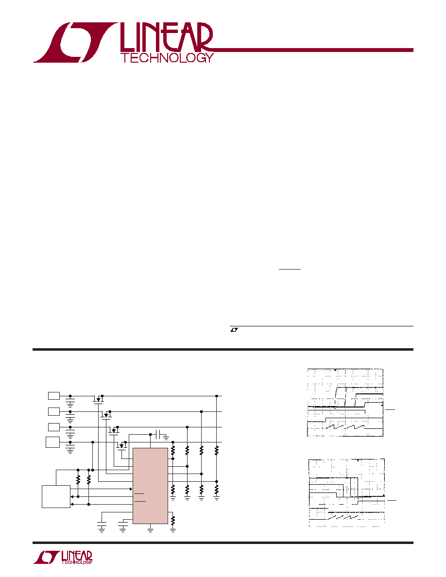
The LTC
®
2924 is a power supply sequencer designed for
use with external N-channel MOSFETs or power supplies
with shutdown pins. Four power supplies can be fully
sequenced by a single LTC2924 and up to five supplies can
be sequenced to a sixth master supply. The LTC2924
requires a minimum of external components, using only
two feedback resistors per sequenced power supply and
a single resistor to set hysteresis.
An internally regulated charge pump provides gate drive
voltages for external logic and sub-logic-level MOSFETs.
Adding a single capacitor enables an adjustable time delay
between power supplies during both Power On and Power
Off sequencing. A second capacitor can be added to enable
a power good timer for detecting the failure of any power
supply to turn on within the selected time. Errors in power
supply sequencing and the control input are detected and
reported at the FAULT output. The LTC2924 features pre-
cision input comparators which can provide 1% accuracy
in monitoring power supply voltages.
Multiple LTC2924s may be easily cascaded to sequence a
virtually unlimited number of power supplies.
FEATURES
DESCRIPTIO
U
APPLICATIO S
U
TYPICAL APPLICATIO
U
OUT1
OUT2
OUT3
OUT4
ON
DONE
FAULT
TMR
PGT
IN1
IN2
IN3
IN4
HYS/CFG
LTC2924
V
CC
GND
150nF
2924 TA02a
SYSTEM
CONTROLLER
150nF
0.1µF
0.1µF
0.1µF
0.1µF
11.8k
52.3k
0.1µF
Q4
Q3
Q2
Q1
45.3k
6.04k
1.62k
7.68k
1.69k
Q1-Q4: IRL3714S
ALL RESISTORS 1%
3.09k
V
ON
= 0.93V
V
OFF
= 0.91V
V
ON
= 2.79V
V
OFF
= 2.73V
V
ON
= 4.21V
V
OFF
= 3.76V
V
ON
= 3.32V
V
OFF
= 2.80V
49.9k
10k
5V
EARLY
10k
5V
3V
1V
Series MOSFET Power Supply Sequencer
2V/DIV
5V
3.3V
1V
DONE
ON
TMR
10V/DIV
2V/DIV
2V/DIV
25ms/DIV
2924 TA02b
2V/DIV
5V
3.3V
1V
DONE
ON
TMR
10V/DIV
2V/DIV
2V/DIV
25ms/DIV
2924 TA02c
Power-Down Sequence
Power-Up Sequence
, LTC and LT are registered trademarks of Linear Technology Corporation.
All other trademarks are the property of their respective owners.
LTC2924
2
2924f
Supply Voltage (V
CC
) ............................... 0.3V to 6.5V
Input Voltages
ON, IN1-IN4 ............................... 0.3V to V
CC
+ 0.3V
PGT, TMR, HYS/CFG ................. 0.3V to V
CC
+ 0.3V
Open-Drain Output Voltages
FAULT, DONE ............................. 0.3V to V
CC
+ 0.3V
Output Voltages
(OUT1-OUT4) (Note 5) ............... 0.3V to V
CC
+ 4.5V
Operating Temperature Range
LTC2924C ............................................... 0°C to 70°C
LTC2924I ............................................ 40°C to 85°C
Storage Temperature Range ................ 65°C to 150°C
Lead Temperature (Soldering, 10 sec)................. 300°C
ORDER PART
NUMBER
(Note 1)
ABSOLUTE AXI U RATI GS
W
W
W
U
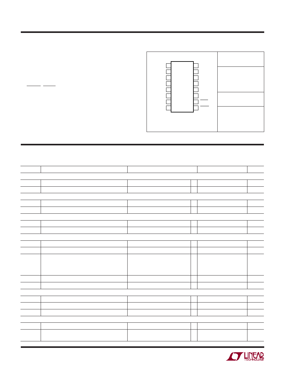
PACKAGE/ORDER I FOR ATIO
U
U
W
Consult LTC Marketing for parts specified with wider operating temperature ranges.
LTC2924CGN
LTC2924IGN
T
JMAX
= 125°C,
JA
= 130°C/W
The
denotes the specifications which apply over the full operating
temperature range, otherwise specifications are at T
A
= 25°C. V
CC
= 3V to 6V, unless otherwise noted.
ELECTRICAL CHARACTERISTICS
GN PACKAGE
16-LEAD PLASTIC SSOP
1
2
3
4
5
6
7
8
TOP VIEW
16
15
14
13
12
11
10
9
IN1
IN2
IN3
IN4
OUT1
OUT2
OUT3
OUT4
ON
HYS/CFG
TMR
GND
PGT
V
CC
DONE
FAULT
GN PART
MARKING
2924
2924I
SYMBOL
PARAMETER
CONDITIONS
MIN
TYP
MAX
UNITS
Supply
V
CC
Input Supply Range
3
6
V
I
CC
Input Supply Current
1.5
3
mA
ON Threshold
V
ON(TH)
ON, Low to High Threshold
0.6000
0.6060
0.6121
V
V
OFF(TH)
ON, High to Low Threshold
0.6014
0.6074
0.6135
V
IN1-IN4 Threshold
V
ON(TH)
IN1-IN4 Low to High Threshold
0.6020
0.6081
0.6142
V
V
OFF(TH)
IN1-IN4 High to Low Threshold
0.6026
0.6087
0.6148
V
ON, IN1-IN4 Characteristics
V
FAULT
ON, IN1-IN4 High Speed Low Fault Threshold
0.33
0.4
0.48
V
I
ON(HYS)
ON, IN1-IN4 Hysteresis Current Range
V
ON
V
ON(TH)
(Note 2)
0.5
50
µA
I
ON(ERROR)
ON, IN1-IN4 Hysteresis Current Error
1 (I
ON(HYS)
/(0.5/R
HYS
)),
V
ON(TH)
= 1V
0.5µA I
ON
< 25µA
±22
%
25µA I
ON
50µA
±10
%
I
LEAK
ON, IN1-IN4 Leakage (Below Threshold)
V
ON(TH)
= 0.5V
2
±100
nA
V
ON(HYS)
ON, IN1-IN4 Minimum Hysteresis Voltage
I
HYS
· R
HYS
4
mV
OUT1-OUT4 Characteristics
V
OUT(EN)
OUT1-OUT4 Gate Drive Voltage
I
OUT
n
= 0
V
CC
+ 4.5
V
CC
+ 6
V
I
OUT(EN)
OUT1-OUT4 On Current
OUT
n On, V
OUT
= (V
CC
+ 4V)
8.6
10
11.2
µA
R
OUT(OFF)
OUT1-OUT4 Off Resistance to GND
OUT
n Off, I
OUT
= 2mA
240
HYS Characteristics
R
HYS
HYS Current Programming Resistor Range
(Notes 2, 3)
10k
1M
V
HYS
HYS Programming Voltage
R
HYS
Tied to GND
0.5
V
R
HYS
Tied to V
CC
V
CC
0.5
V
LTC2924
3
2924f
The
denotes the specifications which apply over the full operating
temperature range, otherwise specifications are at T
A
= 25°C. V
CC
= 3V to 6V, unless otherwise noted.
ELECTRICAL CHARACTERISTICS
Note 1: Absolute Maximum Ratings are those values beyond which the life
of a device may be impaired.
Note 2: Hysteresis current must be 500nA minimum. Hysteresis current
may exceed 50µA, but accuracy is not guaranteed.
Note 3: HYS/CFG pin must be pulled to GND or V
CC
with an external
resistor. See Applications Information for details.
Note 4: Determined by design, not production tested. External circuits
pulling down on the FAULT pin must maintain the signal below V
FAULT(LO)
for 1µs.
Note 5: Internal circuits may drive the OUT
n pins higher than the Absolute
Maximum Ratings.
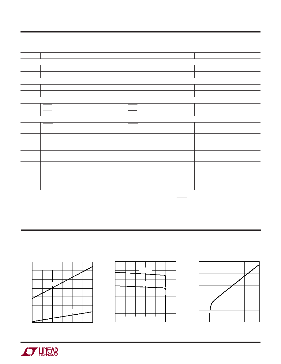
TYPICAL PERFOR A CE CHARACTERISTICS
U
W
I
CC
vs V
CC
V
CC
(V)
3
2.3
2.1
1.9
1.7
1.5
1.3
1.1
0.9
4.5
5.5
2924 G01
3.5
4
5
6
I
CC
(mA)
I
OUT1-4
= 10µA
R
HYS
= 51k
ON HIGH
ON LOW
I
OUT
(µA)
0
14
12
10
8
6
4
2
0
6
10
2924 G02
2
4
8
12
V
OUT
(V)
V
CC
= 6V
ONE OUTPUT DRIVING CURRENT
V
CC
= 3V
V
CC
(V)
2
V
OUT
(V)
9
10
6
2924 G03
8
7
3
4
5
12
11
I
OUT1-4
< 1µA
V
OUT(EN)
vs I
OUT
V
OUT(EN)
vs V
CC
SYMBOL
PARAMETER
CONDITIONS
MIN
TYP
MAX
UNITS
TMR Characteristics
I
TMR
Timer Pin Output Current
Timer On V
TMR
0.9V
4
5
6
µA
V
TH(HI)
Timer High Voltage Threshold
V
CC
= 5V
0.93
1
1.07
V
PGT Characteristics
I
PGT
Power Good Timer Pin Output Current
Power Good Timer On, V
PGT
0.9V
4
5
6
µA
V
PGT
Power Good Timer Fault Detected Voltage Threshold
V
CC
= 5V
0.93
1
1.07
V
DONE Characteristics
R
D(LO)
DONE Pin Pull-Down Resistance to GND
DONE = Low, I = 2mA
100
I
D(HI)
DONE Pin Off Leakage Current
DONE = High
15
µA
FAULT Characteristics
R
FAULT (LO)
FAULT Pin Pull-Down Resistance to GND
FAULT Being Pulled Low Internally,
400
I = 2mA
I
FAULT(HI)
FAULT Pin Off Leakage Current
FAULT High
2
µA
V
FAULT(HI)
Voltage Above Which an Externally Generated
1.6
V
FAULT Condition Will Not be Detected
V
FAULT(LO)
Voltage Below Which an Externally Generated
0.6
V
FAULT Condition Will be Detected
R
F(EXT)
External Pull-Up Resistance
10
k
t
FAULT
Externally Commanded FAULT Below V
FAULT(LO)
1
µs
to OUT1-OUT4 Pull-Down On Delay
t
FAULT(MIN)
Externally Commanded FAULT Minimum Time
(Note 4)
1
µs
Below V
FAULT(LO)
LTC2924
4
2924f
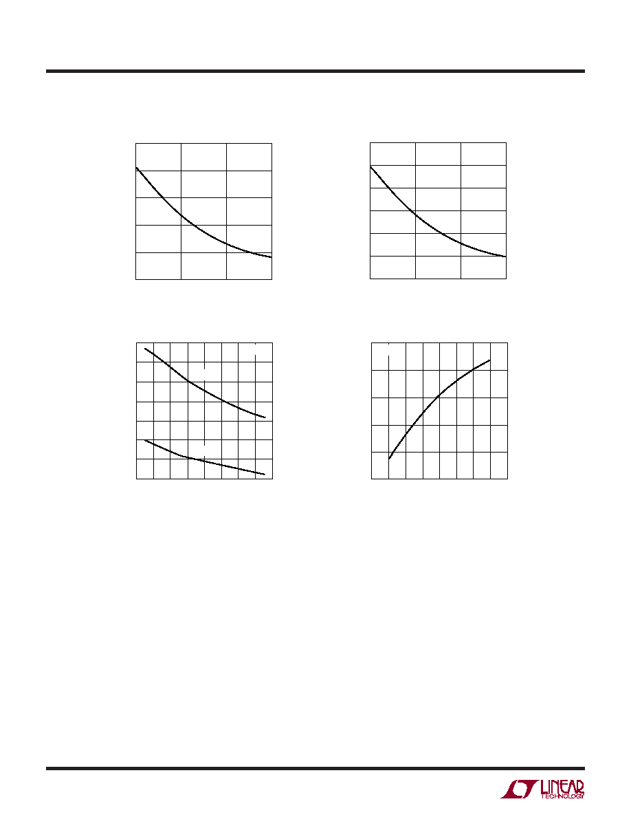
TYPICAL PERFOR A CE CHARACTERISTICS
U
W
R
DONE
vs V
CC
R
FAULT
vs V
CC
OUT
n (Off) I
SAT
vs Temperature
V
CC
(V)
3
R
DONE
AT 2mA (
)
40
45
2924 G04
35
30
4
5
6
55
50
V
CC
(V)
3
R
FAULT
AT 2mA (
)
120
140
2924 G05
100
80
4
5
6
200
180
160
OUT
n (Off) I
SAT
vs V
CC
TEMPERATURE (°C)
60 40
I
SAT
(mA)
30
35
40
60
2924 G06
25
20
20
0
20
40
80
100
15
10
45
V
OUT
= 5V
V
CC
= 6V
V
CC
= 3V
V
CC
(V)
2.5
I
SAT
(mA)
25
30
35
4
5
6.5
2924 G07
20
15
10
3
3.5
4.5
5.5
6
V
OUT
= 5V

LTC2924
5
2924f
IN1-IN4 (Pins 1, 2, 3, 4): Sequenced Power Supply
Monitor. Connect this pin to an external resistive divider
between each sequenced power supply and GND. During
Power On sequencing, 0.61V (typ) at this pin indicates that
the sequenced power supply (enabled with each of the
OUT1-OUT4 pins) has reached the desired Power On
sequence voltage. A hysteresis current (programmed by
the HYS pin) is sourced out of each of the IN1-IN4 pins
after the 0.61V threshold is detected. During the Power Off
sequence, 0.61V at this pin indicates that the sequenced
power supply has reached the desired Power Off voltage.
The hysteresis current is removed after the 0.61V thresh-
old is detected.
OUT1-OUT4 (Pins 5, 6, 7, 8): Sequenced Power Supply
Enable. Connect this pin to the shutdown pin or an external
series N-channel MOSFET for each power supply being
sequenced. (A low at this pin means the sequenced power
supply is commanded to turn off.) When disabled, each
output is connected to GND with a resistance of <240.
When enabled, each output is connected to an internally
generated charge pump supply (nominally V
CC
+ 5V) via
an internal 10µA (typ) current source.
FAULT (Pin 9): Fault Pin. Pull this pin high with an external
10k resistor. The LTC2924 will pull this pin low if a fault
condition is detected (see Applications Information for
details). Pulling this pin low externally causes a simulta-
neous unsequenced Power Off.
DONE (Pin 10): Done Pin. Pull this pin high with an
external 10k resistor. This open-drain output pulls low at
the completion of the Power-On sequence. At the end of
the Power Off sequence, the LTC2924 floats this pin.
V
CC
(Pin 11): Power Supply Input. All internal circuits are
powered from this pin. V
CC
should be connected to a low
noise power supply voltage and should be bypassed with
at least a 0.1µF capacitor to the GND pin in close proximity
to the LTC2924.
PGT (Pin 12): Power Good Timer. The PGT pin sets the
time allowed for a power supply to turn on after being
enabled with the OUT1-OUT4 pins. Connecting a capacitor
between this pin and ground programs a 0.2µs/µF dura-
tion. The PGT pin is reset before each of the OUT1-OUT4
pins are asserted. If the voltage at the PGT pin reaches 1V,
a fault condition is asserted. The PGT pin must be con-
nected directly to ground to disable the power good timer
function.
GND (Pin 13): Ground. All internal circuits are returned to
the GND pin. Connect this pin to the ground of the power
supplies that are being sequenced.
TMR (Pin 14): Timer. This pin sets the time delay between
a supply ready (IN1-IN4) signal and the enabling of the
next power supply in the sequence (OUT1-OUT4). Con-
necting a capacitor between this pin and ground programs
a 0.2µs/µF duration. The TMR pin may be left floating if no
delay is required between supplies being sequenced on or
off. If an internal fault condition occurs, TMR will indicate
so by going to V
CC
until the fault condition is cleared. Do
not connect any other circuits to the TMR pin.
HYS/CFG (Pin 15): Hysteresis Current Setting and Cas-
cade Configuration. Connecting a resistor between this
pin and GND programs a 0.5/R
EXT
(typ) hysteresis current
which is sourced out of each IN and ON pin. When multiple
LTC2924s are cascaded, the HYS/CFG pin is also used to
configure the position of the
first LTC2924. See Applica-
tions Information for details.
ON (Pin 16): On Pin. Commands the LTC2924 to sequence
the power supplies up (Power On sequence) or down
(Power Off sequence). Typically connected to a system
controller. Hysteresis current is applied to this pin when
above 0.61V (typ). This pin has a precision 0.61V thresh-
old and can be used to sense a nonsequenced power
supply's voltage to start the Power On sequence. See
Applications Information for details. For cascading mul-
tiple LTC2924s, see Applications Information for connect-
ing the ON pin.
U
U
U
PI FU CTIO S