Äîêóìåíòàöèÿ è îïèñàíèÿ www.docs.chipfind.ru
1
LTC2601/LTC2611/LTC2621
2601f
16-/14-/12-Bit Rail-to-Rail
DACs in 10-Lead DFN
The LTC
®
2601/LTC2611/LTC2621 are single 16-, 14-
and 12-bit, 2.5V-to-5.5V rail-to-rail voltage output DACs
in a 10-lead DFN package. They have built-in high perfor-
mance output buffers and are guaranteed monotonic.
These parts establish new board-density benchmarks for
16- and 14-bit DACs and advance performance standards
for output drive, and load regulation in single-supply,
voltage-output multiples.
The parts use a simple SPI/MICROWIRE
TM
compatible
3-wire serial interface which can be operated at clock rates
up to 50MHz. Daisy-chain capability, hardware CLR and
asynchronous DAC update (LDAC) pins are included.
The LTC2601/LTC2611/LTC2621 incorporate a power-on
reset circuit. During power-up, the voltage outputs rise
less than 10mV above zero scale; and after power-up, they
stay at zero scale until a valid write and update take place.
s
Smallest Pin-Compatible Single DACs:
LTC2601: 16 Bits
LTC2611: 14 Bits
LTC2621: 12 Bits
s
Guaranteed Monotonic Over Temperature
s
Wide 2.5V to 5.5V Supply Range
s
Low Power Operation: 300
µ
A at 3V
s
Power Down to 1
µ
A, Max
s
High Rail-to-Rail Output Drive (
±
15mA, Min)
s
Double-Buffered Data Latches
s
Asynchronous DAC Update Pin
s
Tiny (3mm
×
3mm) 10-Lead DFN Package
s
Mobile Communications
s
Process Control and Industrial Automation
s
Instrumentation
s
Automatic Test Equipment
Differential Nonlinearity (LTC2601)
, LTC and LT are registered trademarks of Linear Technology Corporation.
MICROWIRE is a trademark of National Semiconductor Corporation.
U.S. patent number 5396245.
APPLICATIO S
U
FEATURES
DESCRIPTIO
U
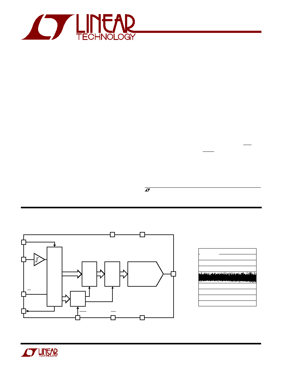
BLOCK DIAGRA
W
7
10
1
DAC
REGISTER
INPUT
REGISTER
32-BIT
SHIFT
REGISTER
12-/14-/16-BIT DAC
V
OUT
CONTROL
DECODE
LOGIC
LDAC
SDO
2
SDI
SCK
5
CS/LD
9
V
CC
6
REF
8
GND
2601 BD
4
CLR
3
CODE
0
16384
32768
49152
65535
DNL (LSB)
2600 G02
1.0
0.8
0.6
0.4
0.2
0
0.2
0.4
0.6
0.8
1.0
V
CC
= 5V
V
REF
= 4.096V
2
LTC2601/LTC2611/LTC2621
2601f
A
U
G
W
A
W
U
W
A
R
BSOLUTE
XI
TI
S
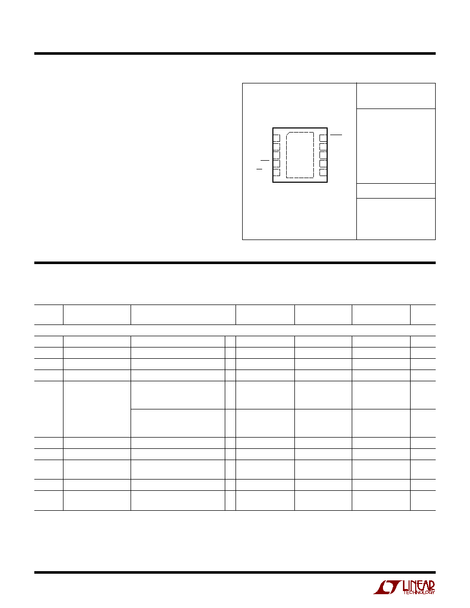
ORDER PART
NUMBER
W
U
U
PACKAGE/ORDER I FOR ATIO
T
JMAX
= 125
°
C,
JA
= 43
°
C/W
EXPOSED PAD (PIN 11) IS GND
MUST BE SOLDERED TO PCB
(Note 1)
Any Pin to GND ........................................... 0.3V to 6V
Any Pin to V
CC
............................................. 6V to 0.3V
Maximum Junction Temperature ......................... 125
°
C
Operating Temperature Range
LTC2601C/LTC2611C/LTC2621C .......... 0
°
C to 70
°
C
LTC2601I/LTC2611I/LTC2621I .......... 40
°
C to 85
°
C
Storage Temperature Range ................ 65
°
C to 125
°
C
Lead Temperature (Soldering, 10 sec)................ 300
°
C
DD PART MARKING
ELECTRICAL C
C
HARA TERISTICS
The
q
denotes specifications which apply over the full operating
temperature range, otherwise specifications are at T
A
= 25
°
C. REF = 4.096V (V
CC
= 5V), REF = 2.048V (V
CC
= 2.5V), V
OUT
unloaded,
unless otherwise noted.
LTC2601CDD
LTC2601IDD
LTC2611CDD
LTC2611IDD
LTC2621CDD
LTC2621IDD
LAGT
LBFQ
LBFS
Consult LTC Marketing for parts specified with wider operating temperature ranges.
TOP VIEW
11
DD PACKAGE
10-LEAD (3mm
×
3mm) PLASTIC DFN
10
9
6
7
8
4
5
3
2
1
LDAC
V
CC
GND
V
OUT
REF
SDO
SDI
SCK
CLR
CS/LD
LTC2621
LTC2611
LTC2601
SYMBOL
PARAMETER
CONDITIONS
MIN
TYP
MAX
MIN
TYP
MAX
MIN
TYP
MAX
UNITS
DC Performance
Resolution
q
12
14
16
Bits
Monotonicity
(Note 2)
q
12
14
16
Bits
DNL
Differential Nonlinearity
(Note 2)
q
±
0.5
±
1
±
1
LSB
INL
Integral Nonlinearity
(Note 2)
q
±
0.8
±
4
±
3
±
16
±
13
±
64
LSB
Load Regulation
V
REF
= V
CC
= 5V, Midscale
I
OUT
= 0mA to 15mA Sourcing
q
0.03 0.125
0.10
0.5
0.45
2
LSB/mA
I
OUT
= 0mA to 15mA Sinking
q
0.04 0.125
0.15
0.5
0.60
2
LSB/mA
V
REF
= V
CC
= 2.5V, Midscale
I
OUT
= 0mA to 7.5mA Sourcing
q
0.06
0.25
0.2
1
0.9
4
LSB/mA
I
OUT
= 0mA to 7.5mA Sinking
q
0.08
0.25
0.3
1
1.2
4
LSB/mA
ZSE
Zero-Scale Error
Code = 0
q
1
9
1
9
1
9
mV
V
OS
Offset Error
(Note 5)
q
±
1.5
±
9
±
1.5
±
9
±
1.5
±
9
mV
V
OS
Temperature
±
5
±
5
±
5
µ
V/
°
C
Coefficient
GE
Gain Error
q
±
0.03
±
0.7
±
0.1
±
0.7
±
0.05
±
0.7
%FSR
Gain Temperature
±
2
±
2
±
2
ppm/
°
C
Coefficient
3
LTC2601/LTC2611/LTC2621
2601f
ELECTRICAL C
C
HARA TERISTICS
The
q
denotes specifications which apply over the full operating
temperature range, otherwise specifications are at T
A
= 25
°
C. REF = 4.096V (V
CC
= 5V), REF = 2.048V (V
CC
= 2.5V), V
OUT
unloaded,
unless otherwise noted.
LTC2601/LTC2611/LTC2621
SYMBOL
PARAMETER
CONDITIONS
MIN
TYP
MAX
UNITS
PSR
Power Supply Rejection
V
CC
= 5V
±
10%
80
dB
V
CC
= 3V
±
10%
q
80
dB
R
OUT
DC Output Impedance
V
REF
= V
CC
= 5V, Midscale; 15mA
I
OUT
15mA
q
0.04
0.15
V
REF
= V
CC
= 2.5V, Midscale; 7.5mA
I
OUT
7.5mA
q
0.05
0.15
I
SC
Short-Circuit Output Current
V
CC
= 5.5V, V
REF
= 5.5V
Code: Zero Scale; Forcing Output to V
CC
q
15
35
60
mA
Code: Full Scale; Forcing Output to GND
q
15
39
60
mA
V
CC
= 2.5V, V
REF
= 2.5V
Code: Zero Scale; Forcing Output to V
CC
q
7.5
20
50
mA
Code: Full Scale; Forcing Output to GND
q
7.5
27
50
mA
Reference Input
Input Voltage Range
q
0
V
CC
V
Resistance
Normal Mode
q
88
124
160
k
Capacitance
15
pF
I
REF
Reference Current, Power Down Mode
DAC Powered Down
q
0.001
1
µ
A
Power Supply
V
CC
Positive Supply Voltage
For Specified Performance
q
2.5
5.5
V
I
CC
Supply Current
V
CC
= 5V (Note 3)
q
0.375
0.55
mA
V
CC
= 3V (Note 3)
q
0.30
0.45
mA
DAC Powered Down (Note 3) V
CC
= 5V
q
0.40
1
µ
A
DAC Powered Down (Note 3) V
CC
= 3V
q
0.10
1
µ
A
Digital I/O
V
IH
Digital Input High Voltage
V
CC
= 2.5V to 5.5V
q
2.4
V
V
CC
= 2.5V to 3.6V
q
2.0
V
V
IL
Digital Input Low Voltage
V
CC
= 4.5V to 5.5V
q
0.8
V
V
CC
= 2.5V to 5.5V
q
0.6
V
V
OH
Digital Output High Voltage
Load Current = 100
µ
A
q
V
CC
0.4
V
V
OL
Digital Output Low Voltage
Load Current = +100
µ
A
q
0.4
V
I
LK
Digital Input Leakage
V
IN
= GND to V
CC
q
±
1
µ
A
C
IN
Digital Input Capacitance
(Note 4)
q
8
pF
4
LTC2601/LTC2611/LTC2621
2601f
TI I G CHARACTERISTICS
U
W
The
q
denotes specifications which apply over the full operating temperature
range, otherwise specifications are at T
A
= 25
°
C. (See Figure 1) (Note 4)
Note 1: Absolute maximum ratings are those values beyond which the life
of a device may be impaired.
Note 2: Linearity and monotonicity are defined from code k
L
to code
2
N
1, where N is the resolution and k
L
is given by k
L
= 0.016(2
N
/V
REF
),
rounded to the nearest whole code. For V
REF
= 4.096V and N = 16, k
L
=
256 and linearity is defined from code 256 to code 65,535.
Note 3: Digital inputs at 0V or V
CC
.
Note 4: Guaranteed by design and not production tested.
Note 5: Inferred from measurement at code K
L
= 0.016(2
N
/V
REF
) and at
full scale.
Note 6: V
CC
= 5V, V
REF
= 4.096V. DAC is stepped 1/4 scale to 3/4 scale
and 3/4 scale to 1/4 scale. Load is 2k in parallel with 200pF to GND.
Note 7: V
CC
= 5V, V
REF
= 4.096V. DAC is stepped
±
1LSB between half
scale and half scale 1. Load is 2k in parallel with 200pF to GND.
ELECTRICAL C
C
HARA TERISTICS
The
q
denotes specifications which apply over the full operating
temperature range, otherwise specifications are at T
A
= 25
°
C. REF = 4.096V (V
CC
= 5V), REF = 2.048V (V
CC
= 2.5V), V
OUT
unloaded,
unless otherwise noted.
LTC2621
LTC2611
LTC2601
SYMBOL
PARAMETER
CONDITIONS
MIN
TYP
MAX
MIN
TYP
MAX
MIN
TYP
MAX
UNITS
AC Performance
t
S
Settling Time (Note 6)
±
0.024% (
±
1LSB at 12 Bits)
7
7
7
µ
s
±
0.006% (
±
1LSB at 14 Bits)
9
9
µ
s
±
0.0015% (
±
1LSB at 16 Bits)
10
µ
s
Settling Time for 1LSB Step
±
0.024% (
±
1LSB at 12 Bits)
2.7
2.7
2.7
µ
s
(Note 7)
±
0.006% (
±
1LSB at 14 Bits)
4.8
4.8
µ
s
±
0.0015% (
±
1LSB at 16 Bits)
5.2
µ
s
Voltage Output Slew Rate
0.80
0.80
0.80
V/
µ
s
Capacitive Load Driving
1000
1000
1000
pF
Glitch Impulse
At Midscale Transition
12
12
12
nV · s
Multiplying Bandwidth
180
180
180
kHz
e
n
Output Voltage Noise Density
At f = 1kHz
120
120
120
nV/
Hz
At f = 10kHz
100
100
100
nV/
Hz
Output Voltage Noise
0.1Hz to 10Hz
15
15
15
µ
V
P-P
LTC2601/LTC2611/LTC2621
SYMBOL
PARAMETER
CONDITIONS
MIN
TYP
MAX
UNITS
V
CC
= 2.5V to 5.5V
t
1
SDI Valid to SCK Setup
q
4
ns
t
2
SDI Valid to SCK Hold
q
4
ns
t
3
SCK High Time
q
9
ns
t
4
SCK Low Time
q
9
ns
t
5
CS/LD Pulse Width
q
10
ns
t
6
LSB SCK High to CS/LD High
q
7
ns
t
7
CS/LD Low to SCK High
q
7
ns
t
8
SDO Propagation Delay from SCK Falling Edge
C
LOAD
= 10pF
V
CC
= 4.5V to 5.5V
q
20
ns
V
CC
= 2.5V to 5.5V
q
45
ns
t
9
CLR Pulse Width
q
20
ns
t
10
CS/LD High to SCK Positive Edge
q
7
ns
t
12
LDAC Pulse Width
q
15
ns
t
13
CS/LD High to LDAC High or Low Transition
q
200
ns
SCK Frequency
50% Duty Cycle
q
50
MHz
5
LTC2601/LTC2611/LTC2621
2601f
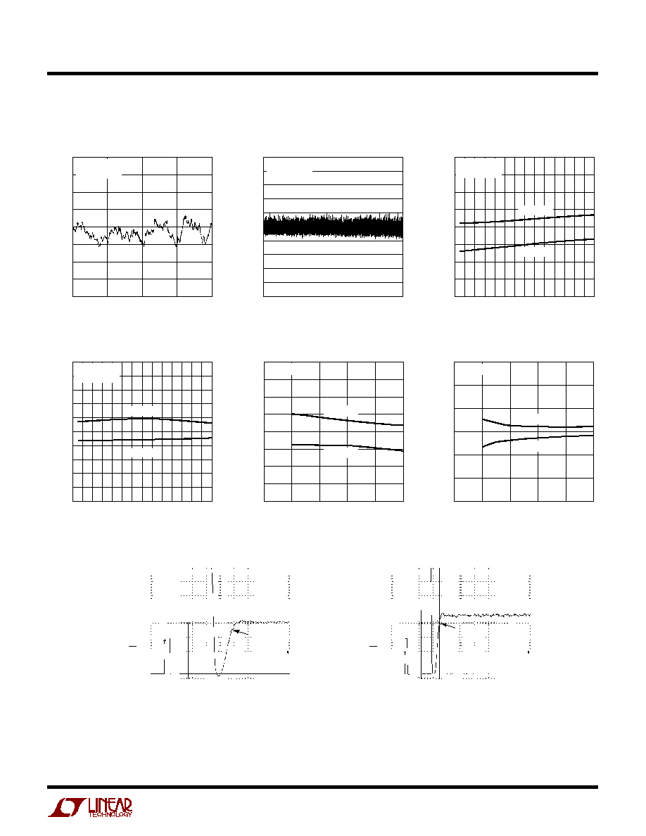
TYPICAL PERFOR A CE CHARACTERISTICS
U
W
Settling to
±
1LSB
Settling of Full-Scale Step
LTC2601
Integral Nonlinearity (INL)
Differential Nonlinearity (DNL)
INL vs Temperature
DNL vs Temperature
INL vs V
REF
DNL vs V
REF
CODE
0
16384
32768
49152
65535
INL (LSB)
2601 G01
32
24
16
8
0
8
16
24
32
V
CC
= 5V
V
REF
= 4.096V
CODE
0
16384
32768
49152
65535
DNL (LSB)
2600 G02
1.0
0.8
0.6
0.4
0.2
0
0.2
0.4
0.6
0.8
1.0
V
CC
= 5V
V
REF
= 4.096V
TEMPERATURE (
°
C)
50
30
10
10
30
50
70
90
INL (LSB)
2601 G03
32
24
16
8
0
8
16
24
32
V
CC
= 5V
V
REF
= 4.096V
INL (POS)
INL (NEG)
TEMPERATURE (
°
C)
50
30
10
10
30
50
70
90
DNL (LSB)
2601 G04
1.0
0.8
0.6
0.4
0.2
0
0.2
0.4
0.6
0.8
1.0
V
CC
= 5V
V
REF
= 4.096V
DNL (POS)
DNL (NEG)
V
REF
(V)
0
1
2
3
4
5
INL (LSB)
2601 G05
32
24
16
8
0
8
16
24
32
V
CC
= 5.5V
INL (POS)
INL (NEG)
V
REF
(V)
0
1
2
3
4
5
DNL (LSB)
2601 G06
1.5
1.0
0.5
0
0.5
1.0
1.5
V
CC
= 5.5V
DNL (POS)
DNL (NEG)
2
µ
s/DIV
2601 G07
V
OUT
100
µ
V/DIV
CS/LD
2V/DIV
V
CC
= 5V, V
REF
= 4.096V
1/4-SCALE TO 3/4-SCALE STEP
R
L
= 2k, C
L
= 200pF
AVERAGE OF 2048 EVENTS
9.7
µ
s
5
µ
s/DIV
2601 G08
V
OUT
100
µ
V/DIV
CS/LD
2V/DIV
SETTLING TO
±
1LSB
V
CC
= 5V, V
REF
= 4.096V
CODE 512 TO 65535 STEP
AVERAGE OF 2048 EVENTS
12.3
µ
s