Äîêóìåíòàöèÿ è îïèñàíèÿ www.docs.chipfind.ru
LTC1840
1
1840f
APPLICATIO S
U
DESCRIPTIO
U
FEATURES
TYPICAL APPLICATIO
U
The LTC
®
1840 is a fan controller with two 8-bit current
output DACs, two tachometer interfaces, and four general
purpose I/O (GPIO) pins. It operates from a single supply
with a range of 2.7V to 5.75V. A current output DAC is used
to control an external switching regulator, which controls
the fan speed. A current output DAC and tachometer allow
a controller to form a closed control loop on fan velocity.
The GPIO pins can be used as digital inputs or open drain
pull-down outputs.
The part features a simple 2-wire I
2
C and SMBus compat-
ible serial interface that allows communication between
many devices. The interface includes a fault status register
that reflects the state of the part and which can be polled
to find the cause of a fault condition. Other operational
characteristics of the part, such as DAC output currents,
GPIO modes, and tachometer frequency, are also pro-
grammed through the serial interface. Two address pins
provide nine possible device addresses.
The BLAST pin is provided to force the DAC output
currents to program the maximum regulator output
voltages through a single pin and gate the operation of the
serial access timer.
s
Servers
s
Desktop Computers
s
Power Supplies
s
Cooling Systems
s
Two 8-Bit Current DACs
s
DACs Guaranteed Monotonic
s
Known IC State on Power-Up
s
Serial Interface Watchdog Timer with Disable
s
2-Wire Serial Interface Compatible with I
2
C
TM
and SMBus
s
2 Programmable Fan Tachometer Interfaces
s
4 Programmable General Purpose I/Os
s
Small 16-Pin SSOP Package
s
Single 2.7V to 5.75V Supply Operation
s
Fault Output Signal
s
Status Register
s
Fan Blasting Function
s
Nine Addresses Using Two Programming Lines
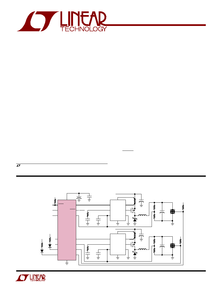
Dual Fan Controller
with 2-Wire Interface
1840 TA01
+
C
FB1
100pF
C
C1
220pF
R
SENSE1
0.05
R
SENSE2
0.05
R
FB1A
75k
R
FB1B
28k
C
OUT1
150
µ
F
+
DC
FAN
C
VIN1
22
µ
F
L1 47
µ
H
Si6447DQ
UPS5817
TACH
OUT
3.3V
3.3V
3.3V
3.3V
3.3V
GND
V
CC
+
C
FB2
100pF
C
C2
220pF
R
FB2A
75k
R
FB2B
28k
C
OUT2
150
µ
F
+
DC
FAN
C
VIN2
22
µ
F
L2 47
µ
H
Si6447DQ
UPS5817
TACH
OUT
3.3V
12V
12V
SYSTEM
RESET
GPI04
BLAST
IDACOUTA
GPI03
IDACOUTB
TACHB
TACHA
FAULT
SDA
SCL
A0
A1
GPI01
GPI02
LTC1840
R
C1
10k
R
C2
10k
TO
MASTER
NC
NC
130
LED1
130
LED2
ADDRESS = 1110010
(8 OTHERS POSSIBLE)
2-NMB 6820PL-04W-B29-D50 FANS
1.1A NOM AT 12V
10k
10k
10k
+
10
µ
F
0.1
µ
F
RUN/SS
I
TH
V
FB
GND
V
IN
SENSE
PGATE
MODE
LTC1771
RUN/SS
I
TH
V
FB
GND
V
IN
SENSE
PGATE
MODE
LTC1771
Low Parts Count, High Efficiency Dual Fan Control
, LTC and LT are registered trademarks of Linear Technology Corporation.
I
2
C is a trademark of Philips Electronics N.V.
LTC1840
2
1840f
TOP VIEW
GN PACKAGE
16-LEAD PLASTIC SSOP
1
2
3
4
5
6
7
8
16
15
14
13
12
11
10
9
SCL
SDA
A1
A0
FAULT
GPIO1
GPIO2
GND
V
CC
I
DACOUTA
I
DACOUTB
BLAST
TACHB
TACHA
GPIO4
GPIO3
V
CC
to GND .................................................... 0.3 to 6V
A0, A1 ............................................. 0.3 to (V
CC
+ 0.3V)
I
DACOUTA
, I
DACOUTB .............................
0.3 to (V
CC
+ 0.75V)
All other pins ................................................. 0.3 to 6V
Operating Temperature
LTC1840C ............................................... 0
°
C to 70
°
C
LTC1840I .............................................40
°
C to 85
°
C
Storage Temperature Range ..................65
°
C to 125
°
C
Lead Temperature (Soldering, 10 sec).................. 300
°
C
ORDER PART
NUMBER
GN PART
MARKING
T
JMAX
= 125
°
C,
JA
= 110
°
C/W
Consult LTC marketing for parts specified with wider operating temperature ranges.
1840
1840I
LTC1840CGN
LTC1840IGN
ABSOLUTE AXI U
RATI GS
W
W
W
U
PACKAGE/ORDER I FOR ATIO
U
U
W
(Note 1)
ELECTRICAL CHARACTERISTICS
The
q
denotes the specifications which apply over the full operating
temperature range, otherwise specifications are at T
A
= 25
°
C. V
CC
= 3V
SYMBOL
PARAMETER
CONDITIONS
MIN
TYP
MAX
UNITS
DACs
n
Resolution
8
Bits
DNL
Differential Nonlinearity
V
DACOUT
= 1.1V, Guaranteed Monotonic
q
±
0.9
LSB
INL
Integral Nonlinearity
V
DACOUT
= 1.1V
±
4
LSB
ZSE
Zero-Scale Error
V
DACOUT
= 1.1V
0.2
0.1
2
µ
A
Output Voltage Rejection
1.1V< V
DACOUT
< 3.75V
±
1
LSB
Output Voltage Rejection
V
CC
= 5.75V, 1.1V < V
DACOUT
< 6.5V
±
2
LSB
I
DACOUTA(FS),
Full-Scale Current
Sinking
97
103
µ
A
I
DACOUTB(FS)
V
DACOUT
= 1.1V
q
95
105
µ
A
Power Supply
V
CC
Positive Supply Voltage
q
2.7
5.75
V
I
CC
Supply Current
V
CC
= 3V, A0 and A1 Floating
400
600
µ
A
V
CC
= 5V, A0 and A1 Floating
500
750
µ
A
V
UVLO
UVLO/POR Voltage
q
2.1
2.4
2.69
V
V
UVHYS
UVLO/POR Voltage Hysteresis
(Note 2)
20
90
160
mV
Oscillator Performance
f
OSC
Oscillator Frequency
q
47
50
53
kHz
PSRR
Supply Sensitivity
2.7V < V
CC
< 5.75V
0.1
0.5
%/V
GPIO Performance
I
O
Output Current Sink
V
GPIOX
= 0.7V, Internal Pull-Down Enabled
q
10
mA
V
IL
Digital Input Low Voltage
Internal Pull-Down Disabled
q
0.3V
CC
V
V
IH
Digital Input High Voltage
Internal Pull-Down Disabled
q
0.7V
CC
V
V
IHYST
Input Hysteresis
(Note 2)
50
mV
I
LEAK
Leakage
Internal Pull-Down Disabled
±
1
µ
A
LTC1840
3
1840f
ELECTRICAL CHARACTERISTICS
The
q
denotes the specifications which apply over the full operating
temperature range, otherwise specifications are at T
A
= 25
°
C. V
CC
= 3V
Note 1: Absolute Maximum Ratings are those values beyond
which the life of a device may be impaired.
Note 2: Guaranteed by design not subject to test.
SYMBOL
PARAMETER
CONDITIONS
MIN
TYP
MAX
UNITS
Digital Inputs SCL, SDA
V
IH
Digital Input High Voltage
q
1.4
V
V
IL
Digital Input Low Voltage
q
0.6
V
V
LTH
Logic Threshold Voltage
(Note 2)
1
V
I
LEAK
Digital Input Leakage
V
CC
= 5V and 0V, V
IN
= GND to V
CC
±
1
µ
A
C
IN
Digital Input Capacitance
(Note 2)
10
pF
Digital Output SDA
V
OL
Digital Output Low Voltage
I
PULL-UP
= 3mA
q
0.4
V
Digital Output FAULT
V
OL
Digital Output Low Voltage
I
PULL-UP
= 1mA
q
0.4
V
Digital Inputs TACHA, TACHB
V
IH
Digital Input High Voltage
q
0.7V
CC
V
V
IL
Digital Input Low Voltage
q
0.3V
CC
V
I
LEAK
Digital Input Leakage
V
CC
= 5V and 0V, V
IN
= GND to V
CC
±
1
µ
A
Digital Input BLAST
V
LTH
Logic Threshold Voltage
Measured on BLAST Falling Edge
0.95
1.0
1.05
V
V
IHYST
Input Hysteresis
(Note 2), Measured on Rising Edge
20
mV
I
LEAK
Digital Input Leakage
V
CC
= 5V and 0V, V
IN
= GND to V
CC
±
1
µ
A
Address Inputs A0, A1
V
IH
Input High Voltage
q
0.9V
CC
V
V
IL
Input Low Voltage
q
0.1V
CC
V
I
IN
Input Current
AX Shorted to GND or V
CC
, V
CC
= 5V
±
100
µ
A
Timing Characteristics
f
I2C
I
2
C Operating Frequency
(Note 2)
0
100
kHz
t
BUF
Bus Free Time Between
(Note 2)
4.7
µ
s
Stop and Start Condition
t
hD, STA
Hold Time after (Repeated)
(Note 2)
4
µ
s
Start Condition
t
su, STA
Repeated Start Condition
(Note 2)
4.7
µ
s
Setup Time
t
su, STO
Stop Condition Setup Time
(Note 2)
4
µ
s
t
hD, DAT
Data Hold Time
300
ns
t
su, DAT
Data Setup Time
(Note 2)
250
ns
t
LOW
Clock Low Period
(Note 2)
4.7
µ
s
t
HIGH
Clock High Period
(Note 2)
4.0
µ
s
t
f
Clock, Data Fall Time
(Note 2)
300
ns
t
r
Clock, Data Rise Time
(Note 2)
1000
ns
LTC1840
4
1840f
TYPICAL PERFOR A CE CHARACTERISTICS
U
W
V
CC
(V)
2.5
I
CC
(
µ
A)
550
500
450
400
6.5
1840 G01
3.5
4.5
5.5
T
A
= 25
°
C
TEMPERATURE (
°
C)
50
I
CC
(
µ
A)
450
440
430
420
410
400
390
25
0
25
50
1840 G02
75
100
V
CC
(V)
2.5
I
DACOUT
(
µ
A)
100.00
100.05
6.5
1840 G03
99.95
99.90
3.5
4.5
5.5
100.10
T
A
= 25
°
C
V
DACOUT
(V)
0
I
DACOUT
(
µ
A)
120
100
80
60
40
20
0
1
2
3
4
1840 G04
5
6
T
A
= 25
°
C
V
DACOUT
(V)
0.5
100.10
100.05
100.00
99.95
99.90
99.85
99.80
99.75
3.5
1840 G05
1.5
2.5
4.5
I
DACOUT
(
µ
A)
T
A
= 25
°
C
V
DACOUT
(V)
I
DACOUT
(
µ
A)
100.5
100.3
100.1
99.9
99.7
99.5
99.3
99.1
1840 G06
0
1
2
3
4
5
6
T
A
= 25
°
C
FREQUENCY (kHz)
1
I
DACOUT
/V
CC
(
µ
A/V)
10
15
20
1840 G07
5
0
10
100
1000
T
A
= 25
°
C
TEMPERATURE (
°
C)
50
DAC ZSE (nA)
10
5
0
25
75
1840 G08
25
0
50
100
125
CODE
1
DNL (LSB)
0.2
0.1
0
0.1
0.2
255
1840 G09
T
A
= 25
°
C
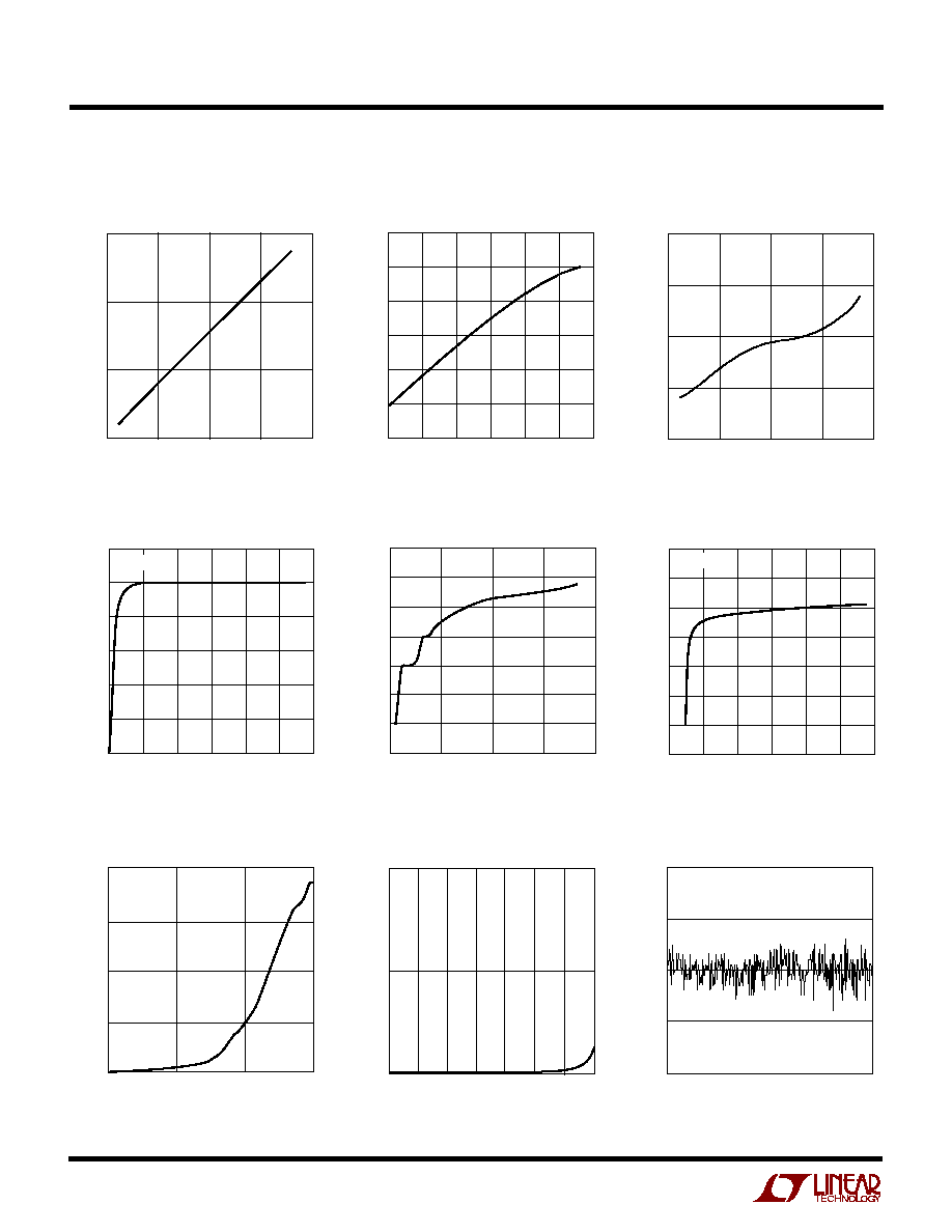
Supply Current vs Supply Voltage
Supply Current vs Temperature
(V
CC
= 3V)
I
DACOUT
Full Scale vs V
CC
,
V
DACOUT
= 1.1V
I
DACOUT
FS vs V
DACOUT
at V
CC
= 3V to 5V
I
DACOUT
FS vs V
DACOUT
at V
CC
= 3V
I
DACOUT
FS vs V
DACOUT
at V
CC
= 5V
I
DACOUT
AC Supply Rejection at
Full Scale, V
CC
= 3V DC
DAC Zero Scale Error at V
CC
= 3V,
V
DACOUT
= 1.1V
DAC DNL vs Code at V
CC
= 3V
LTC1840
5
1840f
fault conditions on the LTC1840. An external 10k pull-up
is recommended.
GPIO1, GPIO2, GPIO3, GPIO4 (Pins 6, 7, 9, 10): General
Purpose Inputs/Outputs. These pins can be used as digital
inputs with CMOS logic thresholds or digital outputs/LED
drivers with open drain pull-downs that can be pro-
grammed to blink. GPIO pins can be programmed to
produce faults due to changes in their logic states, and
these faults can only be cleared by software or powering
the LTC1840 down. All GPIOs default to nonfaulting logic
inputs upon power-up and their functionality is changed
through the serial interface.
GND (Pin 8): Ground. Connect to analog ground plane.
TACHA (Pin 11): Tachometer Input A. This pin is a digital
input that is designed to interface to the tachometer output
from a 3-wire fan. Internal logic counts between rising
TACHA edges at serially programmable frequencies of
25kHz, 12.5kHz, 6.25kHz or 3.125kHz and the most re-
cently completed count is stored in a register accessible
through the serial interface. The maximum count is 255
and the LTC1840 is programmable to produce faults when
a count exceeds this number. This pin has CMOS thresh-
olds and the default conditions are to count at 3.125kHz
and to not produce faults.
TACHB (Pin 12): Tachometer Input B. See TACHA
U
U
U
PI FU CTIO S
SCL (Pin 1): Serial Clock Input. The 2-wire bus master
device clocks this pin at a frequency between 0kHz and
100kHz to enable serial bus communications. Data at the
SDA pin is shifted in or out on rising SCL edges. SCL has
a logic threshold of 1V and an external pull-up resistor or
current source is normally required.
SDA (Pin 2): Serial Data Input. This is a bidirectional data
pin which normally has an external pull-up resistor or
current source and can be pulled down by the open drain
device on the LTC1840 or by external devices. The master
controls SDA during addressing, the writing of data, and
read acknowledgment, while the LTC1840 controls SDA
when data is being read back and during write acknowl-
edgment. SDA data is shifted in or out on rising SCL edges.
SDA has a logic threshold of 1V.
A1 (Pin 3): Three State Address Programming Input. This
pin can cause three different logic states internally, de-
pending upon whether it is pulled to supply, pulled to
ground, or not connected (NC). Combined with the A0 pin,
this provides for nine different possible two-wire bus
addresses for the LTC1840 (see Table 1).
A0 (Pin 4): Three State Address Programming Input. See
A1.
FAULT (Pin 5): Fault Indicator Pull-Down Output. This pin
has an open drain pull-down that is used to signal various
TYPICAL PERFOR A CE CHARACTERISTICS
U
W
CODE
0
BEST FIT INL (LSB)
0.4
0.3
0.2
0.1
0
0.1
0.2
255
1840 G10
T
A
= 25
°
C
TEMPERATURE (
°
C)
50
25
25
75
BLASTB THRESHOLD (V)
50
1.011
1.010
1.009
1.008
1.007
1.006
1.005
1.004
1.003
1.002
1840 G11
0
100
BLAST Falling Threshold
at V
CC
= 3V
DAC INL at V
CC
= 3V