Äîêóìåíòàöèÿ è îïèñàíèÿ www.docs.chipfind.ru
1
LTC1694
SMBus/I
2
C Accelerator
s
Improves SMBus Rise Time Transition
s
Ensures Data Integrity with Multiple Devices
on the SMBus
s
Improves Low State Noise Margin
s
Auto Detect Low Power Standby Mode
s
Wide Supply Voltage Range: 2.7V to 6V
s
Tiny 5-Pin SOT-23 Package
The LT C
®
1694 is a dual SMBus active pull-up designed to
enhance data transmission speed and reliability under all
specified SMBus loading conditions. The LTC1694 is also
compatible with the Philips I
2
C
TM
Bus.
The LTC1694 allows multiple device connections or a
longer, more capacitive interconnect, without compro-
mising slew rates or bus performance, by using two
bilevel hysteretic current source pull-ups.
During positive bus transitions, the LTC1694 current
sources provide 2.2mA to quickly slew the SMBus line.
During negative transitions or steady DC levels, the cur-
rent sources decrease to 275
µ
A to improve negative slew
rate and improve low state noise margins. An auto detect
standby mode reduces supply current if both SCL and
SDA are high.
The LTC1694 is available in a 5-pin SOT-23 package,
requiring virtually the same space as two surface mount
resistors.
s
Notebook and Palmtop Computers
s
Portable Instruments
s
Battery Chargers
s
Industrial Control Application
s
TV/Video Products
s
ACPI SMBus Interface
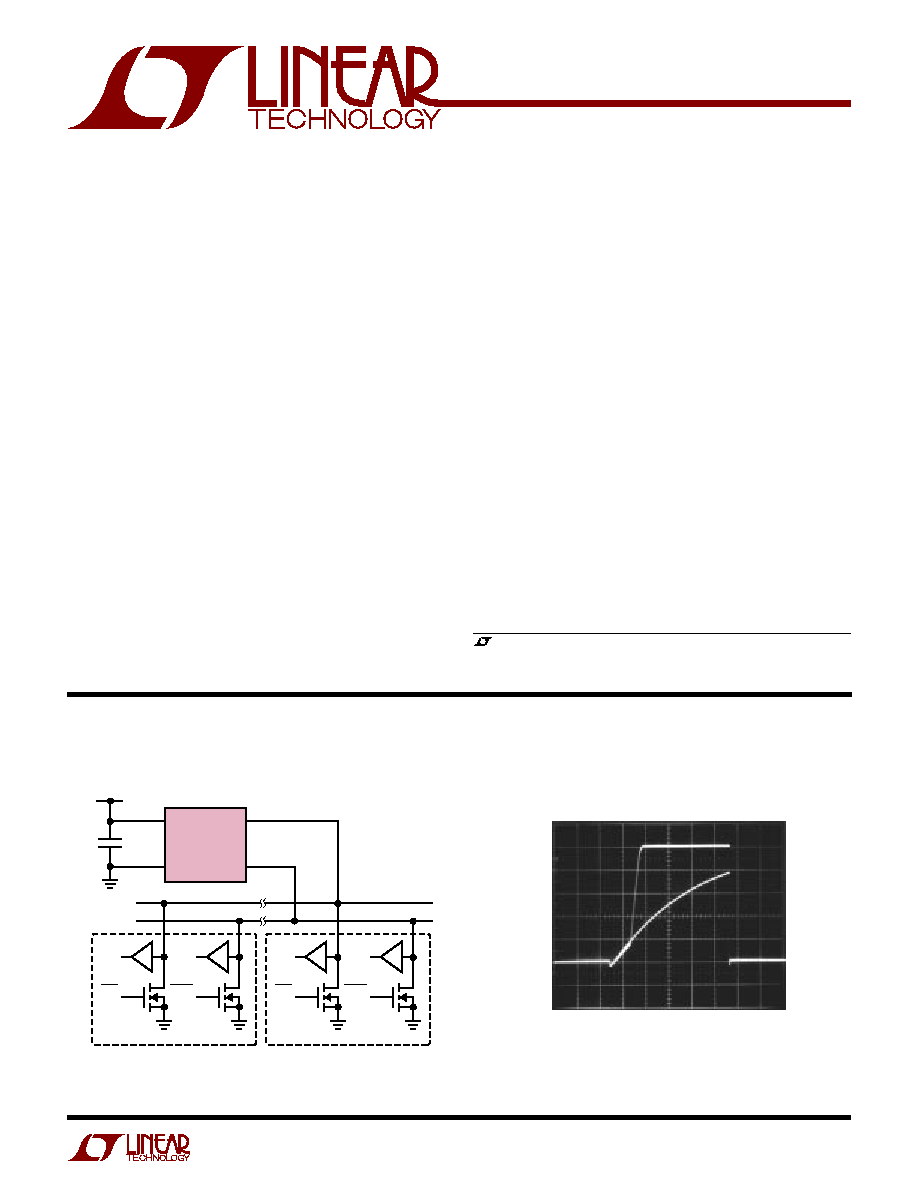
LTC1694
V
CC
GND
V
CC
5V
C1
0.1
µ
F
SMBus1
SMBus2
1
2
5
4
SCL
SDA
DEVICE 1
CLK
IN
CLK
OUT
SMBus
DATA
IN
DATA
OUT
DEVICE N
1694 TA01
CLK
IN
CLK
OUT
DATA
IN
DATA
OUT
, LTC and LT are registered trademarks of Linear Technology Corporation.
I
2
C is a trademark of Philips Electronics N.V.
V
CC
= 5V
1
µ
s/DIV
C
LD
= 200pF
f
SMBus
= 100kHz
1694 TA02
Comparison of SMBus Waveforms for
the LTC1694 vs Resistor Pull-Up
LTC1694
R
PULL-UP
= 15.8k
LTC1694: Patent Pending
FEATURES
DESCRIPTIO
U
APPLICATIO S
U
TYPICAL APPLICATIO
U
1V/DIV
2
LTC1694
ORDER PART
NUMBER
LTC1694CS5
(Note 1)
Supply Voltage (V
CC
) ................................................. 7V
SMBus1, SMBus2 Inputs ............ 0.3V to (V
CC
+ 0.3V)
Operating Ambient Temperature Range ....... 0
°
C to 70
°
C
Junction Temperature ........................................... 125
°
C
Storage Temperature Range ................. 65
°
C to 150
°
C
Lead Temperature (Soldering, 10 sec.)................. 300
°
C
V
CC
1
GND 2
NC 3
5 SMBus1
4 SMBus2
TOP VIEW
S5 PACKAGE
5-LEAD PLASTIC SOT-23
T
JMAX
= 125
°
C,
JA
= 256
°
C/ W
Consult factory for Industrial and Military grade parts.
LTEE
S5 PART MARKING
The
q
denotes specifications that apply over the full operating temperature range, otherwise specifications are at T
A
= 25
°
C.
V
CC
= 2.7V to 6V unless otherwise noted.
SYMBOL
PARAMETER
CONDITIONS
MIN
TYP
MAX
UNITS
V
CC
Supply Voltage Range
2.7
6
V
I
CC
Supply Current
SMBus1 = SMBus2 = Open
q
20
60
100
µ
A
I
PULL-UP
Pull-Up Current
SMBus1 = SMBus2 = 0V
q
125
275
350
µ
A
Boosted Pull-Up Current
Positive Transition on SMBus ( Figure 1)
q
1.0
2.2
mA
Slew Rate = 0.5V/
µ
s, SMBus > V
THRES
V
THRES
Input Threshold Voltage
Slew Rate = 0.5V/
µ
s (Figure 1)
q
0.4
0.65
0.9
V
SR
THRES
Slew Rate Detector Threshold
SMBus > V
THRES
q
0.2
0.5
V/
µ
s
t
r
SMBus Rise Time
Bus Capacitance = 200pF (Note 2)
q
0.32
1.0
µ
s
Standard Mode I
2
C Bus Rise Time
Bus Capacitance = 400pF (Note 3)
q
0.30
1.0
µ
s
f
MAX
SMBus Maximum Operating Frequency
(Note 4)
q
100
kHz
Note 1: Absolute Maximum Ratings are those values beyond which the life
of a device may be impaired.
Note 2: The rise time of an SMBus line is calculated from (V
IL(MAX)
0.15V) to (V
IH(MIN)
+ 0.15V) or 0.65V to 2.25V. This parameter is
guaranteed by design and not tested. With a minimum pull-up current of
125
µ
A, a minimum boosted pull-up current of 1mA and a maximum input
threshold voltage of 0.9V:
Rise Time = [(0.9V 0.65V)/125
µ
A + (2.25V 0.9V)/1mA] · 200pF
= 0.67
µ
s
Note 3: The rise time of an I
2
C bus line is calculated from V
IL(MAX)
to
V
IH(MIN)
or 1.5V to 3V (with V
CC
= 5V). This parameter is guaranteed by
design and not tested. With a minimum boosted pull-up current of 1mA:
Rise Time = (3V 1.5V) · 400pF/1mA = 0.6
µ
s
Note 4: This parameter is guaranteed by design and not tested.
ABSOLUTE AXI U RATI GS
W
W
W
U
PACKAGE/ORDER I FOR ATIO
U
U
W
ELECTRICAL CHARACTERISTICS
3
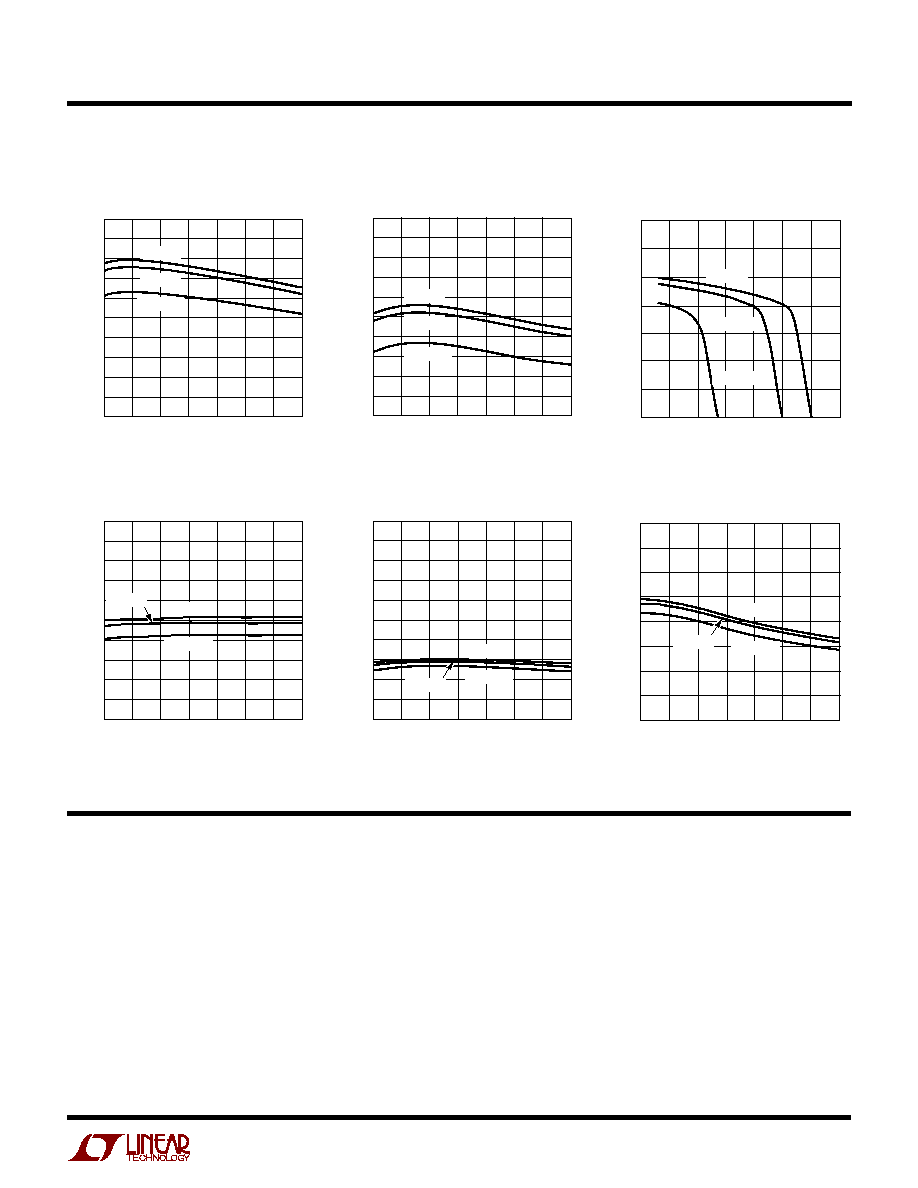
LTC1694
TEMPERATURE (
°
C)
50
PULL-UP CURRENT (
µ
A)
350
325
300
275
250
225
200
175
150
125
100
0
50
75
1694 G01
25
25
100
125
V
CC
= 6V
V
CC
= 5V
V
CC
= 2.7V
TEMPERATURE (
°
C)
50
BOOSTED PULL-UP CURRENT (mA)
3.50
3.25
3.00
2.75
2.50
2.25
2.00
1.75
1.50
1.25
1.00
0
50
75
1694 G02
25
25
100
125
V
CC
= 6V
V
CC
= 5V
V
CC
= 2.7V
Boosted Pull-Up Current vs
SMBus Voltage
TEMPERATURE (
°
C)
50
INPUT THRESHOLD VOLTAGE (V)
0.90
0.85
0.80
0.75
0.70
0.65
0.60
0.55
0.50
0.45
0.40
0
50
75
1694 G04
25
25
100
125
V
CC
= 6V
V
CC
= 2.7V
V
CC
= 5V
TEMPERATURE (
°
C)
50
SLEW RATE DETECTOR THRESHOLD (V/
µ
s)
0.50
0.45
0.40
0.35
0.30
0.25
0.20
0.15
0.10
0.05
0
0
50
75
1694 G05
25
25
100
125
V
CC
= 6V
V
CC
= 2.7V
V
CC
= 5V
Slew Rate Detector Threshold
Standby Mode Supply Current
TEMPERATURE (
°
C)
50
SUPPLY CURRENT (
µ
A)
100
1694 G06
0
50
100
90
80
70
60
50
40
30
20
25
25
75
125
V
CC
= 6V
V
CC
= 2.7V
V
CC
= 5V
Pull-Up Current at SMBus = 0V
Boosted Pull-Up Current
SMBus VOLTAGE (V)
0
3.5
3.0
2.5
2.0
1.5
1.0
0.5
0
3
5
LT
1694 G03
1
2
4
6
7
BOOSTED PULL-UP CURRENT (mA)
V
CC
= 6V
V
CC
= 5V
V
CC
= 2.7V
Input Threshold Voltage
TYPICAL PERFOR A CE CHARACTERISTICS
U
W
V
CC
(Pin 1): Power Supply Input. V
CC
can range from 2.7V
to 6V and requires a 0.1
µ
F bypass capacitor to GND.
GND (Pin 2): Ground.
NC (Pin 3): No Connection.
SMBus2 (Pin 4): Active pull-up for SMBus.
SMBus1 (Pin 5): Active pull-up for SMBus.
U
U
U
PI FU CTIO S
4
LTC1694
+
SLEW RATE
DETECTOR
CONTROL
LOGIC
0.65V
V
REF
VOLTAGE
COMP
1.925mA
STANDBY
CHANNEL ONE
CHANNEL TWO
(DUPLICATE OF CHANNEL ONE)
1694 BD
1
175
µ
A
100
µ
A
V
CC
5
SMBus1
SMBus2
2
GND
4
BLOCK DIAGRA
W
Figure 1
LTC1694
V
CC
GND
V
CC
5V
C1
0.1
µ
F
SMBus1
SMBus2
5
4
1
2
HP5082-2080
TEST RAMP VOLTAGE
BSS284
V
R
1k
10V
1694 f01a
+
LT1360
BOOSTED PULL-UP
2.2mA (TYP)
275
µ
A
(TYP)
TEST RAMP
VOLTAGE
0
µ
A
V
CC
1694 F01b
0.5V/
µ
s
0V
V
THRES
I
PULL-UP
=
V
R
1k
TEST CIRCUITS

5
LTC1694
SMBus Overview
SMBus communication protocol employs open-drain
drivers with resistive or current source pull-ups. This
protocol allows multiple devices to drive and monitor the
bus without bus contention. The simplicity of resistive or
fixed current source pull-ups is offset by the slow rise
times they afford when bus capacitance is high. Rise
times can be improved by using lower pull-up resistor
values or higher fixed current source values, but the
additional current increases the low state bus voltage,
decreasing noise margins. Slow rise times can seriously
impact data reliability, enforcing a maximum practical
bus speed well below the established SMBus maximum
transmission rate.
Theory of Operation
The LTC1694 overcomes these limitations by using bilevel
hysteretic current sources as pull-ups. During positive
SMBus line transitions, the pull-up current sources typi-
cally provide 2.2mA to quickly slew any parasitic bus
capacitance. Therefore, rise time is dramatically improved,
especially with maximum SMBus loading conditions.
The LTC1694 has separate but identical circuitry for each
SMBus output pin. The circuitry consists of a positive edge
slew rate detector and a voltage comparator.
The LTC1694 nominally sources only 275
µ
A of pull-up
current to maintain good V
OL
noise margin. The 2.2mA
boosted pull-up current is only turned on if the voltage on
the SMBus line voltage is greater than the 0.65V compara-
tor threshold voltage and the positive slew rate of the
SMBus line is greater than the 0.2V/
µ
s threshold of the
slew rate detector. The boosted pull-up current remains on
until the voltage on the SMBus line is within 0.5V of V
CC
and/or the slew rate drops below 0.2V/
µ
s.
Auto Detect Standby Mode
The LTC1694 enters standby mode if the voltage on both
the SCL and SDA lines is high (idle state). In standby mode,
the pull-up currents drop to 100
µ
A, thereby lowering the
system power consumption.
Maximum R
S
Considerations
For ESD protection of the SMBus lines, a series resistor R
S
(Figure 2) is sometimes added to the open-drain driver of
the bus agents. This is especially common in SMBus-
controlled smart batteries. The maximum value of R
S
is
limited by the low state noise margin and timing require-
ments of the SMBus specification. The maximum value for
R
S
is 700
if resistive pull-ups or fixed value current
sources are used.
In general, an R
S
of 100
to 200
is sufficient for ESD
protection while meeting both the low state noise margin
and fall time requirement. If a larger value of R
S
is required,
take care to ensure that the low state noise margin and
timing requirement of the SMBus specification is not
violated. Also, the fall time of an SMBus line will also be
increased by using a high value series resistor.
APPLICATIO S I FOR ATIO
W
U
U
U
SDA
R
S
R
ON
1694 F02
DATA
IN
DATA
OUT
Figure 2
Low State Noise Margin
An acceptable V
OL
noise margin is easily achieved with the
low pull-up current (350
µ
A maximum) of the LTC1694.
The maximum value of R
S
is calculated from a desired low
state noise margin (NM
L
):
R
V
NM
I
R
S MAX
OL MAX
L
PU
MAX
ON MAX
(
)
(
)
(
)
(
)
=
-
-
LL-UP
(1)
V
OL(MAX)
:
The maximum V
OL
of the SMBus specifica-
tion is 0.4V