1503i.pm6 copy
1
LTC1503-1.8/LTC1503-2
High Efficiency Inductorless
Step-Down DC/DC Converters
s
Input Voltage Range: 2.4V to 6V
s
Fixed Output Voltages: 1.8V
±
4%, 2V
±
4%
s
Output Current: Up to 100mA
s
No Inductors
s
Typical Efficiency 25% Higher than LDOs
s
Low Operating Current: 25
µ
A
s
Low Shutdown Current: 5
µ
A
s
600kHz Switching Frequency
s
Shutdown Disconnects Load from V
IN
s
Soft-Start Limits Inrush Current at Turn-On
s
Short-Circuit and Overtemperature Protected
s
Available in 8-Pin MSOP and SO Packages
The LTC
®
1503-1.8/LTC1503-2 are switched capacitor
step-down DC/DC converters that produce a regulated
output from a 2.4V to 6V input. The parts use switched
capacitor fractional conversion to achieve high efficiency
over the entire input range. No inductors are required.
Internal circuitry controls the step-down conversion ratio
to optimize efficiency as the input voltage and load condi-
tions vary. Typical efficiency is 25% higher than that of a
low dropout (LDO) linear regulator.
Regulation is achieved by sensing the output voltage and
enabling the internal switching network as needed to
maintain a fixed output voltage. This method of regulation
enables the parts to achieve high efficiency at extremely
light loads. Low operating current (25
µ
A with no load, 5
µ
A
in shutdown) and low external parts count (two 1
µ
F flying
capacitors and two 10
µ
F bypass capacitors) make the
LTC1503-1.8/LTC1503-2 ideally suited for space con-
strained battery-powered applications. The parts are fully
short-circuit and overtemperature protected.
The LTC1503-1.8/LTC1503-2 are available in 8-pin MSOP
and SO packages.
, LTC and LT are registered trademarks of Linear Technology Corporation.
s
Cellular Phones
s
Handheld Computers
s
Smart Card Readers
s
Low Power DSP Supplies
s
Portable Electronic Equipment
s
Handheld Medical Instruments
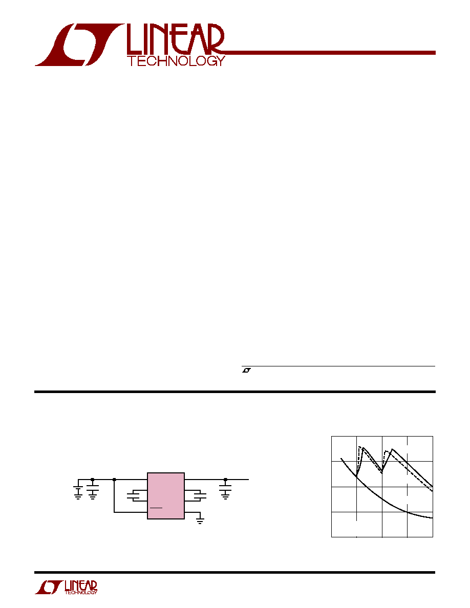
Efficiency vs Input Voltage
Single Li-Ion to 2V DC/DC Converter
FEATURES
DESCRIPTIO
U
APPLICATIO S
U
TYPICAL APPLICATIO
U
4
2
3
5
1
8
6
7
V
IN
C1
C1
+
SHDN/SS
V
OUT
C2
C2
+
GND
LTC1503-2
1
µ
F
1503-1.8/2 TA01
1
µ
F
10
µ
F
1-CELL Li-Ion OR
3-CELL NiMH
10
µ
F
V
OUT
= 2V
I
OUT
= 100mA
INPUT VOLTAGE (V)
2
EFFICIENCY (%)
60
80
6
1503-1.8/2 TA02
40
20
3
4
5
100
LTC1503-2
V
OUT
= 2V
I
OUT
= 100mA
I
OUT
= 1mA
"IDEAL" LDO
2
LTC1503-1.8/LTC1503-2
Industrial Temperature Range ............... 40
°
C to 85
°
C
Specified Temperature Range (Note 2) ... 40
°
C to 85
°
C
Storage Temperature Range ................ 65
°
C to 150
°
C
Lead Temperature (Soldering, 10 sec)................. 300
°
C
(Note 1)
PARAMETER
CONDITIONS
MIN
TYP
MAX
UNITS
V
IN
Operating Voltage
q
2.4
6
V
V
OUT
LTC1503-1.8, 0mA < I
OUT
< 100mA
q
1.728
1.8
1.872
V
LTC1503-2, 0mA < I
OUT
< 100mA
q
1.920
2.0
2.080
V
V
IN
Operating Current
I
OUT
= 0mA
q
25
50
µ
A
V
IN
Shutdown Current
SHDN/SS = 0V
q
5
10
µ
A
Output Ripple Voltage
LTC1503-X, V
IN
= 3.6V, I
OUT
= 100mA
25
mV
P-P
Efficiency
LTC1503-2, V
IN
= 3.6V, I
OUT
= 100mA
82.9
%
Switching Frequency
Oscillator Free Running
600
kHz
SHDN/SS Input Threshold
q
0.2
0.35
0.5
V
SHDN/SS Input Current
V
SHDN/SS
= 0V (Note 3)
q
3.5
2
1
µ
A
V
SHDN/SS
= V
IN
q
1
1
µ
A
V
OUT
Short-Circuit Current
V
OUT
= 0V (Note 4)
q
8
22
50
mA
V
OUT
Turn-On Time
C
SS
= 0nF, V
IN
= 3.6V, C
OUT
= 10
µ
F
0.1
ms
C
SS
= 10nF
8
ms
Note 1: Absolute Maximum Ratings are those values beyond which the life
of a device may be impaired.
Note 2: The LTC1503C is guaranteed to meet specified performance from
0
°
C to 70
°
C and is designed, characterized and expected to meet these
extended temperature limits, but are not tested at 40
°
C and 85
°
C. The
LTC1503I is guaranteed to meet the extended temperature limits.
Note 3: Currents flowing into the device are positive polarity. Currents
flowing out of the device are negative polarity.
Note 4: When V
OUT
is less than 150mV, I
OUT
is limited to much less than
the maximum rated output current to prevent damage to the output
devices.
ORDER PART
NUMBER
LTC1503CMS8-1.8
LTC1503CMS8-2
MS8 PART MARKING
LTFX
LTHN
ORDER PART
NUMBER
LTC1503CS8-1.8
LTC1503CS8-2
LTC1503IS8-1.8
LTC1503IS8-2
S8 PART MARKING
150318
15032
Consult factory for Military grade parts.
T
JMAX
= 125
°
C,
JA
= 200
°
C/W
1
2
3
4
V
OUT
C1
C1
+
V
IN
8
7
6
5
C2
GND
C2
+
SHDN/SS
TOP VIEW
MS8 PACKAGE
8-LEAD PLASTIC MSOP
T
JMAX
= 125
°
C,
JA
= 150
°
C/W
1
2
3
4
8
7
6
5
TOP VIEW
S8 PACKAGE
8-LEAD PLASTIC SO
V
OUT
C1
C1
+
V
IN
C2
GND
C2
+
SHDN/SS
V
IN
, C1
+
, C1
, C2
+
, C2
to GND ............... 0.3V to 6.5V
SHDN/SS to GND ......................... 0.3V to (V
IN
+ 0.3V)
V
OUT
Short-Circuit Duration ............................. Indefinite
Commercial Temperature Range ............ 40
°
C to 85
°
C
The
q
denotes specifications which apply over the full operating temperature range, otherwise specifications are at T
A
= 25
°
C.
V
IN
= V
IN(MIN)
to V
IN(MAX)
, C1 = C2 = 1
µ
F, C
IN
= C
OUT
= 10
µ
F unless otherwise noted.
503I18
1503I2
ABSOLUTE AXI U RATI GS
W
W
W
U
PACKAGE/ORDER I FOR ATIO
U
U
W
ELECTRICAL CHARACTERISTICS
3
LTC1503-1.8/LTC1503-2
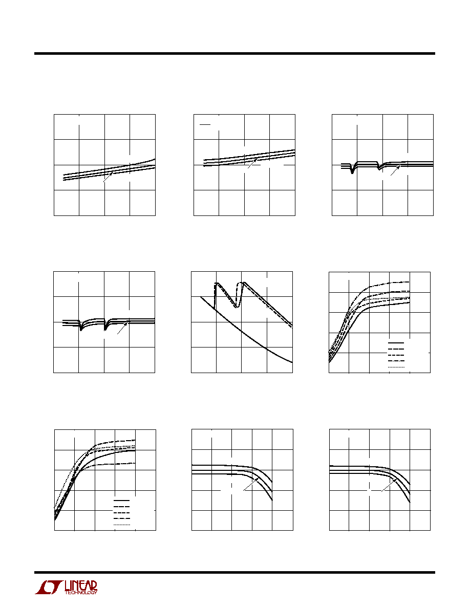
LTC1503-X Input Operating
Current vs Input Voltage
INPUT VOLTAGE (V)
2
INPUT CURRENT (
µ
A)
30
T
A
= 25
°
C
40
6
1503 G01
20
10
3
4
5
50
I
OUT
= 0mA
T
A
= 40
°
C
T
A
= 85
°
C
LTC1503-1.8
Output Voltage vs Input Voltage
LTC1503-2
Output Voltage vs Input Voltage
LTC1503-1.8
Efficiency vs Input Voltage
INPUT VOLTAGE (V)
2
OUTPUT VOLTAGE (V)
2.00
2.05
6
1503 G03
1.95
1.90
3
4
5
2.10
I
OUT
= 50mA
T
A
= 40
°
C
T
A
= 85
°
C
T
A
= 25
°
C
INPUT VOLTAGE (V)
2
EFFICIENCY (%)
60
80
6
1503-1.8/2 G05
40
20
3
4
5
100
"IDEAL"
LDO
T
A
= 25
°
C
I
OUT
= 100mA
I
OUT
= 1mA
LTC1503-1.8
Efficiency vs Output Current
LTC1503-X Input Shutdown
Current vs Input Voltage
INPUT VOLTAGE (V)
2
INPUT SHUTDOWN CURRENT (
µ
A)
5
7.5
6
1503-1.8/2 TA02
2.5
0
3
4
5
10
V
OUT
= 0V
V
SHDN
/SS = 0V
T
A
= 40
°
C
T
A
= 85
°
C
T
A
= 25
°
C
INPUT VOLTAGE (V)
2
OUTPUT VOLTAGE (V)
1.80
1.85
6
1503-1.8/2 G03
1.75
1.70
3
4
5
1.90
I
OUT
= 50mA
T
A
= 40
°
C
T
A
= 85
°
C
T
A
= 25
°
C
OUTPUT CURRENT (mA)
0.01
EFFICIENCY (%)
60
80
100
100
1503-1.8/2 G06
40
20
0
0.1
1
10
1000
V
IN
= 5V
V
IN
= 4.4V
V
IN
= 3.6V
V
IN
= 3V
V
IN
= 2.4V
T
A
= 25
°
C
LTC1503-2
Efficiency vs Output Current
OUTPUT CURRENT (mA)
0.01
EFFICIENCY (%)
60
80
100
100
1503-1.8/2 G07
40
20
0
0.1
1
10
1000
V
IN
= 5V
V
IN
= 4.4V
V
IN
= 3.6V
V
IN
= 3V
V
IN
= 2.4V
T
A
= 25
°
C
LTC1503-1.8
Output Voltage vs Output Current
OUTPUT CURRENT (mA)
0.01
OUTPUT VOLTAGE (V)
1.80
1.82
1.84
100
1503-1.8/2 G08
1.78
1.76
1.74
0.1
1
10
1000
V
IN
= 3.3V
T
A
= 40
°
C
T
A
= 85
°
C
T
A
= 25
°
C
LTC1503-2
Output Voltage vs Output Current
OUTPUT CURRENT (mA)
0.01
OUTPUT VOLTAGE (V)
2.00
2.02
2.04
100
1503-1.8/2 G09
1.98
1.96
1.94
0.1
1
10
1000
V
IN
= 3.3V
T
A
= 40
°
C
T
A
= 85
°
C
T
A
= 25
°
C
TYPICAL PERFOR A CE CHARACTERISTICS
U
W
4
LTC1503-1.8/LTC1503-2
TYPICAL PERFOR A CE CHARACTERISTICS
U
W
LTC1503-X Output Short-Circuit
Current vs Input Voltage
LTC1503-X Start-Up Time
vs Soft-Start Capacitor
INPUT VOLTAGE (V)
2
OUTPUT CURRENT (mA)
20
30
6
1503-1.8/2 G10
10
0
3
4
5
40
V
OUT
SHORTED TO GND
T
A
= 40
°
C
T
A
= 85
°
C
T
A
= 25
°
C
SOFT-START CAPACITOR (nF)
0.01
START-UP TIME (ms)
1
10
100
1503-1.8/2 G10
0.1
0.01
0.1
1
10
100
V
IN
= 3.6V
T
A
= 40
°
C
T
A
= 25
°
C
T
A
= 85
°
C
Output Load Transient Response
(LTC1503-1.8,1mA to 100mA Step)
I
OUT
50mA/DIV
V
OUT
50mV/DIV
AC COUPLED
100mA
1mA
1ms/DIV
1503-1.8/2 G12
Output Ripple, C
OUT
= 10
µ
F
V
OUT
10mV/DIV
AC COUPLED
5
µ
s/DIV
1503-1.8/2 G13
V
IN
= 3.6V
V
OUT
= 2V
I
OUT
= 100mA
C
OUT
= 10
µ
F CERAMIC
Output Ripple, C
OUT
= 22
µ
F
V
OUT
10mV/DIV
AC COUPLED
5
µ
s/DIV
1503-1.8/2 G14
V
IN
= 3.6V
V
OUT
= 2V
I
OUT
= 100mA
C
OUT
= 22
µ
F CERAMIC
V
OUT
(Pin 1): Regulated Output Voltage. V
OUT
is discon-
nected from V
IN
during shutdown. Bypass V
OUT
to ground
with a
10
µ
F low ESR capacitor.
C1
(Pin 2): Flying Capacitor One Negative Terminal.
C1
+
(Pin 3): Flying Capacitor One Positive Terminal.
V
IN
(Pin 4): Input Voltage. V
IN
may be between 2.4V and
6V. Bypass V
IN
to ground with a
10
µ
F low ESR capacitor.
SHDN/SS (Pin 5): Shutdown/Soft-Start Control. The pin
is designed to be driven with an external open-drain
output. Holding the SHDN/SS pin below 0.25V will force
the part into shutdown mode. An internal pull-up current
of 2
µ
A will force the SHDN/SS voltage to climb to V
IN
once
the device driving the pin is forced into a Hi-Z state. To
limit inrush current on start-up, connect a capacitor
between the SHDN/SS pin and ground. Capacitance on
the SHDN/SS pin will limit the dV/dt of the pin during turn-
on which, in turn, will limit the dV/dt of V
OUT
. By selecting
an appropriate soft-start capacitor for a known output
capacitor, the user can control the inrush current during
U
U
U
PI FU CTIO S
5
LTC1503-1.8/LTC1503-2
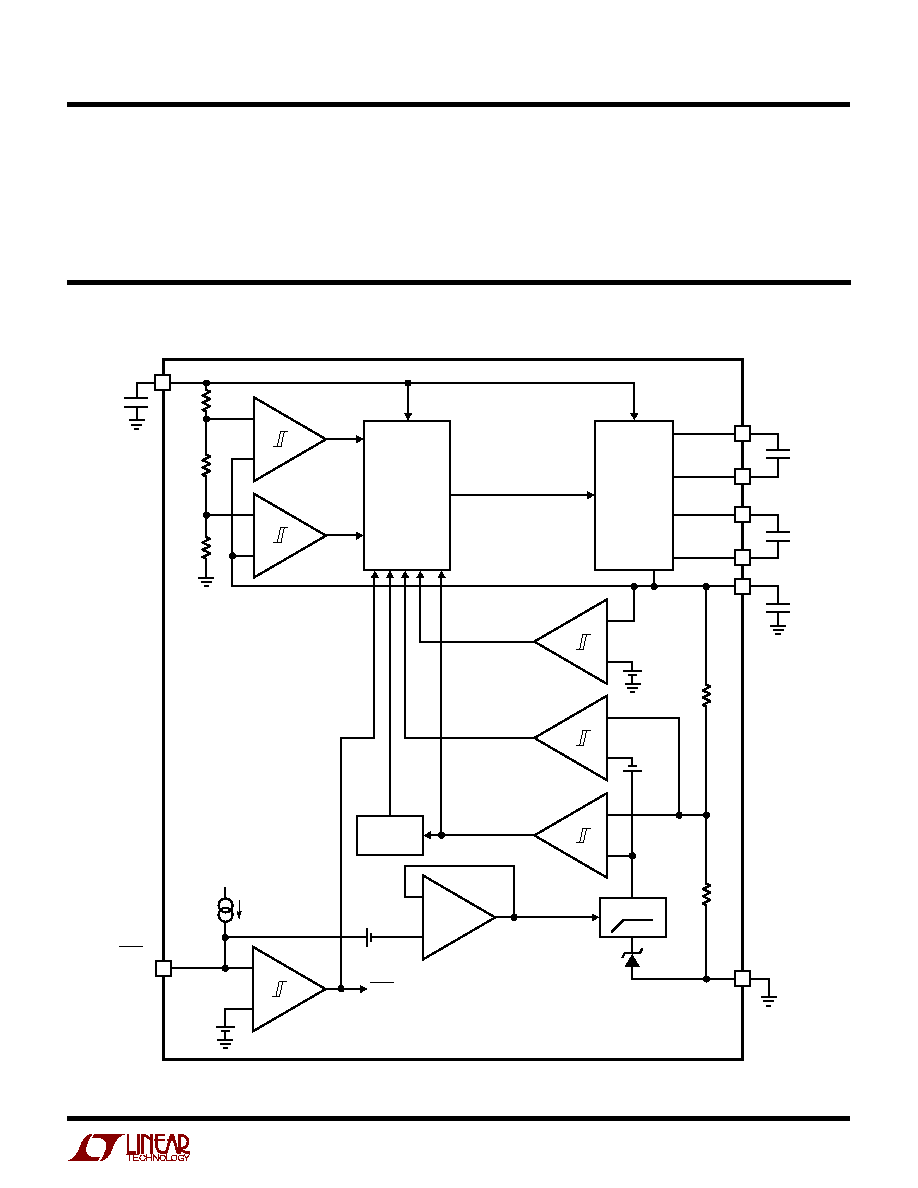
C1
+
V
IN
C1
C2
+
C2
150mV
800k
680k
330k
990k
1.2M
1.2V
V
REF
C
OUT
C
IN
V
OUT
GND
1503-1.8/2 BD
SHDN/SS
+
+
+
+
350mV
+
+
10mV
COMP2
MODE SKIP
REG ENABLE
SOFT-START
LTC1503-2
SHORT CIRCUIT
V
OUT
+
COMP1
350mV
V
IN
SHDN
2
µ
A
+
V
REF
RAMP
+
+
STEP-DOWN
CHARGE
PUMP
MODE
CONTROL
600kHz
OSCILLATOR
+
turn-on (see Applications Information). If neither of the
two functions are desired, the pin may be floated or tied
to V
IN
.
C2
+
(Pin 6): Flying Capacitor Two Positive Terminal.
GND (Pin 7): Ground. Connect to a ground plane for best
performance.
C2
(Pin 8): Flying Capacitor Two Negative Terminal.
U
U
U
PI FU CTIO S
BLOCK DIAGRA
W