Äîêóìåíòàöèÿ è îïèñàíèÿ www.docs.chipfind.ru
1
LTC1426
Micropower
Dual 6-Bit PWM DAC
FEATURES
DESCRIPTIO
N
U
s
Wide Supply Range: 2.7V
V
CC
5.5V
s
Wide Reference Voltage Range: 0V to 5.5V
s
Two Interface Modes:
Pulse Mode (Increment Only)
Pushbutton Mode (Increment/Decrement)
s
Low Supply Current: 50
µ
A
s
0.2
µ
A Supply Current in Shutdown
s
Available in 8-Pin MSOP and SO Packages
s
DAC Contents Are Retained in Shutdown
s
DACs Power-Up at Midrange
s
Low Output Impedance: < 100
s
Output Frequency: 5kHz Typ
The LTC
®
1426 is a dual micropower 6-bit PWM DAC
featuring versatile PWM outputs and a flexible pushbutton
compatible digital interface. The DAC outputs provide a
PWM signal that swings from 0V to V
REF
, allowing the full-
scale output to be varied by adjusting the voltage at V
REF
.
The PWM output frequency is typically 5kHz, easing
output filtering requirements. V
CC
supply current is typi-
cally 50
µ
A and drops to 0.2
µ
A in shutdown.
The LTC1426 can be controlled using one of two interface
modes: pushbutton and pulse. The LTC1426 automati-
cally configures itself into the appropriate mode at start-
up by monitoring the state of the CLK pins. In pushbutton
mode, the CLK pins can be directly connected to external
pushbuttons to control the DAC output. In pulse mode,
the CLK pins can be connected to CMOS compatible
logic. The DAC outputs initially power up at half scale and
the contents of the internal DAC registers are retained in
shutdown.
The LTC1426 is available in 8-pin MSOP and SO packages.
, LTC and LT are registered trademarks of Linear Technology Corporation.
s
LCD Contrast and Backlight Brightness Control
s
Power Supply Voltage Adjustment
s
Battery Charger Voltage and Current Adjustment
s
GaAs FET Bias Adjustment
s
Trimmer Pot Elimination
APPLICATIO
N
S
U
TYPICAL APPLICATIO
N
U
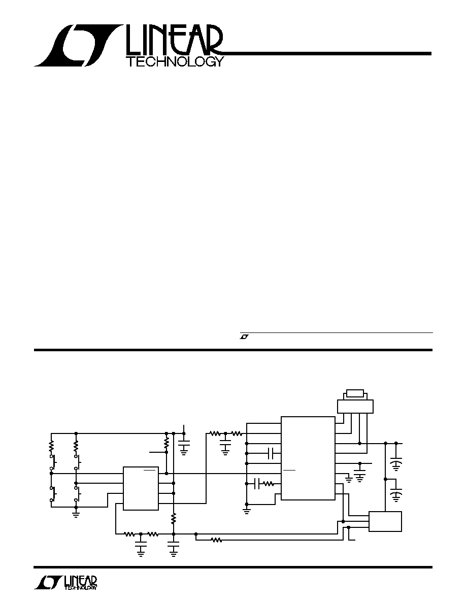
Pushbutton Adjustable CCFL/LCD Contrast Generator
1
2
3
4
8
7
6
5
CLK1
CLK2
GND
PWM1
SHDN
V
CC
V
REF
PWM2
LTC1426
1
2
3
4
5
6
7
8
16
15
14
13
12
11
10
9
CCFL PGND
I
CCFL
DIO
CCFL V
C
AGND
SHDN
LCD V
C
LCD PGND
CCFL V
SW
BULB
BAT
ROYER
V
IN
FBP
FBN
LCD V
SW
LT1182
1426 TA01
C4
0.1
µ
F
5V
DOWN
CONTRAST
UP/DOWN
CCFL UP/DOWN
DOWN
UP
UP
R
P1
47k
R
P2
47k
R
SHDN
1M
SHDN
R5
20k
1%
R6
40k
1%
R4
4.99k
1%
R3
5.1k
1%
R1
44.2k
1%
R2
44.2k
1%
UP TO 6mA
I
CCFL
= 0
µ
A TO 50
µ
A
C3
10
µ
F
C9
2.2
µ
F
5V
CONSULT THE LT1182 DATA SHEET FOR
DETAILS ON THE HIGH VOLTAGE ROYER
AND LCD CONTRAST CONVERTER SECTIONS
C2
1
µ
F
C10
2.2
µ
F
35V
8V TO
28V
C1
0.1
µ
F
C8
0.68
µ
F
C7 1
µ
F
R7
10k
HIGH VOLTAGE
ROYER
LAMP
LCD
CONTRAST
CONVERTER
V
OUT
NEGATIVE
LCD CONTRAST
V
OUT
= 10V TO 30V
+
C11
2.2
µ
F
35V
+
2
LTC1426
ABSOLUTE
M
AXI
M
U
M
RATINGS
W
W
W
U
PACKAGE/ORDER I
N
FOR
M
ATIO
N
W
U
U
(Note 1)
Total Supply Voltage (V
CC
) ........................................ 7V
Reference Voltage (V
REF
) ............................... 0.3 to 7V
Input Voltage (All Inputs) .............. 0.3 to (V
CC
+ 0.3V)
DAC Output Short-Circuit Duration .................. Indefinite
I
PWM(MAX)
.......................................................... 100mA
Operating Temperature Range
LTC1426C................................................ 0
°
C to 70
°
C
LTC1426I ........................................... 40
°
C to 85
°
C
Storage Temperature Range ................. 65
°
C to 150
°
C
Lead Temperature (Soldering, 10 sec).................. 300
°
C
ORDER PART
NUMBER
MS8 PART MARKING
LTC1426CMS8
LTC1426CS8
LTC1426IS8
S8 PART MARKING
1426
1426I
LTBQ
1
2
3
4
8
7
6
5
TOP VIEW
S8 PACKAGE
8-LEAD PLASTIC SO
MS8 PACKAGE
8-LEAD PLASTIC MSOP
CLK1
CLK2
GND
PWM1
SHDN
V
CC
V
REF
PWM2
T
JMAX
= 100
°
C,
JA
= 200
°
C/ W (MS8)
T
JMAX
= 100
°
C,
JA
= 130
°
C/ W (S8)
Consult factory for Military grade parts.
ELECTRICAL CHARACTERISTICS
T
A
= 25
°
C, (Note 2) unless otherwise specified.
SYMBOL
PARAMETER
CONDITIONS
MIN
TYP
MAX
UNITS
V
CC
Supply Voltage
q
2.7
5.5
V
V
REF
Reference Voltage
q
0
5.5
V
I
CC
Supply Current
Pulse Mode: V
SHDN
= V
CC
, V
CLK1
= V
CLK2
= 0V, PWM1 = PWM2 = NC
q
40
100
µ
A
Pushbutton Mode: V
SHDN
= V
CC
, V
CLK1
= V
CLK2
= PWM1 = PWM2 = NC
q
50
100
µ
A
SHDN = 0 (Note 3)
q
0.2
±
10
µ
A
I
REF
Reference Current
Pulse Mode: V
SHDN
= V
CC
, V
CLK1
= V
CLK2
= 0V, PWM1 = PWM2 = NC
q
75
150
µ
A
Pushbutton Mode: V
SHDN
= V
CC
, V
CLK1
= V
CLK2
= PWM1 = PWM2 = NC
q
75
150
µ
A
SHDN = 0 (Note 3)
q
0.2
±
10
µ
A
DAC Resolution
6
bits
DAC Frequency
0
°
C
T
A
70
°
C
q
3
5
6
kHz
40
°
C
T
A
85
°
C
q
2
5
6
kHz
DAC Output Impedance
V
CC
= 2.7V, V
REF
= 0.5V
q
20
100
DAC Full-Scale Duty Cycle
98.44
%
DAC Zero-Scale Duty Cycle
0
%
DNL
DAC Differential Nonlinearity
Monotonicity Guaranteed (Note 4)
q
±
0.05
LSB
INL
DAC Integral Nonlinearity
(Note 4)
q
±
0.05
LSB
FS Error
DAC Full-Scale Error
q
±
0.50
LSB
I
IN
Logic Input Current
Pulse Mode: 0V
V
IN
V
CC
SHDN
q
±
5
µ
A
CLK1, CLK2
q
±
5
µ
A
Pushbutton Mode: 0V
V
IN
V
CC
SHDN
q
±
5
µ
A
CLK1, CLK2
q
±
10
µ
A
V
IH
CLK High Level
V
CC
= 5.5V
SHDN
q
2.0
V
Input Voltage (Note 5)
CLK1, CLK2
q
4.4
V
V
CC
= 3.6V
SHDN
q
1.9
V
CLK1, CLK2
q
2.9
V
3
LTC1426
SYMBOL
PARAMETER
CONDITIONS
MIN
TYP
MAX
UNITS
V
IL
CLK Low Level
V
CC
= 4.5V
SHDN
q
0.8
V
Input Voltage (Note 5)
CLK1, CLK2
q
0.8
V
V
CC
= 2.7V
SHDN
q
0.45
V
CLK1, CLK2
q
0.45
V
I
OZ
Three-State Output Leakage
SHDN = 0
q
±
5
µ
A
Z
IN
CLK Input Resistance
Pushbutton Mode, CLK1/CLK2
2.5
M
f
CLK
Clock Frequency
Pulse Mode, V
CC
= 3.3V
q
1
MHz
Pulse Mode, V
CC
= 2.7V
q
750
kHz
t
CKHI
Clock High Time
Pulse Mode, V
CC
= 3.3V
q
450
ns
Pulse Mode, V
CC
= 2.7V
q
600
ns
t
CKLO
Clock Low Time
Pulse Mode, V
CC
= 3.3V
q
450
ns
Pulse Mode, V
CC
= 2.7V
q
600
ns
t
PW
Pulse Width
Pushbutton Mode
q
670
µ
s
t
DEB
Debounce Time
Pushbutton Mode
q
10.7
12.8
21.3
ms
t
DELAY
Repeat Rate Delay
Pushbutton Mode
q
340
410
680
ms
f
REPEAT
Repeat Frequency
Pushbutton Mode
q
11.7
19.5
23.4
Hz
ELECTRICAL CHARACTERISTICS
T
A
= 25
°
C, (Note 2) unless otherwise specified.
Note 3: Shutdown current can be negative due to leakage currents if V
CC
>
V
REF
or V
REF
> V
CC
.
Note 4: Guaranteed by Design. Decouple the V
CC
and V
REF
pins to GND
using high quality, low ESR, low ESL 0.1
µ
F capacitors to eliminate PWM
switching noise that may otherwise get coupled into the CLK1/CLK2 high
impedance input buffers. The decoupling capacitors should be located in
close proximity to these pins and the ground line to have maximum effect.
Note 5: Input thresholds apply for both pushbutton and pulse modes.
The
q
denotes the specifications which apply over the full operating
temperature range.
Note 1: Absolute Maximum Ratings are those values beyond which the life
of the device may be impaired.
Note 2: All currents into device pins are positive; all currents out of device
pins are negative. All voltages are referenced to ground, unless otherwise
specified. All typicals are given for V
CC
= V
REF
= 5V, T
A
= 25
°
C and
PWM1/PWM2 output to GND, C
PWM
= 10pF.
TYPICAL PERFOR
M
A
N
CE CHARACTERISTICS
U
W
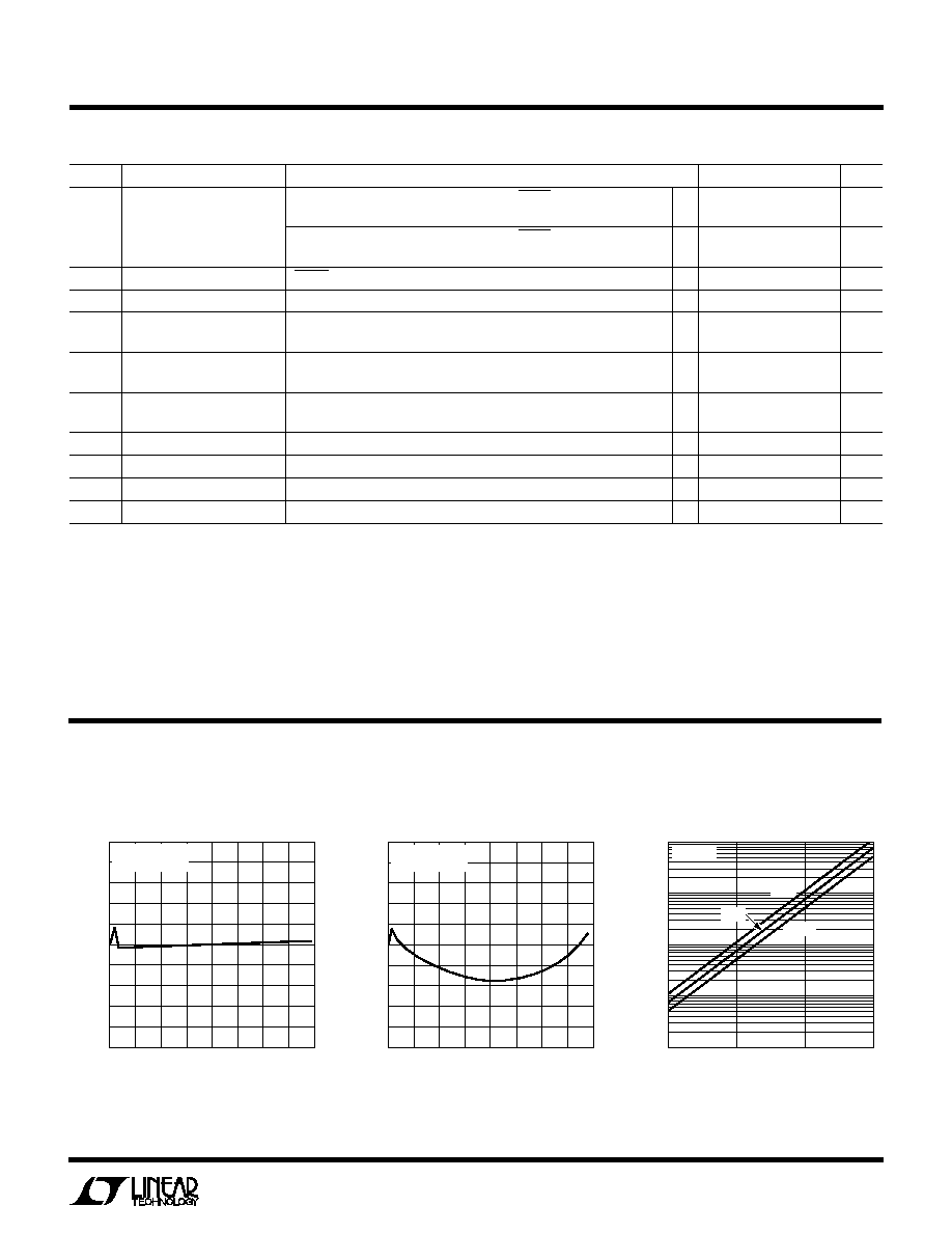
CODE
0
0.05
DNL ERROR (LSB)
0.04
0.02
0.01
0
0.05
0.02
16
32
40
1426 G01
0.03
0.03
0.04
0.01
8
24
48
56
64
V
CC
= V
REF
= 5V
T
A
= 25
°
C
CODE
0
0.05
ERROR (LSB)
0.04
0.02
0.01
0
0.05
0.02
16
32
40
1426 G02
0.03
0.03
0.04
0.01
8
24
48
56
64
V
CC
= V
REF
= 5V
T
A
= 25
°
C
OUTPUT CURRENT SINK CAPABILITY (mA)
1
OUTPUT PULL-DOWN VOLTAGE (mV)
100
1000
0.1
10
100
1426 G03
0.1
1
10
85
°
C
40
°
C
V
CC
= 5V
25
°
C
Output Pull-Down Voltage
vs Output Current Sink Capability
Integral Nonlinearity (INL)
Differential Nonlinearity (DNL)
4
LTC1426
TYPICAL PERFOR
M
A
N
CE CHARACTERISTICS
U
W
TEMPERATURE (
°
C)
40
0
CLOCK HIGH TIME (ns)
100
200
300
400
500
600
15
10
35
60
1426 G04
85
V
CC
= 3V
V
CC
= 5V
TEMPERATURE (
°
C)
40
0
SUPPLY CURRENT (
µ
A)
10
20
30
40
50
60
15
10
35
60
1426 G06
85
PUSHBUTTON
MODE
PULSE
MODE
V
CC
= 5V
Supply Current vs Temperature
LOGIC INPUT VOLTAGE (V)
0
SUPPLY CURRENT (
µ
A)
38.5
36.5
34.5
32.5
30.5
28.5
26.5
24.5
22.5
4
1426 F05
1
2
3
5
PULSE
MODE
PUSHBUTTON
MODE
T
A
= 25
°
C
CLK1 AND CLK2
TIED TOGETHER
Supply Current
vs Logic Input Voltage
PI
N
FU
N
CTIO
N
S
U
U
U
span. Bypass V
REF
to GND with an external capacitor to
minimize output errors. V
REF
can be tied to V
CC
if desired.
V
CC
(Pin 7): Voltage Supply. This supply must be kept free
from noise and ripple by bypassing directly to the ground
plane.
SHDN (Pin 8): Shutdown. A logic low puts the chip into
shutdown mode with the PWM outputs in high imped-
ance. The digital settings for the DACs are retained in
shutdown.
CLK1 (Pin 1): Channel 1 Clock/Pushbutton Input.
CLK2 (Pin 2): Channel 2 Clock/Pushbutton Input.
GND (Pin 3): Ground. It is recommended that GND be tied
to a ground plane.
PWM1 (Pin 4): Channel 1 PWM Output.
PWM2 (Pin 5): Channel 2 PWM Output.
V
REF
(Pin 6): Voltage Reference Input. V
REF
powers the
DAC output buffers and can be used to control the output
CLK1
CLK2
t
CKL0
1426 TC01
t
CKHI
1426 TC02
CLK1
CLK2
t
PW
Pushbutton Mode Timing
Pulse Mode Timing
TI I G DIAGRA S
W
W
U
Minimum Clock High Time
vs Temperature
5
LTC1426
BLOCK DIAGRA
M
W
APPLICATIO
N
S I
N
FOR
M
ATIO
N
W
U
U
U
PWM1
V
REF
PWM2
1426 F01
COMPARATOR
COMPARATOR
DRIVER
DRIVER
6-BIT
UP/DOWN
COUNTER
DEBOUNCE
CIRCUIT
6-BIT
UP
COUNTER
LATCH
AND
LOGIC
CONTROL
LOGIC
MODE SELECT
0 = PUSHBUTTON MODE
1 = PULSE MODE
6-BIT
UP/DOWN
COUNTER
6
6
6
POWER-ON
RESET
OSCILLATOR
SHDN
INPUT
CONDITIONING
CLK1
CLK2
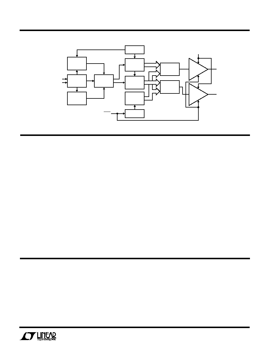
Figure 1. LTC1426 Block Diagram
DEFI ITIO S
U
U
LSB: The least significant bit or the ideal duty cycle
difference between two successive codes.
LSB = DC
MAX
/64
DC
MAX
= The DAC output maximum duty cycle
Resolution: The resolution is the number of DAC output
states (64) that divide the full-scale output duty cycle
range. The resolution does not necessarily imply linearity.
INL: End point integral nonlinearity is the maximum devia-
tion from a straight line passing through the end points of
the DAC transfer curve. The INL error at a given code is
calculated as follows:
INL = (DC
OUT
DC
IDEAL
)/LSB
DC
IDEAL
= (Code)(LSB)
DC
OUT
= the DAC output duty cycle measured at the
given number of clocked in pulses.
DNL: Differential nonlinearity is the difference between the
measured duty cycle change and the ideal 1LSB duty cycle
change between any two adjacent codes. The DNL error
between any two codes is calculated as follows:
DNL = (
DC
OUT
LSB)/LSB
DC
OUT
= The measured duty cycle difference between
two adjacent codes.
Full-Scale Error: Full-scale error is the difference between
the ideal and measured DAC output duty cycles with all bits
set to one (Code = 63). The full-scale error is calculated as
follows:
FSE = (DC
OUT
DC
IDEAL
)/LSB
DC
IDEAL
= DC
MAX
Dual 6-Bit PWM DAC
Figure 1 shows a block diagram of the LTC1426. Each
6-bit PWM DAC is guaranteed monotonic and is digitally
adjustable in 64 equal steps, which corresponds from 0%
to 98.5% duty cycle full scale. At power-up, the counters
reset to 100000B and both DAC outputs assume midscale
duty cycle. The PWM outputs have an output impedance
of less than 100
. The DAC outputs swing from 0V to the
reference voltage, V
REF
, which can be biased from 0V to
5.5V. The frequency of the DAC outputs is above 3kHz,
easing output filtering.
In the case of a pure resistive load, the voltage measured
across load RL is given by:
V = (V
PWM
)R
L
/(R
L
+ R
OUT
)