Äîêóìåíòàöèÿ è îïèñàíèÿ www.docs.chipfind.ru
1
LTC1382
5V Low Power
RS232 Transceiver
with Shutdown
S
FEATURE
D
U
ESCRIPTIO
s
Operates from a Single 5V Supply
s
Low Supply Current: I
CC
= 220
µ
A
s
I
CC
= 0.2
µ
A in Shutdown Mode
s
ESD Protection Over
±
10kV
s
Uses Small Capacitors: 0.1
µ
F
s
Operates to 120kBaud
s
Output Overvoltage Does Not Force Current
Back into Supplies
s
RS232 I/O Lines Can Be Forced to
±
25V
Without Damage
s
Pin Compatible with LT1180A
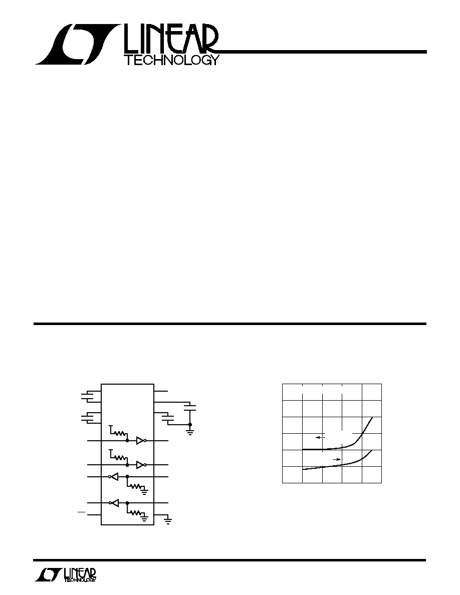
The LTC1382 is an ultra-low power 2-driver/2-receiver
RS232 transceiver that operates from a single 5V
supply. The charge pump requires only four space-
saving 0.1
µ
F capacitors.
The transceiver operates in one of two modes, Normal
and Shutdown. In the Normal mode, I
CC
is only 220
µ
A
with the driver outputs unloaded. In the Shutdown
mode, the charge pump is turned off, the driver outputs
are forced into three-state, both receivers are off and
I
CC
drops to 0.2
µ
A.
The LTC1382 is fully compliant with all data rate and
overvoltage RS232 specifications. The transceiver can
operate up to 120kbaud with a 2500pF, 3k
load. Both
driver outputs and receiver inputs can be forced to
±
25V without damage and can survive multiple
±
10kV
ESD strikes.
U
S
A
O
PPLICATI
s
Notebook Computers
s
Palmtop Computers
U
A
O
PPLICATI
TYPICAL
TEMPERATURE (°C)
20
0
QUIESCENT CURRENT (
µ
A)
100
200
300
400
600
0
20
40
60
LTC1382 · TA02
80
500
TEST CONDITION: V
CC
= 5V
0
SHUTDOWN CURRENT (
µ
A)
0.2
0.4
0.6
0.8
1.2
1.0
QUIESCENT
CURRENT
SHUTDOWN
CURRENT
Quiescent and Shutdown Supply Current
vs Temperature
2-Drivers/2-Receivers with Shutdown
LTC1382 · TA01
LTC1382
2
4
0.1
µ
F
17
V
CC
= 5V
3
0.1
µ
F
7
0.1
µ
F
0.1
µ
F
5
6
232 OUTPUT
15
8
232 OUTPUT
300k
14
232 INPUT
5k
9
232 INPUT
16
12
11
13
10
LOGIC INPUT
LOGIC INPUT
LOGIC OUTPUT
LOGIC OUTPUT
300k
5k
18
ON/OFF
V
CC
V
CC
2
LTC1382
A
U
G
W
A
W
U
W
A
R
BSOLUTE
XI
TI
S
W
U
U
PACKAGE/ORDER I FOR ATIO
Supply Voltage (V
CC
) ................................................ 6V
Input Voltage
Driver ....................................... 0.3V to V
CC
+ 0.3V
Receiver ............................................... 25V to 25V
Digital Input ............................... 0.3V to V
CC
+ 0.3V
Output Voltage
Driver .................................................... 25V to 25V
Receiver .................................... 0.3V to V
CC
+ 0.3V
Short-Circuit Duration
V
+
................................................................... 30 sec
V
................................................................... 30 sec
Driver Output .............................................. Indefinite
Receiver Output .......................................... Indefinite
Operating Temperature Range .................... 0
°
C to 70
°
C
Storage Temperature Range ................ 65
°
C to 150
°
C
Lead Temperature (Soldering, 10 sec)................. 300
°
C
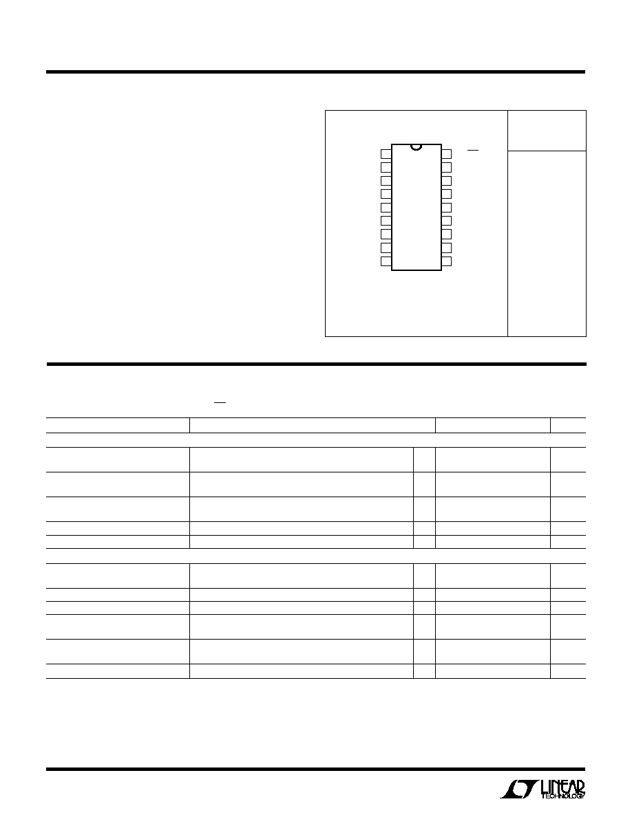
ORDER PART
NUMBER
LTC1382CN
LTC1382CS
ELECTRICAL C
C
HARA TERISTICS
C
D
T
JMAX
= 125
°
C,
JA
= 56
°
C/W (N)
T
JMAX
= 125
°
C,
JA
= 85
°
C/W (S)
1
2
3
4
5
6
7
8
9
TOP VIEW
S PACKAGE
18-LEAD PLASTIC SOL
18
17
16
15
14
13
12
11
10
NC
C1
+
V
+
C1
C2
+
C2
V
TR2 OUT
RX2 IN
ON/OFF
V
CC
GND
TR1 OUT
RX1 IN
RX1 OUT
TR1 IN
TR2 IN
RX2 OUT
N PACKAGE
18-LEAD PLASTIC DIP
Consult factory for Industrial and Military grade parts.
V
CC
= 5V, C1 = C2 = C3 = C4 = 0.1
µ
F, V
ON/OFF
= V
CC
unless otherwise noted.
PARAMETER
CONDITIONS
MIN
TYP
MAX
UNITS
Any Driver
Output Voltage Swing
3k to GND
Positive
q
5.0
7.0
V
Negative
q
5.0
6.5
V
Logic Input Voltage Level
Input Low Level (V
OUT
= High)
q
1.4
0.8
V
Input High Level (V
OUT
= Low)
q
2.0
1.4
V
Logic Input Current
V
IN
= V
CC
q
5
µ
A
V
IN
= 0V
q
20
40
µ
A
Output Short-Circuit Current
V
OUT
= 0V
±
12
mA
Output Leakage Current
Shutdown or V
CC
= 0V (Note 3), V
OUT
=
±
20V
q
±
10
±
500
µ
A
Any Receiver
Input Voltage Thresholds
Input Low Threshold
q
0.8
1.3
V
Input High Threshold
q
1.7
2.4
V
Hysteresis
q
0.1
0.4
1
V
Input Resistance
10V
V
IN
10V
3
5
7
k
Output Voltage
Output Low, I
OUT
= 1.6mA (V
CC
= 5V)
q
0.2
0.4
V
Output High, I
OUT
= 160
µ
A (V
CC
= 5V)
q
3.0
3.2
V
Output Short-Circuit Current
Sinking Current, V
OUT
= V
CC
15
40
mA
Sourcing Current V
OUT
= 0V
10
20
mA
Output Leakage Current
Shutdown (Note 3), 0V
V
OUT
V
CC
q
1
10
µ
A
3
LTC1382
ELECTRICAL C
C
HARA TERISTICS
C
D
V
CC
= 5V, C1 = C2 = C3 = C4 = 0.1
µ
F, V
ON/OFF
= V
CC
, unless otherwise noted.
C
C
HARA TERISTICS
AC
PARAMETER
CONDITIONS
MIN
TYP
MAX
UNITS
Power Supply Generator
V
+
Output Voltage
I
OUT
= 0mA
8.0
V
I
OUT
= 8mA
7.5
V
V
Output Voltage
I
OUT
= 0mA
8.0
V
I
OUT
= 8mA
7.0
V
Supply Rise Time
Shutdown to Turn-On
0.2
ms
Power Supply
V
CC
Supply Current
No Load (Note 2)
q
0.22
0.5
mA
Supply Leakage Current (V
CC
)
Shutdown (Note 3)
q
0.2
10
µ
A
Digital Input Threshold Low
q
1.4
0.8
V
Digital Input Threshold High
q
2.0
1.4
V
V
CC
= 5V, C1 = C2 = C3 = C4 = 0.1
µ
F, unless otherwise noted.
The
q
denotes specifications which apply over the operating temperature
range of 0
°
C
T
A
70
°
C.
Note 1: Absolute maximum ratings are those values beyond which the life
of the device may be impaired.
Note 2: Supply current is measured with driver and receiver outputs
unloaded.
Note 3: Measurements made in the Shutdown mode are performed
with V
ON/OFF
= 0V.
PARAMETER
CONDITIONS
MIN
TYP
MAX
UNITS
Slew Rate
R
L
= 3k, C
L
= 51pF
8
30
V/
µ
s
R
L
= 3k, C
L
= 2500pF
3
5
V/
µ
s
Driver Propagation Delay
t
HLD
(Figure 1)
q
2
3.5
µ
s
(TTL to RS232)
t
LHD
(Figure 1)
q
2
3.5
µ
s
Receiver Propagation Delay
t
HLR
(Figure 2)
q
0.3
0.8
µ
s
(RS232 to TTL)
t
LHR
(Figure 2)
q
0.3
0.8
µ
s
TYPICAL PERFOR
M
A
N
CE CHARACTERISTICS
U
W
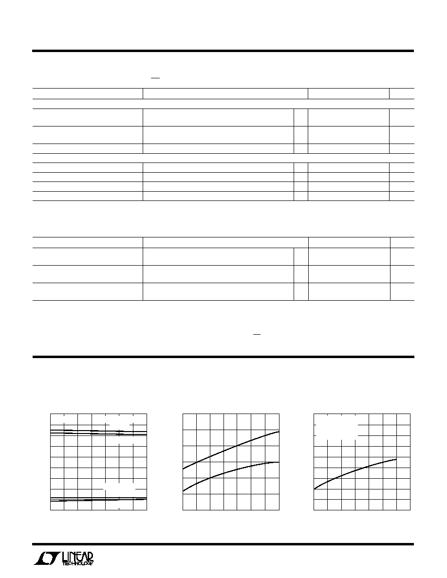
Driver Output Voltage
vs Temperature
TEMPERATURE (°C)
0
8
DRIVER OUTPUT VOLTAGE (V)
6
2
0
2
40
10
LTC1382 · TPC01
4
20
10
50
60
30
70
4
6
8
R
L
= 3k
V
CC
= 5V
V
CC
= 4.5V
OUTPUT HIGH
V
CC
= 4.5V
V
CC
= 5V
OUTPUT LOW
DATA RATE (kBAUD)
0
0
SUPPLY CURRENT (mA)
5
15
20
25
100
45
LTC1382 · TPC03
10
50
25
125
75
150
175
30
35
40
V
CC
= 5V
R
L
= 3k
C
L
= 2500pF
2 DRIVERS ACTIVE
TEMPERATURE (°C)
0
THRESHOLD VOLTAGE (V)
1.8
2.0
2.2
30
50
V
TH
V
TL
LTC1382 · TPC02
1.6
1.4
10
20
40
60
70
1.2
1.0
Receiver Input Thresholds
vs Temperature
Supply Current vs Data Rate
4
LTC1382
TYPICAL PERFOR
M
A
N
CE CHARACTERISTICS
U
W
TEMPERATURE (°C)
0
0
SUPPLY CURRENT (mA)
2
6
8
10
40
18
LTC1382 · TPC04
4
20
10
50
30
60
70
12
14
16
2 DRIVERS LOADED
R
L
= 3k
1 DRIVER LOADED
R
L
= 3k
V
CC
Supply Current
vs Temperature
Receiver Short-Circuit Current
vs Temperature
TEMPERATURE (°C)
0
10
SHORT-CIRCUIT CURRENT (mA)
30
20
40
LTC1382 · TPC06
20
10
I
SC
+
I
SC
50
30
60
70
40
50
Driver Short-Circuit Current
vs Temperature
TEMPERATURE (°C)
0
0
SHORT-CIRCUIT CURRENT (mA)
2
6
8
10
40
18
LTC1382 · TPC05
4
20
10
50
30
60
70
12
14
16
I
SC
I
SC
+
Driver Leakage in Shutdown
vs Temperature
TEMPERATURE (°C)
0
LEAKAGE CURRENT (
µ
A)
60
45
40
35
30
25
20
15
10
5
0
LTC1349 · TPC05
20
70
10
30
40
50
V
OUT
= 20V
V
OUT
= 20V
Driver Output Waveforms
Receiver Output Waveforms
INPUT
INPUT
LTC1382 · TPC08
LTC1382 · TPC09
RECEIVER
OUTPUT
C
L
= 51pF
DRIVER
OUTPUT
R
L
= 3k
C
L
= 2500pF
DRIVER
OUTPUT
R
L
= 3k
5
LTC1382
PI FU CTIO S
U
U
U
V
CC
: 5V Input Supply Pin. This pin should be decoupled
with a 0.1
µ
F ceramic capacitor.
GND: Ground Pin.
ON/OFF: TTL/CMOS Compatible Shutdown Pin. A logic
low puts the device in the Shutdown mode. Both driver
outputs are forced into three-state and the supply current
is 0.2
µ
A.
V
+
: Positive Supply Output (RS232 Drivers). V
+
2V
CC
2V. This pin requires an external capacitor C = 0.1
µ
F for
charge storage. The capacitor may be tied to ground or
V
CC
. With multiple devices, the V
+
and V
pins may share
a common capacitor. For large numbers of devices, in-
creasing the size of the shared common storage capaci-
tors is recommended to reduce ripple.
V
: Negative Supply Output (RS232 Drivers). V
(2V
CC
2V). This pin requires an external capacitor C = 0.1
µ
F for
charge storage.
C1
+
, C1
, C2
+
, C2
: Commutating Capacitor Inputs. These
pins require two external capacitors C = 0.1
µ
F: one from
C1
+
to C1
and another from C2
+
to C2
. To maintain
charge pump efficiency, the capacitor's effective series
resistance should be less than 2
.
TR IN: RS232 Driver Input Pins. Inputs are TTL/CMOS
compatible. The inputs of unused drivers can be left
unconnected since 300k input pull-up resistors to V
CC
are
included on chip. To minimize power consumption, the
internal driver pull-up resistors are disconnected from V
CC
in the Shutdown mode.
TR OUT: Driver Outputs at RS232 Voltage Levels. Outputs
are in a high impedance state when in the Shutdown or
V
CC
= 0V. The driver outputs are protected against ESD to
±
10kV for human body model discharges.
RX IN: Receiver Inputs. These pins can be forced to
±
25V
without damage. The receiver inputs are protected against
ESD to
±
10kV for human body model discharges. Each
receiver provides 0.4V of hysteresis for noise immunity.
RX OUT: Receiver Outputs with TTL/CMOS Voltage Lev-
els. Outputs are in a high impedance state when in the
Shutdown mode.
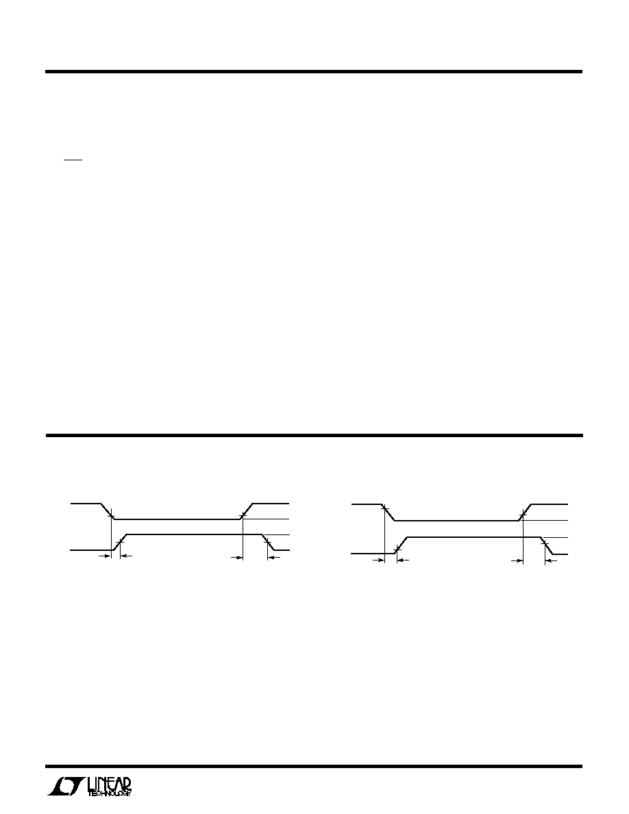
Figure 1. Driver Propagation Delay Timing
Figure 2. Receiver Propagation Delay Timing
SWITCHI G TI E WAVEFOR S
W
W
U
1.4V
0V
V
CC
0V
V
+
V
0V
DRIVER
INPUT
DRIVER
OUTPUT
1.4V
t
HLD
t
LHD
LTC1382 · F01
0.8V
V
CC
0V
2.4V
RX
INPUT
RX
OUTPUT
1.3V
t
HLR
1.7V
t
LHR
LTC1382 · F02
V
CC
0V