Äîêóìåíòàöèÿ è îïèñàíèÿ www.docs.chipfind.ru
1
LTC1324
Single Supply LocalTalk
®
Transceiver
s
Single Chip 5V LocalTalk Port
s
Low Power: I
CC
= 1mA Typ
s
Shutdown Pin Reduces I
CC
to 1
µ
A Typ
s
Digitally Selectable Low Slew Rate Mode for
Reduced EMI Emmisions
s
Drivers Maintain High Impedance in Three-State or
with Power Off
s
Thermal Shutdown Protection
s
Drivers Are Short-Circuit Protected
The LTC
®
1324 is a single 5V line transceiver designed to
operate on Apple
®
LocalTalk networks. The driver features
a digitally selectable low slew rate mode for reduced EMI
emissions. The chip draws only 1mA quiescent current
when active and 1
µ
A in shutdown. The differential driver
outputs three-state when disabled, during shutdown or
when the power is off. The driver outputs will maintain
high impedance even with output common mode voltages
beyond the power supply rails. Both the driver outputs and
receiver inputs are protected against ESD damage to
±
10kV.
The LTC1324 is available in a 16-pin SO Wide package.
FEATURES
DESCRIPTIO
N
U
s
LocalTalk Peripherals
s
Notebook and Palmtop Computers
s
Battery-Powered Systems
APPLICATIO
N
S
U
, LTC and LT are registered trademarks of Linear Technology Corporation.
Apple and LocalTalk are registered trademarks of Apple Computer, Inc.
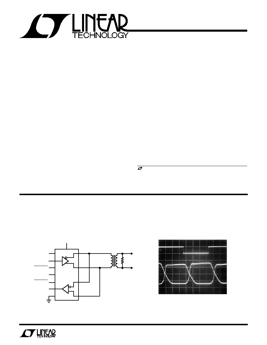
TYPICAL APPLICATIO
N
U
Waveform of Driver
Typical LocalTalk Connection for Low EMI
2
3
4
5
6
7
8
12
16
5V
LocalTalk
TRANSFORMER
11
10
9
LTC1324
SLEW RATE CONTROL
DATA IN
TX ENABLE
SHUTDOWN
RX ENABLE
DATA OUT
1324 TA01
120
TIME (0.5
µ
s/DIV)
1324 TA02
D
IN
5V/DIV
D
OUT
1V/DIV
2
LTC1324
ABSOLUTE
M
AXI
M
U
M
RATINGS
W
W
W
U
(Note 1)
Supply Voltage (V
CC
) ................................................ 7V
Input Voltage (Logic Inputs) ........ 0.3V to (V
CC
+ 0.3V)
Input Voltage (Receiver Inputs) ............................
±
1 5V
Driver Output Voltage (Forced) .............................
±
15V
Driver Short-Circuit Duration .......................... Indefinite
Operating Temperature Range .................... 0
°
C to 70
°
C
Storage Temperature Range ................. 65
°
C to 150
°
C
Lead Temperature (Soldering, 10 sec).................. 300
°
C
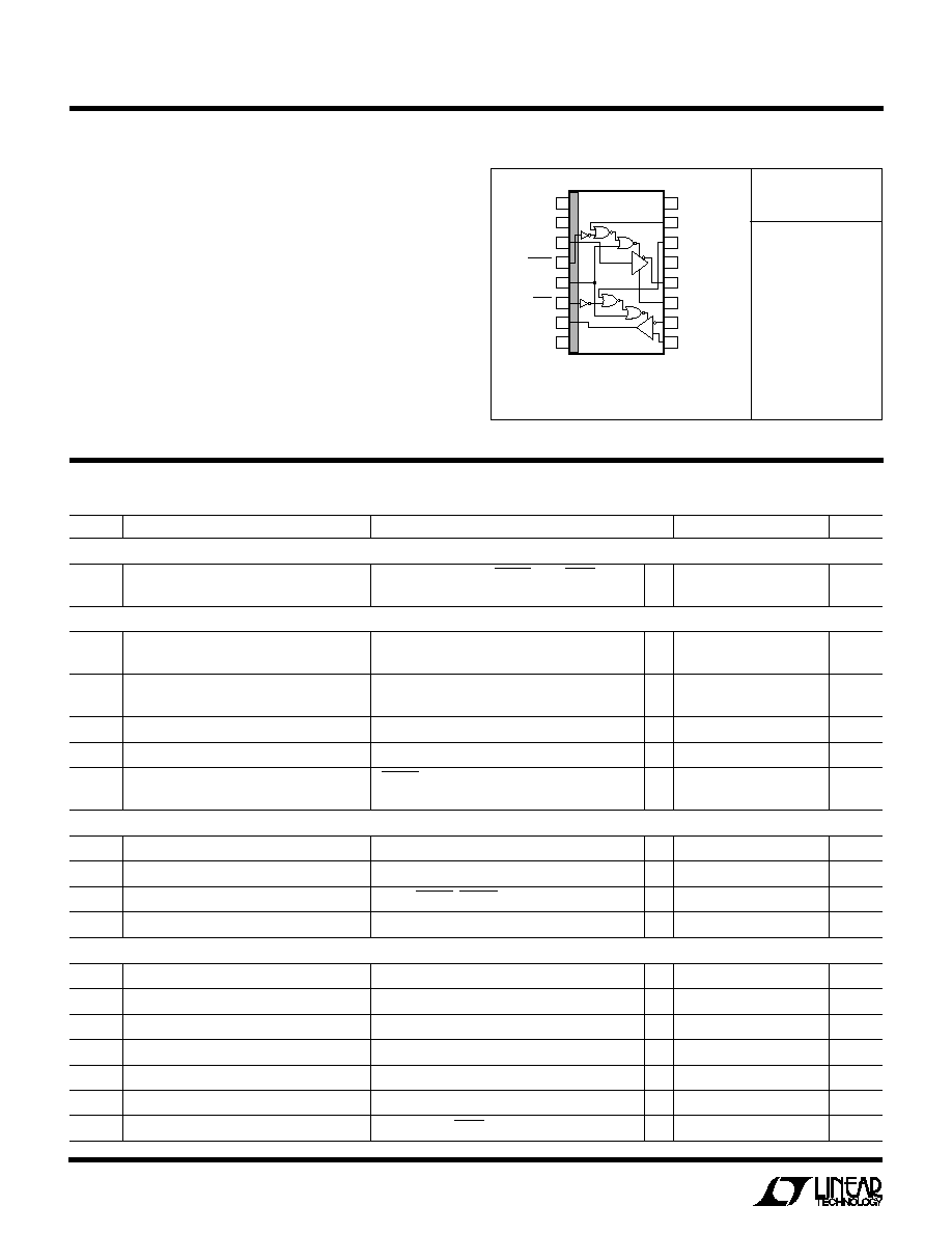
PACKAGE/ORDER I
N
FOR
M
ATIO
N
W
U
U
ORDER PART
NUMBER
LTC1324CN
LTC1324CSW
1
2
3
4
5
6
7
8
TOP VIEW
N PACKAGE
16-LEAD PDIP
16
15
14
13
12
11
10
9
NC
SR
TXD
TXDEN
SHDN
RXEN
RXO
GND
V
CC
TXDEN
RXEN
NC
TXD
TXD
+
RXD
RXD
+
DX
RX
SW PACKAGE
16-LEAD PLASTIC SO WIDE
T
JMAX
= 150
°
C,
JA
= 110
°
C/ W (N)
T
JMAX
= 150
°
C,
JA
= 150
°
C/ W (SW)
Consult factory for Industrial and Military grade parts.
V
CC
= 5V, T
A
= 0
°
C to 70
°
C (Notes 2, 3), unless otherwise noted.
ELECTRICAL CHARACTERISTICS
SYMBOL
PARAMETER
CONDITIONS
MIN
TYP
MAX
UNITS
Supplies
I
CC
Normal Operation Supply Current
No Load, SHDN = 0V, TXDEN = 0V, RXEN = 0V
q
1
2
mA
Shutdown Supply Current
No Load, SHDN = V
CC
q
1
10
µ
A
Differential Driver
V
OD
Differential Output Voltage
No Load
q
±
4.0
V
R
L
= 50
(Figure 1)
q
±
2.0
V
V
OD
Change in Magnitude of Differential
R
L
= 50
(Figure 1)
0.2
V
Output Voltage
V
OC
Differential Common Mode Output Voltage
R
L
= 50
(Figure 1)
3.0
V
I
SS
Short-Circuit Current
0V
V
O
5V
q
35
120
250
mA
I
OZ
Three-State Output Current
(TXDEN = V
CC
and TXDEN = GND) or
q
±
2
±
200
µ
A
SHDN = V
CC
or Power Off, 10V
V
O
10V
Logic Inputs
V
IH
Input High Voltage
All Logic Input Pins
q
2.4
V
V
IL
Input Low Voltage
All Logic Input Pins
q
0.8
V
I
IN
Input Current
SHDN, TXDEN, RXDEN, V = 0V to V
CC
q
±
1
±
20
µ
A
I
DN
Pull-Down Current
RXDEN, TXDEN, SR, V = 0V to V
CC
q
15
60
µ
A
Receiver
R
IN
Input Resistance
7V
V
IN
7V
12
k
Receiver Threshold Voltage
7V
V
CM
7V
q
200
200
mV
Receiver Input Hysteresis
7V
V
CM
7V
70
mV
V
OH
Output High Voltage
I
O
= 4mA
q
3.5
V
V
OL
Output Low Voltage
I
O
= 4mA
q
0.4
V
I
SS
Output Short-Circuit Current
0V
V
O
5V
q
7
85
mA
I
OZ
Output Three-State Current
0V
V
O
5V, RXEN = V
CC
, RXEN = GND
q
±
2
±
100
µ
A
3
LTC1324
V
CC
= 5V, T
A
= 0
°
C to 70
°
C (Notes 2, 3), unless otherwise noted.
ELECTRICAL CHARACTERISTICS
SYMBOL
PARAMETER
CONDITIONS
MIN
TYP
MAX
UNITS
Switching Characteristics
t
PLH
, t
PHL
Driver Propagation Delay
R
L
= 100
, C
L
= 100pF (Figures 2, 4)
q
40
120
ns
Without Slew Rate Control
SR = GND
Driver Propagation Delay
R
L
= 100
, C
L
= 100pF (Figures 2, 4)
q
0.4
1.2
µ
s
with Slew Rate Control
SR = V
CC
Receiver Propagation Delay
C
L
= 15pF (Figures 2, 6)
q
40
120
ns
t
SKEW
Driver Output to Output
R
L
= 100
, C
L
= 100pF (Figures 2, 4)
q
10
35
ns
Without Slew Rate Control
SR = GND
Driver Output to Output
R
L
= 100
, C
L
= 100pF (Figures 2, 4)
q
25
100
ns
with Slew Rate Control
SR = V
CC
t
r
, t
f
Driver Rise/Fall Time
R
L
= 100
, C
L
= 100pF (Figures 2,4)
q
20
50
ns
Without Slew Rate Control
SR = GND
Driver Rise/Fall Time
R
L
= 100
, C
L
= 100pF (Figures 2, 4)
q
0.4
1.2
µ
s
with Slew Rate Control
SR = V
CC
t
Hdis
, t
Ldis
Driver Output Active to Disable
C
L
= 15pF (Figures 3, 5)
q
50
150
ns
Without Slew Rate Control
SR = GND
Driver Output Active to Disable
C
L
= 15pF (Figures 3, 5)
q
0.7
2
µ
s
with Slew Rate Control
SR = V
CC
Receiver Output Active to Disable
C
L
= 15pF (Figures 3, 7)
q
30
100
ns
t
ENH
, t
ENL
Driver Enable to Output Active
C
L
= 15pF (Figures 3, 5)
q
50
150
ns
Without Slew Rate Control
SR = GND
Driver Enable to Output Active
C
L
= 15pF (Figures 3, 5)
q
250
750
ns
with Slew Rate Control
SR = V
CC
Receiver Enable to Output Active
C
L
= 15pF (Figures 3, 7)
q
30
100
ns
The
q
denotes specifications which apply over the full operating
temperature range.
Note 1: Absolute Maximum Ratings are those values beyond which the life
of a device may be impaired.
Note 2: All currents into device pins are positive and all currents out of
device pins are negative. All voltages are reference to ground unless
otherwise specified.
Note 3: All typicals are given at V
CC
= 5V, T
A
= 25
°
C.
TYPICAL PERFOR
M
A
N
CE CHARACTERISTICS
U
W
DRIVER DIFFERENTIAL OUTPUT VOLTAGE (V)
0
0.5
1.5
2.5
3.5
OUTPUT CURRENT (mA)
4.0
1324 G01
1.0
2.0
3.0
80
70
60
50
40
30
20
10
0
T
A
= 25
°
C
Driver Differential Output Voltage
vs Output Current
Driver Output Low Voltage
vs Output Current
OUTPUT VOLTAGE (V)
0
OUTPUT CURRENT (mA)
120
100
80
60
40
20
0
0.5
1.0
1.5
2.0
1324 G02
2.5
3.0
T
A
= 25
°
C
DRIVER OUTPUT HIGH VOLTAGE (V)
1.0
OUTPUT CURRENT (mA)
4.0
1324 G03
2.0
3.0
5.0
105
90
75
60
45
30
15
0
1.5
2.5
3.5
4.5
T
A
= 25
°
C
Driver Output High Voltage
vs Output Current
4
LTC1324
TYPICAL PERFOR
M
A
N
CE CHARACTERISTICS
U
W
TEMPERATURE (
°
C)
55
OUTPUT CURRENT (mA)
65
19
18
17
16
15
14
13
12
11
10
1324 G07
35
125
15
5
25
45
85 105
Driver Short-Circuit Current
vs Temperature
TEMPERATURE (
°
C)
55
TIME (ns)
65
4.2
4.0
3.8
3.6
3.4
3.2
3.0
1324 G09
35
125
15
5
25
45
85 105
Supply Current (Driver and
Receiver Enabled) vs Temperature
TEMPERATURE (
°
C)
55
OUTPUT CURRENT (mA)
65
110
100
90
80
70
60
50
40
1324 G06
35
125
15
5
25
45
85 105
OUTPUT VOLTAGE (V)
2.0
2.5
OUTPUT CURRENT (mA)
3.0
4.0
3.5
4.5
5.0
1324 G05
16
14
12
10
8
6
4
2
0
T
A
= 25
°
C
Receiver Output High Voltage
vs Output Current
Receiver Output Low Voltage
vs Output Current
OUTPUT VOLTAGE (V)
0
OUTPUT CURRENT (mA)
30
25
20
15
10
5
0
0.4
0.8
1.2
1.6
1324 G04
2.0
T
A
= 25
°
C
Receiver Short-Circuit Current
vs Temperature
TEMPERATURE (
°
C)
55
SUPPLY CURRENT (
µ
A)
65
900
875
850
825
800
775
750
725
700
1324 G08
35
125
15
5
25
45
85 105
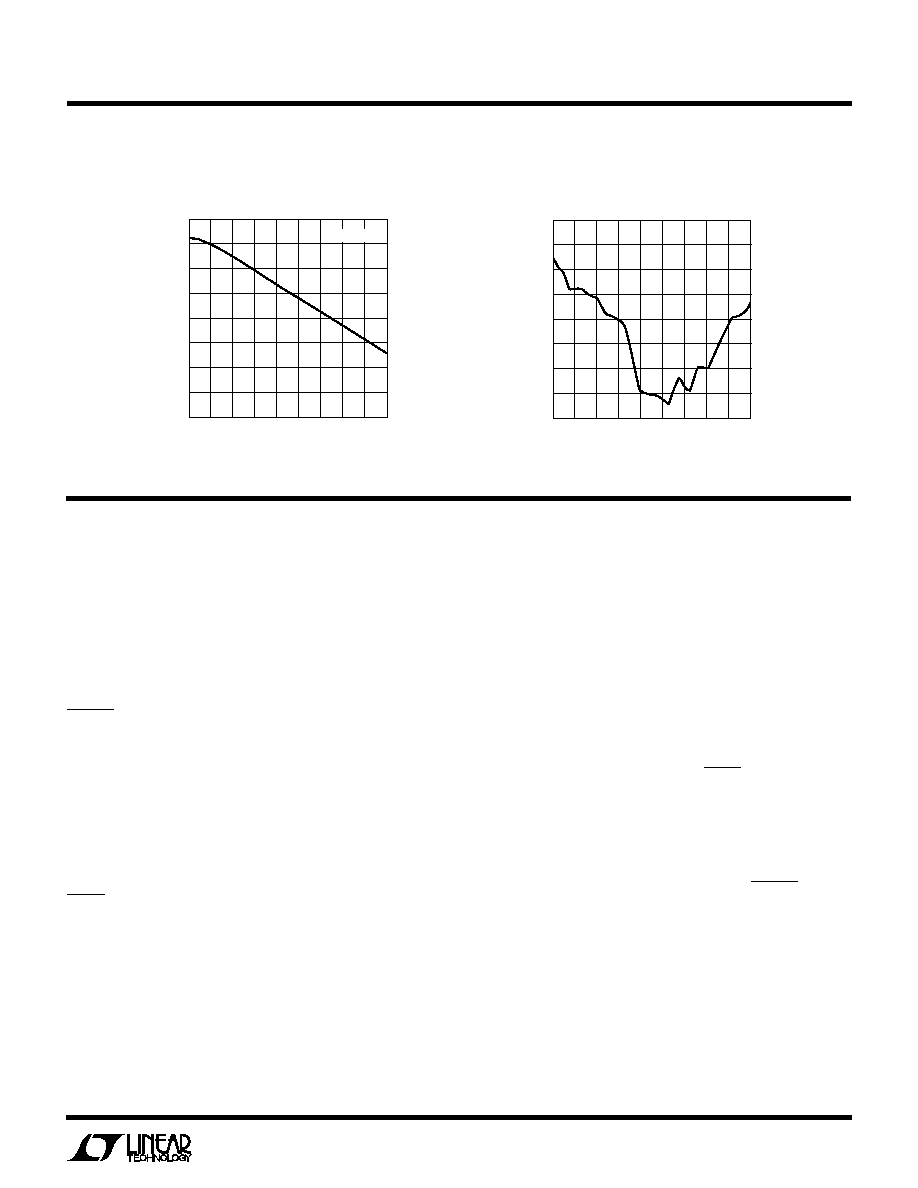
Driver Skew vs Temperature
Receiver Output Low Voltage
vs Temperature
TEMPERATURE (
°
C)
55
OUTPUT VOLTAGE (V)
65
0.8
0.7
0.6
0.5
0.4
0.3
0.2
0.1
0
1324 G10
35
125
15
5
25
45
85 105
I = 8mA
Receiver Output High Voltage
vs Temperature
TEMPERATURE (
°
C)
55
OUTPUT VOLTAGE (V)
65
4.00
3.75
3.50
3.25
3.00
2.75
2.50
2.25
2.00
1324 G11
35
125
15
5
25
45
85 105
I = 8mA
5
LTC1324
TYPICAL PERFOR
M
A
N
CE CHARACTERISTICS
U
W
Receiver
t
PLH
t
PHL
vs Temperature
TEMPERATURE (
°
C)
55
TIME (ns)
65
8
7
6
5
4
3
2
1
0
1324 G13
35
125
15
5
25
45
85 105
TEMPERATURE (
°
C)
55
DIFFERENTIAL VOLTAGE (V)
65
3.1
3.0
2.9
2.8
2.7
2.6
2.5
2.4
2.3
1324 G12
35
125
15
5
25
45
85 105
R
L
= 100
Driver Differential Output Voltage
vs Temperature
PI
N
FU
N
CTIO
N
S
U
U
U
GND (Pin 8): Ground.
RXD
+
(Pin 9): RS485 Receiver Noninverting Input. When
this pin is
200mV above RXD
, RXDO will be high. When
this pin is
200mV below RXD
, RXDO will be low.
RXD
(Pin 10): RS485 Receiver Inverting Input.
TXD
+
(Pin 11): RS485 Driver Noninverting Output.
TXD
(Pin 12): RS485 Driver Inverting Output.
RXEN (Pin 14): Receiver Enable (TTL Compatible). A low
level on this pin and a high level on RXEN (Pin 6) disables
the receiver and three-states the logic outputs. A high level
allows normal operation. Connected to an internal pull-
down.
TXDEN (Pin 15): Driver Output Enable (TTL Compatible).
A low level on this pin and a high level on TXDEN (Pin 4)
forces the RS485 driver into three-state. A high level
enables the driver. Connected to an internal pull-down.
V
CC
(Pin 16): The Positive Supply Input. 4.75V
V
CC
5.25V. Requires a 1
µ
F bypass capacitor to ground.
NC (Pins 1, 13): No Internal Connection.
SR (Pin 2): Slew Rate Control (TTL Compatible). A high
level on this pin forces the RS485 driver into the low slew
rate mode. A low level forces the driver into the high slew
rate or normal mode. Connected to an internal pull-down.
TXD (Pin 3): RS485 Driver Input (TTL Compatible).
TXDEN (Pin 4): Driver Output Enable (TTL Compatible). A
high level on this pin and a low level on TXDEN (Pin 15)
forces the RS485 driver into three-state. A low level
enables the driver.
SHDN (Pin 5): Shutdown Input (TTL Compatible). When
this pin is high, the chip is shut down; the driver and
receiver outputs three-state; and the supply current drops
to 1
µ
A. A low level on this pin allows normal operation.
RXEN (Pin 6): Receiver Enable (TTL Compatible). A high
level on this pin and a low level on RXEN (Pin 14) disables
the receiver and three-states the logic outputs. A low level
allows normal operation.
RXDO (Pin 7): RS485 Receiver Output.