Äîêóìåíòàöèÿ è îïèñàíèÿ www.docs.chipfind.ru
1
LTC1323
Single 5V
AppleTalk
®
Transceiver
DX
CHARGE PUMP
DX
RX
RX
RX
0.33
µ
F
CPEN
TXD
TXI
TXDEN
SHDN
RXEN
RXO
RXO
RXDO
3
2
1
4
5
6
7
8
9
10
11
12
TXD
TXD
+
TXO
RXI
RXI
RXD
+
RXD
24
21
23
22
20
19
18
17
5
TO 10
=
5
TO 10
16
14
15
13
LTC1323 · TA01
0.33
µ
F
100pF
1
µ
F
1
µ
F
5V
LTC1323
8
7
6
5
4
2
1
3
EMI FILTER
EMI FILTER
EMI FILTER
EMI FILTER
EMI FILTER
EMI FILTER
EMI FILTER
EMI FILTER
+
+
S
FEATURE
D
U
ESCRIPTIO
s
Single Chip Provides Complete
LocalTalk
®
/AppleTalk Port
s
Operates From a Single 5V Supply
s
ESD Protection to
±
10kV on Receiver Inputs
and Driver Outputs
s
Low Power: I
CC
= 2.4mA Typ
s
Shutdown Pin Reduces I
CC
to 0.5
µ
A Typ
s
Receiver Keep-Alive Function: I
CC
= 65
µ
A Typ
s
Differential Driver Drives Either Differential
AppleTalk or Single-Ended EIA562 Loads
s
Drivers Maintain High Impedance in Three-State or
with Power Off
s
Thermal Shutdown Protection
s
Drivers are Short-Circuit Protected
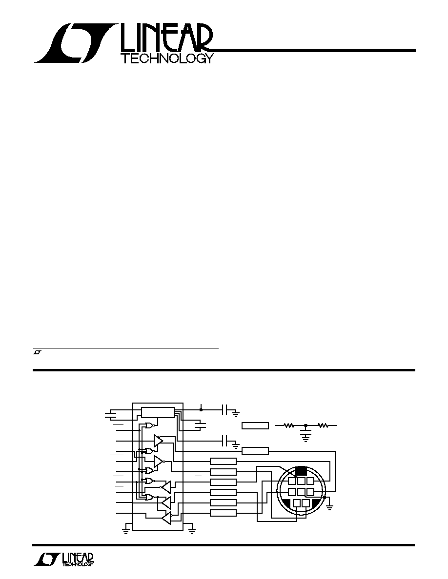
The LTC
®
1323 is a multi-protocol line transceiver designed
to operate on AppleTalk or EIA562-compatible single-
ended networks while operating from a single 5V supply.
There are two versions of the LTC1323 available: a 16-pin
version designed to connect to an AppleTalk network,
and a 24-pin version which also includes the additional
single-ended drivers and receivers necessary to create
an Apple-compatible serial port. An on-board charge
pump generates a 5V supply which can be used to
power external devices. Additionally, the 24-pin LTC1323
features a micropower keep-alive mode during which
one of the single-ended receivers is kept active to monitor
external wake-up signals. The LTC1323 draws only 2.4mA
quiescent current when active, 65
µ
A in receiver keep-
alive mode, and 0.5
µ
A in shutdown, making it ideal for
use in battery-powered systems.
The differential driver can drive either differential AppleTalk
loads or conventional single-ended loads. The driver
outputs three-state when disabled, during shutdown, in
receiver keep-alive mode, or when the power is off. The
driver outputs will maintain high impedance even with
output common-mode voltages beyond the power supply
rails. Both the driver outputs and receiver inputs are
protected against ESD damage to
±
10kV.
U
S
A
O
PPLICATI
s
LocalTalk Peripherals
s
Notebook/Palmtop Computers
s
Battery-Powered Systems
U
A
O
PPLICATI
TYPICAL
AppleTalk and LocalTalk are registered trademarks of Apple Computer, Inc.
, LTC and LT are registered trademarks of Linear Technology Corporation.
2
LTC1323
A
U
G
W
A
W
U
W
A
R
BSOLUTE
XI
TI
S
Supply Voltage (V
CC
) ................................................ 7V
Input Voltage
Logic Inputs .............................. 0.3V to V
CC
+ 0.3V
Receiver Inputs ................................................
±
15V
Driver Output Voltage (Forced) .............................
±
15V
Driver Short-Circuit Duration .......................... Indefinite
Operating Temperature Range .................... 0
°
C to 70
°
C
Storage Temperature Range ................ 65
°
C to 150
°
C
Lead Temperature (Soldering, 10 sec) ................. 300
°
C
W
U
U
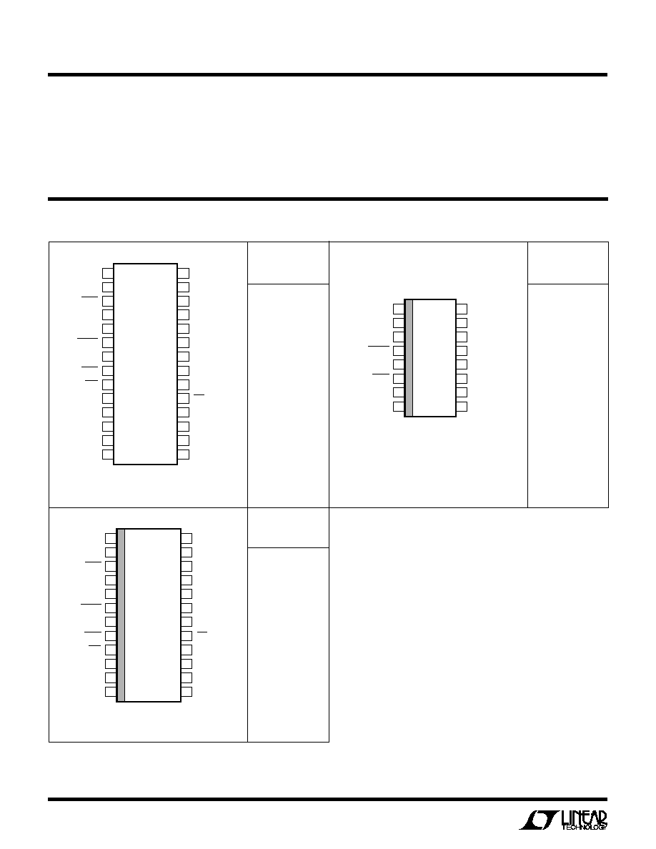
PACKAGE/ORDER I FOR ATIO
ORDER PART
NUMBER
LTC1323CS
LTC1323CG
ORDER PART
NUMBER
T
JMAX
= 150
°
C,
JA
= 96
°
C/W
ORDER PART
NUMBER
LTC1323CSW
Consult factory for Industrial and Military grade parts.
T
JMAX
= 125
°
C,
JA
= 85
°
C/W
1
2
3
4
5
6
7
8
9
10
11
12
13
14
28
27
26
25
24
23
22
21
20
19
18
17
16
15
C1
+
C2
CPEN
TXD
TXI
TXDEN
SHDN
RXEN
RXO
RXO
RXDO
NC
NC
GND
V
CC
C2
+
C2
NC
NC
V
EE
TXD
TXD
+
TXO
RXI
RXI
RXD
RXD
+
PGND
G PACKAGE
28-LEAD PLASTIC SSOP
TOP VIEW
T
JMAX
= 125
°
C,
JA
= 85
°
C/W
1
2
3
4
5
6
7
8
TOP VIEW
S PACKAGE
16-LEAD PLASTIC SO
16
15
14
13
12
11
10
9
C1
+
C1
TXD
TXDEN
SHDN
RXEN
RXDO
GND
V
CC
C2
+
C2
V
EE
TXD
TXD
+
RXD
RXD
+
1
2
3
4
5
6
7
8
9
10
11
12
TOP VIEW
SW PACKAGE
24-LEAD PLASTIC SO WIDE
24
23
22
21
20
19
18
17
16
15
14
13
C1
+
C1
CPEN
TXD
TXI
TXDEN
SHDN
RXEN
RXO
RXO
RXDO
GND
V
CC
C2
+
C2
V
EE
TXD
TXD
+
TXO
RXI
RXI
RXD
RXD
+
PGND
3
LTC1323
ELECTRICAL CHARACTERISTICS
V
CC
= 5V
±
10%, T
A
= 0
°
C to 70
°
C (Notes 2, 3)
SYMBOL
PARAMETER
CONDITIONS
MIN
TYP
MAX
UNITS
Supplies
I
CC
Normal Operation Supply Current
No Load, SHDN = 0V, CPEN = 0V, TXDEN = 0V,
q
2.4
4
mA
RXEN = 0V
Receiver Keep-Alive Supply Current
No Load, SHDN = 0V, CPEN = V
CC
, TXDEN = 0V,
q
65
100
µ
A
RXEN = 0V
Shutdown Supply Current
No Load, SHDN = V
CC
, CPEN = X, TXDEN = X,
q
0.5
10
µ
A
RXEN = 0V
V
EE
Negative Supply Output Voltage
I
LOAD
10mA (Note 4),
q
5.5
5
4.5
V
V
CC
= 5V, R
L
= 100
(Figure 1),
TXI = V
CC
, R
TXO
= 3k (Figure 5)
f
OSC
Charge Pump Oscillator Frequency
200
kHz
Differential Driver
V
OD
Differential Output Voltage
No Load
q
±
8
V
R
L
= 100
(Figure 1)
q
±
2
V
OD
Change in Magnitude of Differential
R
L
= 100
(Figure 1)
0.2
V
Output Voltage
Differential Driver
V
OC
Differential Common-Mode
R
L
= 100
3
V
Output Voltage
V
OS
Single-Ended Output Voltage
No Load
q
±
4.0
V
R
L
= 3k to GND
q
±
3.7
V
V
CMR
Common-Mode Range
SHDN = V
CC
or CPEN = V
CC
or Power Off
q
±
10
V
I
SS
Short-Circuit Current
5V
V
O
5V
q
35
120
500
mA
I
OZ
Three-State Output Current
SHDN = V
CC
or CPEN = V
CC
or Power Off,
q
±
2
±
200
µ
A
10V
V
O
10V
Single-Ended Driver (Note 5)
V
OS
Single-Ended Output Voltage
No Load
q
±
4.5
V
R
L
= 3k to GND
q
±
3.7
V
V
CMR
Common-Mode Range
SHDN = V
CC
or CPEN = V
CC
or TXDEN = V
CC
q
±
10
V
or Power Off
I
SS
Short-Circuit Current
5V
V
O
5V
q
35
220
500
mA
I
OZ
Three-State Output Current
SHDN = V
CC
or CPEN = V
CC
or TXDEN = V
CC
q
±
2
±
200
µ
A
or Power Off, 10V
V
O
10V
Receivers
R
IN
Input Resistance
7V
V
IN
7V
q
12
k
Differential Receiver Threshold Voltage
7V
V
CM
7V
q
200
200
mV
Differential Receiver Input Hysteresis
7V
V
CM
7V
q
70
mV
Single-Ended Input, Low Voltage
(Note 5)
q
0.8
V
Single-Ended Input, High Voltage
(Note 5)
q
2
V
V
OH
Output High Voltage
I
O
= 4mA
q
3.5
V
V
OL
Output Low Voltage
I
O
= 4mA
q
0.4
V
I
SS
Output Short-Circuit Current
5V
V
O
5V
q
7
85
mA
I
OZ
Output Three-State Current
5V
V
O
5V, RXEN = V
CC
q
±
2
±
100
µ
A
4
LTC1323
ELECTRICAL CHARACTERISTICS
V
CC
= 5V
±
10%, T
A
= 0
°
C to 70
°
C (Notes 2 and 3)
The
q
denotes specifications which apply over the full operating
temperature range.
Note 1: Absolute maximum ratings are those values beyond which the life
of a device may be impaired.
Note 2: All currents into device pins are positive; all currents out of device
pins are negative. All voltages are referenced to ground unless otherwise
specified.
Note 3: All typicals are given at V
CC
= 5V, T
A
= 25
°
C.
Note 4: I
LOAD
is an external current being sunk into the V
EE
pin.
Note 5: These specifications apply to the 24-pin SO Wide package only.
SYMBOL
PARAMETER
CONDITIONS
MIN
TYP
MAX
UNITS
Logic Inputs
V
IH
Input High Voltage
All Logic Input Pins
q
2.0
V
V
IL
Input Low Voltage
All Logic Input Pins
q
0.8
V
I
C
Input Current
All Logic Input Pins
q
±
1.0
±
20
µ
A
Switching Characteristics
t
PLH
, t
PHL
Differential Driver Propagation Delay
R
L
= 100
, C
L
= 100pF (Figures 2, 7)
q
40
120
ns
Differential Driver Propagation Delay
R
L
= 3k, C
L
= 100pF (Figures 3, 9)
q
120
180
ns
with Single-Ended Load
Single-Ended Driver Propagation Delay
R
L
= 3k, C
L
= 100pF, (Figures 5, 10) (Note 5)
q
40
120
ns
Differential Receiver Propagation Delay
C
L
= 15pF (Figures 2, 11)
q
70
160
ns
Single-Ended Receiver
C
L
= 15pF (Figures 6, 12) (Note 5)
q
70
160
ns
Propagation Delay
Inverting Receiver Propagation Delay
C
L
= 15pF (Figures 6, 12) (Note 5)
q
150
600
ns
in Keep-Alive Mode,
SHDN = 0V, CPEN = V
CC
t
SKEW
Differential Driver Output to Output
R
L
= 100
, C
L
= 100pF (Figures 2, 7)
q
10
50
ns
t
r
, t
f
Differential Driver Rise/Fall Time
R
L
= 100
, C
L
= 100pF (Figures 2, 7)
q
50
150
ns
Differential Driver Rise/Fall Time
R
L
= 3k, C
L
= 100pF (Figures 3, 9)
q
50
150
ns
with Single-Ended Load
Single-Ended Driver Rise/Fall Time
R
L
= 3k, C
L
= 100pF (Figures 5, 10) (Note 5)
q
15
80
ns
t
HDIS
, t
LDIS
Differential Driver Output Active
C
L
= 15pF (Figures 4, 8)
q
180
250
ns
to Disable
Any Receiver Output Active to Disable
C
L
= 15pF (Figures 4, 13)
q
30
100
ns
t
ENH
, t
ENL
Differential Driver
C
L
= 15pF (Figures 4, 8)
q
180
250
ns
Enable to Output Active
Any Receiver, Enable to Output Active
C
L
= 15pF (Figures 4, 13)
q
30
100
ns
V
EER
Supply Rise Time from Shutdown
C1 = C2 = 0.33
µ
F, C
VEE
= 1
µ
F
q
0.2
ms
or Receiver Keep-Alive
5
LTC1323
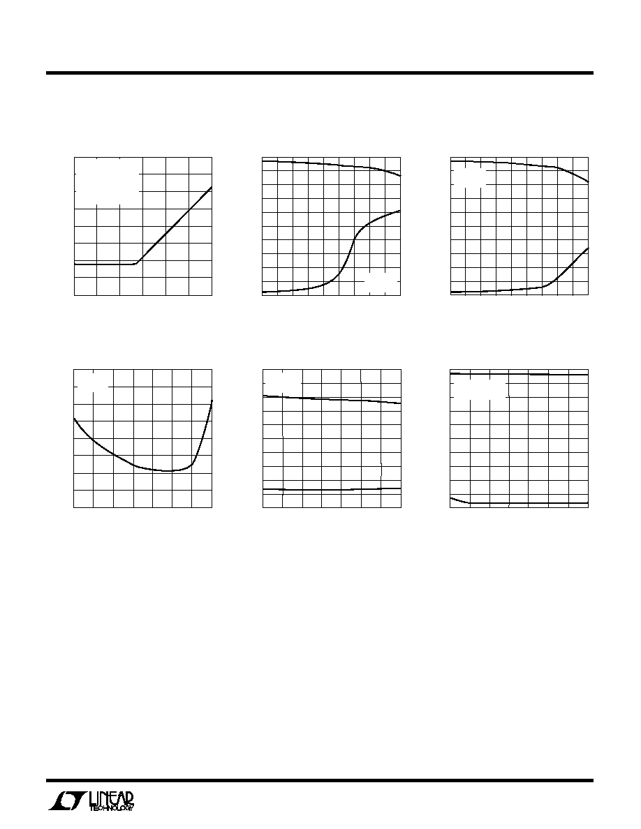
TYPICAL PERFOR
M
A
N
CE CHARACTERISTICS
U
W
LOAD RESISTANCE (
)
50
5
SINGLE-ENDED DRIVER OUTPUT (V)
4
2
1
0
5
2
200
500 1k
10k
LTC1323 · TPC03
3
3
4
1
100
300
2k
3k
5k
T
A
= 25°C
V
S
= 5V
Single-Ended Driver Swing
vs Load Resistance
LOAD RESISTANCE (
)
50
5
DIFFERENTIAL DRIVER OUTPUT (V)
4
2
1
0
5
2
200
500 1k
10k
LTC1323 · TPC02
3
3
4
1
100
300
2k
3k
5k
T
A
= 25°C
V
S
= 5V
Differential Driver Swing
vs Load Resistance
TEMPERATURE (°C)
50
0
DIFFERENTIAL DRIVER OUTPUT (V)
0.5
1.5
2.0
2.5
5.0
3.5
0
50
75
LTC1323 · TPC05
1.0
4.0
4.5
3.0
25
25
100
125
V
S
= 5V
R
L
= 100
TEMPERATURE (°C)
50
SUPPLY CURRENT (mA)
3.25
25
LTC1323 · TPC04
2.50
2.00
25
0
50
1.75
1.50
3.50
3.00
2.75
2.25
75
100
125
V
S
= 5V
NO LOAD
Differential Driver Swing
vs Temperature
Supply Current vs Temperature
LOAD CURRENT (mA)
0
CHARGE PUMP OUTPUT VOLTAGE (V)
4.5
4.0
3.5
15
25
LTC1323 · TPC01
5.0
5.5
6.0
5
10
20
3.0
2.5
2.0
30
T
A
= 25°C
V
S
= 5V
R
L(DIFF)
= 100
R
L(SE)
= 3k TO GND
V
TXI
= 5V
Charge Pump Output Voltage
vs Load Current
TEMPERATURE (°C)
50
5
SINGLE-ENDED DRIVER OUTPUT (V)
4
2
1
0
5
2
0
50
75
LTC1323 · TPC06
3
3
4
1
25
25
100
125
V
S
= 5V
R
L
= 3k TO GND
Single-Ended Driver Swing
vs Temperature