Äîêóìåíòàöèÿ è îïèñàíèÿ www.docs.chipfind.ru
1
LTC1263
12V, 60mA Flash Memory
Programming Supply
s
Guaranteed 60mA Output
s
Regulated 12V
±
5% Output Voltage
s
No Inductors
s
Supply Voltage Range: 4.75V to 5.5V
s
I
CC
0.5
µ
A Typ in Shutdown
s
Low Power: I
CC
= 300
µ
A
s
8-Pin SO Package
s
Same Pinout as LTC1262 and MAX662
The LTC
®
1263 is a regulated 12V, 60mA output DC/DC
converter. It provides the 12V
±
5% output necessary to
program double byte-wide flash memories. The output
provides 60mA from input voltages as low as 4.75V
without using any inductors. Only four external capacitors
are required to complete an extremely small, surface
mountable circuit. The output can be momentarily shorted
to ground without damaging the part.
The active high TTL compatible Shutdown pin can be
directly connected to a microprocessor. In the shutdown
mode, the supply current typically drops to 0.5
µ
A.
The LTC1263 is available in an 8-pin SO package.
FEATURES
DESCRIPTIO
N
U
, LTC and LT are registered trademarks of Linear Technology Corporation.
s
12V Flash Memory Programming Supplies
s
Compact 12V Op Amp Supplies
s
Battery-Powered Systems
APPLICATIO
N
S
U
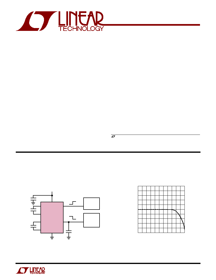
TYPICAL APPLICATIO
N
U
Flash Memory Programming Supply
Output Voltage vs Load
SHDN
V
OUT
C1
C1
+
C2
C2
+
LTC1263
0.47
µ
F
0.47
µ
F
LTC1263 · TA01
10
µ
F
V
CC
4.75V TO 5.5V
VPP
µ
P
FLASH
MEMORY
GND
V
CC
10
µ
F
ON
5V
SHDN
12V
LOAD CURRENT (mA)
0
20
40
60
80
100
OUTPUT VOLTAGE (V)
LTC1263 · TA02
13.0
12.8
12.6
12.4
12.2
12.0
11.8
11.6
11.4
11.2
11.0
2
LTC1263
ABSOLUTE
M
AXI
M
U
M
RATINGS
W
W
W
U
PACKAGE/ORDER I
N
FOR
M
ATIO
N
W
U
U
Consult factory for Industrial and Military grade parts and TSSOP package
option.
4.75V
V
CC
5.5V, T
A
= 0
°
C to 70
°
C (Notes 2, 3).
ELECTRICAL CHARACTERISTICS
SYMBOL
PARAMETER
CONDITIONS
MIN
TYP
MAX
UNITS
V
OUT
Output Voltage
0mA
I
OUT
60mA, V
SHDN
= 0V
q
11.4
12.6
V
I
CC
Supply Current
No Load, V
SHDN
= 0V
q
0.32
1.0
mA
I
SHDN
Shutdown Supply Current
No Load, V
SHDN
= V
CC
q
0.5
10
µ
A
f
OSC
Oscillator Frequency
V
CC
= 5V, I
OUT
= 60mA
300
kHz
Power Efficiency
V
CC
= 5V, I
OUT
= 60mA
76
%
R
SW
V
CC
to V
OUT
Switch Impedance
V
CC
= V
SHDN
= 5V, I
OUT
= 0mA
q
0.3
1
k
V
IH
SHDN Input High Voltage
q
2.4
V
V
IL
SHDN Input Low Voltage
q
0.8
V
SHDN Input Current
V
CC
= 5V, V
SHDN
= 0V
q
40
20
5
µ
A
V
CC
= 5V, V
SHDN
= 5V
q
10
0
10
µ
A
t
ON
Turn-On Time
C1 = C2 = 0.47
µ
F, C3 = C4 = 10
µ
F (Note 4) (Figures 1, 2)
600
µ
s
t
OFF
Turn-Off Time
C1 = C2 = 0.47
µ
F, C3 = C4 = 10
µ
F (Figures 1, 2)
10
ms
The
q
denotes specifications which apply over the full operating
temperature range.
Note 1: Absolute Maximum Ratings are those values beyond which the life
of a device may be impaired.
Note 2: All currents into device pins are positive; all currents out of device
pins are negative. All voltages are referenced to ground unless otherwise
specified.
Note 3: All typicals are given at V
CC
= 5V, T
A
= 25
°
C.
Note 4: A higher value output capacitor can be used but the "turn-on" and
"turn-off" time will increase proportionally.
(Note 1)
Supply Voltage (V
DD
) ................................................. 6V
Input Voltage (SHDN) ..................... 0.3V to V
CC
+ 0.3V
I
OUT
Continuous.................................................... 90mA
Operating Temperature Range ..................... 0
°
C to 70
°
C
Storage Temperature Range ................. 65
°
C to 150
°
C
Lead Temperature (Soldering, 10 sec).................. 300
°
C
T
JMAX
= 125
°
C,
JA
= 150
°
C/ W
1
2
3
4
8
7
6
5
TOP VIEW
SHDN
GND
V
OUT
V
CC
C1
C1
+
C2
C2
+
S8 PACKAGE
8-LEAD PLASTIC SO
LTC1263CS8
ORDER PART
NUMBER
3
LTC1263
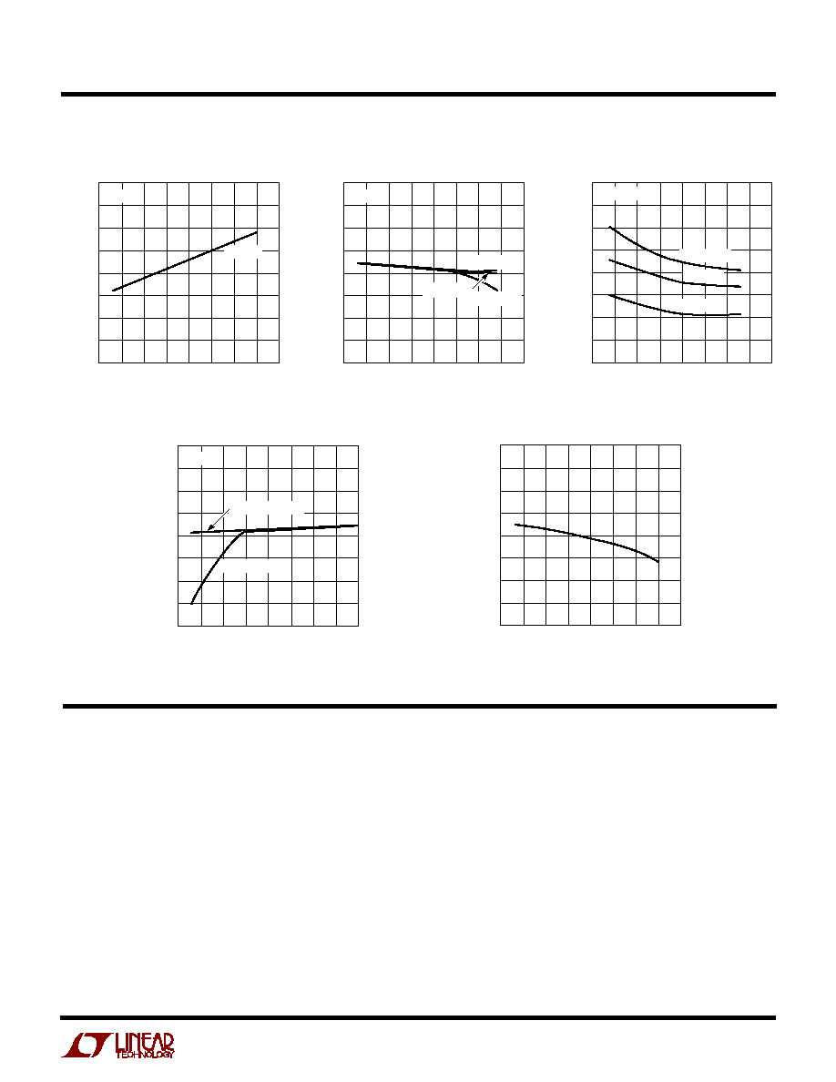
TYPICAL PERFOR
M
A
N
CE CHARACTERISTICS
U
W
Supply Current
Supply Current
TEMPERATURE (
°
C)
55
SUPPLY CURRENT (mA)
105
LTC1263 · TPC03
15
25
65
220
215
210
205
200
195
190
185
180
35
5
45
85
V
CC
= 4.75V
V
CC
= 5V
V
CC
= 5.5V
I
OUT
= 60mA
TEMPERATURE (
°
C)
55
SUPPLY CURRENT (
µ
A)
105
LTC1263 · TPC01
15
25
65
328
326
324
322
320
318
316
314
312
35
5
45
85
V
CC
= 5V
I
OUT
= 0
Output Voltage
Oscillator Frequency
SUPPLY VOLTAGE (V)
4.7
OUTPUT VOLTAGE (V)
5.5
LTC1263 · TPC04
4.9
5.1
5.3
12.8
12.6
12.4
12.2
12.0
11.8
11.6
11.4
11.2
4.8
5.0
5.2
5.4
I
OUT
= 90mA
I
OUT
= 0mA, 60mA
T
A
= 25
°
C
TEMPERATURE (
°
C)
55
FREQUENCY (kHz)
105
LTC1263 · TPC05
15
25
65
460
420
380
340
300
260
220
180
140
35
5
45
85
PI
N
FU
N
CTIO
N
S
U
U
U
C1
(Pin 1): First Charge Capacitor Negative Input. Connect
a 0.47
µ
F capacitor (C1) between C1
+
and C1
.
C1
+
(Pin 2): First Charge Capacitor Positive Input. Connect
a 0.47
µ
F capacitor (C1) between C1
+
and C1
.
C2
(Pin 3): Second Charge Capacitor Negative Input.
Connect a 0.47
µ
F capacitor (C2) between C2
+
and C2
.
C2
+
(Pin 4): Second Charge Capacitor Positive Input.
Connect a 0.47
µ
F capacitor (C2) between C2
+
and C2
.
V
CC
(Pin 5): Positive Supply Input. 4.75V
V
CC
5.5V.
Requires a 10
µ
F bypass capacitor to ground (C4).
V
OUT
(Pin 6): 12V Output. Requires a 10
µ
F or a higher
value bypass capacitor to ground (C3). V
OUT
= V
CC
when
in the shutdown mode.
GND (Pin 7): Ground.
SHDN (Pin 8): Active-High TTL Logic Level Shutdown Pin.
SHDN is internally pulled up to V
CC
. Connect to GND for
normal operation. In shutdown mode, the charge pump is
turned off and V
OUT
= V
CC
.
Output Voltage
TEMPERATURE (
°
C)
55
OUTPUT VOLTAGE (V)
105
LTC1263 · TPC02
15
25
65
12.8
12.6
12.4
12.2
12.0
11.8
11.6
11.4
11.2
35
5
45
85
I
OUT
= 0mA
I
OUT
= 90mA
I
OUT
= 60mA
V
CC
= 5V
4
LTC1263
BLOCK DIAGRA
M
W
+
C1
+
C1
C1
C2
+
C2
C2
S4B
S4A
S3A
S3C
S1
R1
R2
R3
BANDGAP
REFERENCE
OSCILLATOR
V
CC
V
OUT
C
IN
C
OUT
SHDN
GND
CHARGE PUMP
S4C
S3D
S3B
LTC1263 · BD
V
BGAP
S1 AND S2 SHOWN WITH SHDN PIN LOW. S3A, S3B, S3C, S3D, S4A, S4B AND S4C SHOWN CHARGING C1 AND C2
WITH OSCILLATOR OUTPUT LOW AND V
DIV
< V
BGAP
V
HYST
. AT OSCILLATOR OUTPUT HIGH, S3A, S3B, S3C AND S3D
OPEN WHILE S4A, S4B AND S4C CLOSE TO CHARGE V
OUT
. COMPARATOR HYSTERESIS IS
±
V
HYST
S2
V
DIV
CLK
TI
M
I
N
G DIAGRA
M
S
W
U
W
1.4V
1.4V
V
SHDN
V
OUT
5.1V
12V
t
ON
t
OFF
V
OUT
V
CC
V
CC
0V
LTC1263 · F01
Figure 1. Timing Diagram
1
2
3
4
8
7
6
5
SHDN
GND
V
OUT
V
CC
C1
C1
+
C2
C2
+
LTC1263
C1 = 0.47
µ
F
C2 = 0.47
µ
F
LTC1263 · F02
C3 = 10
µ
F
C4 = 10
µ
F
V
CC
4.75V TO 5.5V
V
SHDN
V
OUT
Figure 2. Timing Circuit
5
LTC1263
The LTC1263 uses a charge pump tripler to generate 12V
from a V
CC
of 5V. The charge pump is clocked by an
internal oscillator. The oscillator frequency is not critical
and may vary from the typical value of 300kHz. When the
oscillator output is low, C1 and C2 are each connected
between V
CC
and GND, charging them to V
CC
(see Figure
3). When the oscillator output goes high, C1 and C2 are
stacked in series with the bottom plate of C1 pulled to V
CC
(see Figure 4). The top plate of C2 is switched to charge
C
OUT
, which enables V
OUT
to rise.
V
OUT
is regulated to within 5% of 12V by an oscillator pulse
gating scheme that turns the charge pump on and off
based on the comparator results of V
OUT
and a reference
voltage. First, a resistor divider senses V
OUT
; if the output
of the divider (V
DIV
) is less than the output of a bandgap
(V
BGAP
) by the hysteresis voltage (V
HYST
) of the compara-
tor, then oscillator pulses are applied to the charge pump
to raise V
OUT
. When V
DIV
is above V
BGAP
by V
HYST
, the
OPERATIO
N
U
oscillator pulses are prevented from clocking the charge
pump. As a result, V
OUT
drops until V
DIV
is below V
BGAP
by
V
HYST
again.
To ensure proper start-up when V
OUT
is lower than V
CC
and maintain proper operation when V
OUT
is higher than
V
CC
, the gates of all internal switches are driven between
GND and the higher of either V
OUT
or V
CC
.
To reduce supply current, the LTC1263 may be put into
shutdown mode by "floating" the SHDN pin or connecting
it to V
CC
. In this mode, the bandgap, comparator, oscilla-
tor and resistor divider are switched off to reduce the
supply current to typically 0.5
µ
A. At the same time an
internal switch shorts V
OUT
to V
CC
; V
OUT
takes 10ms (typ)
to reach 5.1V (see t
OFF
in Figure 1). When the SHDN pin
is low, the LTC1263 exits shutdown and the charge pump
operates to raise V
OUT
to 12V. V
OUT
takes 600
µ
s (typ) to
reach the lower regulation limit of 11.4V (see t
ON
in Figure 1).
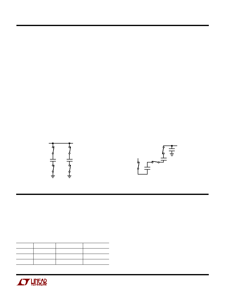
+
C1
+
C2
V
CC
LTC1263 · F03
Figure 3. C1 and C2 Charge to V
CC
Figure 4. C1 and C2 Stacked in Series with C1
Tied to V
CC
+
C1
+
C2
V
CC
LTC1263 · F04
V
OUT
C
OUT
APPLICATIO
N
S I
N
FOR
M
ATIO
N
W
U
U
U
Choice of Capacitors
The LTC1263 is tested with the capacitors shown in Figure
2. C1 and C2 are 0.47
µ
F ceramic capacitors and C
IN
and
C
OUT
are 10
µ
F tantalum capacitors. Refer to Table 1 if
other choices are desired.
Table 1. Recommended Capacitor Types and Values
CAPACITOR
CERAMIC
TANTALUM
ALUMINUM
C1, C2
0.47
µ
F to 1
µ
F
Not Recommended Not Recommended
C
OUT
10
µ
F (Min)
10
µ
F (Min)
10
µ
F (Min)
C
IN
10
µ
F (Min)
10
µ
F (Min)
10
µ
F (Min)
C1 and C2 should be ceramic capacitors with values in the
range of 0.47
µ
F to 1
µ
F. Higher values provide better load
regulation. Tantalum capacitors are not recommended as
the higher ESR of these capacitors degrades performance
at high load currents and V
CC
= 4.75V.
C
IN
and C
OUT
can be ceramic, tantalum or electrolytic
capacitors. The ESR of C
OUT
introduces steps in the V
OUT
waveform whenever the charge pump charges C
OUT
. This
tends to increase V
OUT
ripple. Ceramic or tantalum capaci-
tors are recommended for C
OUT
if minimum ripple is