Äîêóìåíòàöèÿ è îïèñàíèÿ www.docs.chipfind.ru
1
LTC1261
S
FEATURE
D
U
ESCRIPTIO
s
Regulated Negative Voltage from a
Single Positive Supply
s
Can Provide Regulated 5V from a 3V Supply
s
REG Pin Indicates Output is in Regulation
s
Low Output Ripple: 5mV Typ
s
Supply Current: 600
µ
A Typ
s
Shutdown Mode Drops Supply Current to 5
µ
A
s
Up to 15mA Output Current
s
Adjustable or Fixed Output Voltages
s
Requires Only Three or Four External Capacitors
s
Available in SO-8 Packages
The LTC
®
1261 is a switched-capacitor voltage inverter
designed to provide a regulated negative voltage from a
single positive supply. The LTC1261CS operates from a
single 3V to 8V supply and provides an adjustable output
voltage from 1.25V to 8V. An on-chip resistor string
allows the LTC1261CS to be configured for output volt-
ages of 3.5V, 4V, 4.5V or 5V with no external
components. The LTC1261CS8 is optimized for applica-
tions which use a 5V or higher supply or which require
low output voltages. It requires a single external 0.1
µ
F
capacitor and provides adjustable and fixed output voltage
options in 8-pin SO packages. The LTC1261CS requires
one or two external 0.1
µ
F capacitors, depending on input
voltage. Both versions require additional external input
and output bypass capacitors. An optional compensation
capacitor at ADJ/COMP can be used to reduce the output
voltage ripple.
Each version of the LTC1261 will supply up to 12mA
output current with guaranteed output regulation of 5%.
The LTC1261 includes an open-drain REG output which
pulls low when the output is within 5% of the set value.
Output ripple is typically as low as 5mV. Quiescent current
is typically 600
µ
A when operating and 5
µ
A in shutdown.
The LTC1261 is available in a 14-pin narrow body SO
package and an 8-pin SO package.
Switched Capacitor
Regulated Voltage Inverter
s
GaAs FET Bias Generators
s
Negative Supply Generators
s
Battery-Powered Systems
s
Single Supply Applications
U
S
A
O
PPLICATI
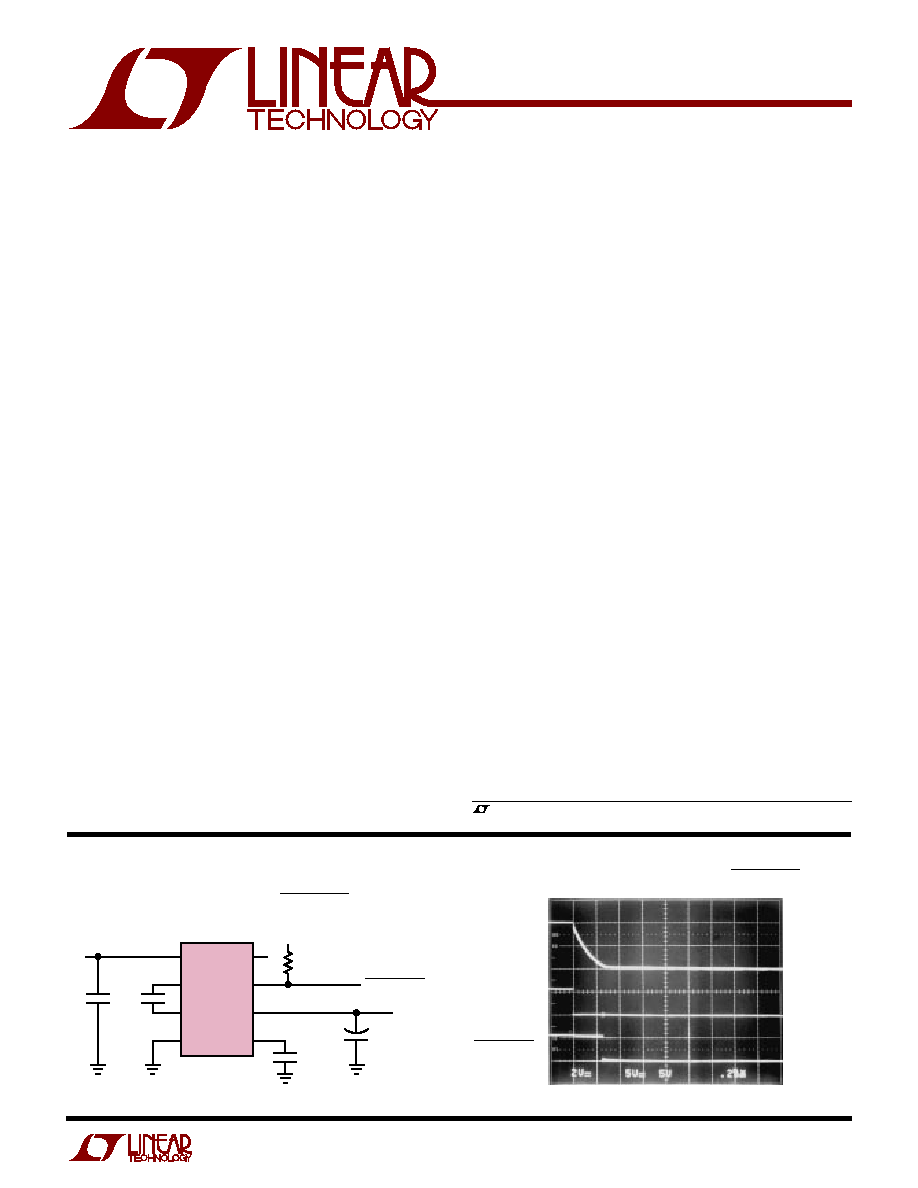
TYPICAL APPLICATIO
N
U
4V Generator with Power Valid
, LTC and LT are registered trademarks of Linear Technology Corporation.
1
2
3
4
8
7
6
5
LTC1261-4
SHDN
REG
OUT
COMP
V
CC
C1
+
C1
GND
C2
0.1
µ
F
LTC1261 · TA01
C4
3.3
µ
F
V
OUT
= 4V
AT 10mA
POWER VALID
5V
C1
1
µ
F
5V
10k
C3*
100pF
*OPTIONAL
+
Waveforms for 4V Generator with Power Valid
0V
OUT
4V
5V
SHDN
0V
5V
POWER VALID
0V
0.2mS/DIV
LTC1261 · TAO2
2
LTC1261
A
U
G
W
A
W
U
W
A
R
BSOLUTE
XI
TI
S
W
U
U
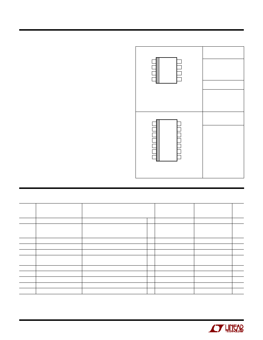
PACKAGE/ORDER I FOR ATIO
LTC1261CS8
LTC1261CS8-4
LTC1261CS8-4.5
S8 PART MARKING
1261
12614
126145
Consult factory for Industrial or Military grade parts.
LTC1261CS
ELECTRICAL C
C
HARA TERISTICS
0
°
C
T
A
70
°
C
40
°
C
T
A
85
°
C
(Note 7)
SYMBOL
PARAMETER
CONDITIONS
MIN
TYP
MAX
MIN
TYP
MAX
UNITS
V
REF
Reference Voltage
q
1.20
1.24
1.28
1.20
1.24
1.28
V
I
S
Supply Current
No Load, SHDN Floating, Doubler Mode
q
600
1000
600
1500
µ
A
No Load, SHDN Floating, Tripler Mode
q
900
1500
900
2000
µ
A
No Load, V
SHDN
= V
CC
q
5
20
5
20
µ
A
f
OSC
Internal Oscillator Frequency
550
550
kHz
P
EFF
Power Efficiency
65
65
%
V
OL
REG Output Low Voltage
I
REG
= 1mA
q
0.1
0.8
0.1
0.8
V
I
REG
REG Sink Current
V
REG
= 0.8V, V
CC
= 3.3V
q
5
8
5
8
mA
V
REG
= 0.8V, V
CC
= 5.0V
q
8
15
8
15
mA
I
ADJ
Adjust Pin Current
V
ADJ
= 1.24V
q
0.01
1
0.01
1
µ
A
V
IH
SHDN Input High Voltage
q
2
2
V
V
IL
SHDN Input Low Voltage
q
0.8
0.8
V
I
IN
SHDN Input Current
V
SHDN
= V
CC
q
5
20
5
25
µ
A
t
ON
Turn-On Time
I
OUT
= 15mA
500
500
µ
s
ORDER PART
NUMBER
ORDER PART
NUMBER
T
JMAX
= 150
°
C,
JA
= 150
°
C/W
T
JMAX
= 150
°
C,
JA
= 110
°
C/W
V
CC
= 3V to 6.5V, T
A
= 25
°
C unless otherwise specified.
1
2
3
4
8
7
6
5
TOP VIEW
SHDN
REG
OUT
ADJ (COMP*)
V
CC
C1
+
C1
GND
S8 PACKAGE
8-LEAD PLASTIC SO
*FOR FIXED VERSIONS
TOP VIEW
S PACKAGE
14-LEAD PLASTIC SO
1
2
3
4
5
6
7
14
13
12
11
10
9
8
NC
C1
+
C1
C2
+
C2
GND
R0
V
CC
SHDN
REG
OUT
ADJ
R
ADJ
R1
(Note 1)
Supply Voltage (Note 2)............................................ 9V
Output Voltage (Note 5) .............................. 0.3V to 9V
Total Voltage, V
CC
to V
OUT
(Note 2) ........................ 12V
Input Voltage
SHDN Pin ................................. 0.3V to V
CC
+ 0.3V
REG Pin ............................................... 0.3V to 12V
ADJ, R
O,
R1, R
ADJ ...............
V
OUT
0.3V to V
CC
+ 0.3V
Output Short-Circuit Duration ......................... Indefinite
Operating Temperature Range
Commercial ............................................ 0
°
C to 70
°
C
Extended Commercial (Note 7) .......... 40
°
C to 85
°
C
Storage Temperature Range ................ 65
°
C to 150
°
C
Lead Temperature (Soldering, 10 sec)................. 300
°
C
3
LTC1261
ELECTRICAL C
C
HARA TERISTICS
0
°
C
T
A
70
°
C
40
°
C
T
A
85
°
C
(Note 7)
SYMBOL PARAMETER
CONDITIONS (Note 2)
MIN
TYP
MAX
MIN
TYP
MAX
UNITS
V
OUT
Output Regulation
1.24V
V
OUT
4V, 0
I
OUT
8mA
q
1
5
%
(Note 2)
1.24V
V
OUT
4V, 0
I
OUT
7mA
q
1
5
%
4V
V
OUT
5V, 0
I
OUT
8mA (Note 6)
2
2
%
I
SC
Output Short-Circuit Current
V
OUT
= 0V
q
60
125
60
125
mA
V
RIP
Output Ripple Voltage
I
OUT
= 5mA, V
OUT
= 4V
5
5
mV
Doubler Mode. V
CC
= 5V
±
10%, C1 = 0.1
µ
F, C2 = 0 (Note 4), C
OUT
= 3.3
µ
F unless otherwise specified.
LTC1261CS Only. Tripler Mode. V
CC
= 2.7V, C1 = C2 = 0.1
µ
F (Note 4), C
OUT
= 3.3
µ
F unless otherwise specified.
0
°
C
T
A
70
°
C
40
°
C
T
A
85
°
C
(Note 7)
SYMBOL PARAMETER
CONDITIONS (Note 2)
MIN
TYP
MAX
MIN
TYP
MAX
UNITS
V
OUT
Output Regulation
1.24V
V
OUT
4V, 0
I
OUT
5mA
q
1
5
1
5
%
I
SC
Output Short-Circuit Current
V
OUT
= 0V
q
60
125
60
125
mA
V
RIP
Output Ripple Voltage
I
OUT
= 5mA, V
OUT
= 4V
5
5
mV
0
°
C
T
A
70
°
C
40
°
C
T
A
85
°
C
(Note 7)
SYMBOL PARAMETER
CONDITIONS (Note 2)
MIN
TYP
MAX
MIN
TYP
MAX
UNITS
V
OUT
Output Regulation
1.24V
V
OUT
4.5V, 0
I
OUT
6mA
q
1
5
1
5
%
(Note 2)
4.5V
V
OUT
5V, 0
I
OUT
3.5mA
q
2
5
2
%
I
SC
Output Short-Circuit Current
V
OUT
= 0V
q
35
75
35
75
mA
V
RIP
Output Ripple Voltage
I
OUT
= 5mA, V
OUT
= 4V
5
5
mV
0
°
C
T
A
70
°
C
40
°
C
T
A
85
°
C
(Note 7)
SYMBOL PARAMETER
CONDITIONS (Note 2)
MIN
TYP
MAX
MIN
TYP
MAX
UNITS
V
OUT
Output Regulation
1.24V
V
OUT
4V, 0
I
OUT
12mA
q
1
5
1
5
%
4V
V
OUT
5V, 0
I
OUT
10mA
q
2
5
2
5
%
I
SC
Output Short-Circuit Current
V
OUT
= 0V
q
35
75
35
75
mA
V
RIP
Output Ripple Voltage
I
OUT
= 5mA, V
OUT
= 4V
5
5
mV
LTC1261CS Only. Tripler Mode. V
CC
= 5V
±
10%, C1 = C2 = 0.1
µ
F (Note 4), C
OUT
= 3.3
µ
F unless otherwise specified.
LTC1261CS Only. Tripler Mode. V
CC
= 3.3V
±
10%, C1 = C2 = 0.1
µ
F (Note 4), C
OUT
= 3.3
µ
F unless otherwise specified.
to C2
with C1
and C2
+
floating. For the LTC1261CS8 in doubler mode,
C1 connects from C1
+
to C1
; there are no C2 pins.
Note 5: Setting output to < 7V will exceed the absolute voltage maximum
rating with a 5V supply. With supplies higher than 5V, the output should
never be set to exceed V
CC
12V.
Note 6: For output voltages below 4.5V the LTC1261 may reach 50%
duty cycle and fall out of regulation with heavy load or low input voltages.
Beyond this point, the output will follow the input with no regulation.
Note 7: C grade device specifications are guaranteed over the 0
°
C to 70
°
C
temperature range. In addition, C grade device specifications are assured
over the 40
°
C to 85
°
C temperature range by design or correlation, but
are not production tested.
The
q
denotes specifications which apply over the full operating
temperature range.
Note 1: The Absolute Maximum Ratings are those values beyond which
the life of a device may be impaired.
Note 2: All currents into device pins are positive; all currents out of device
pins are negative. All voltages are referenced to ground unless otherwise
specified.
Note 3: All typicals are given at T
A
= 25
°
C.
Note 4: C1 = C2 = 0.1
µ
F means the specifications apply to tripler mode
where V
CC
V
OUT
= 3V
CC
(LTC1261CS only; the LTC1261CS8 cannot be
connected in tripler mode) with C1 connected between C1
+
and C1
and
C2 connected between C2
+
and C2
. C2 = 0 implies doubler mode where
V
CC
V
OUT
= 2V
CC
; for the LTC1261CS this means C1 connects from C1
+
4
LTC1261
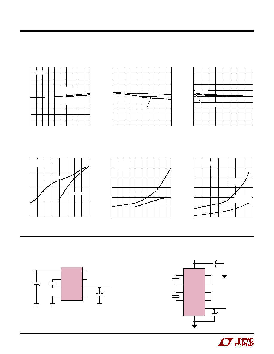
TYPICAL PERFOR
M
A
N
CE CHARACTERISTICS
U
W
Maximum Output Current
vs Supply Voltage
Supply Current
vs Supply Voltage
Output Voltage
vs Output Current
Output Voltage (Doubler Mode)
vs Supply Voltage
Output Voltage (Tripler Mode)
vs Supply Voltage
OUTPUT CURRENT (mA)
0
OUTPUT VOLTAGE (V)
3.9
3.7
3.5
3.6
3.8
4.0
4.2
4.4
8
LT1261 · TP01
4.1
4.3
4.5
2
1
3
5
7
9
4
6
10
V
CC
= 5V
DOUBLER MODE
V
CC
= 3.3V
TRIPLER MODE
T
A
= 25
°
C
SUPPLY VOLTAGE (V)
5.0
OUTPUT VOLTAGE (V)
3.9
3.7
3.5
3.6
3.8
4.0
4.2
4.4
6.6
LT1261 · TP02
4.1
4.3
4.5
5.4
5.2
5.6
6.0
6.4
6.8
5.8
6.2
7.0
T
A
= 85
°
C
T
A
= 25
°
C
T
A
= 40
°
C
SUPPLY VOLTAGE (V)
3
4.5
4.4
4.3
4.2
4.1
4.0
3.9
3.8
3.7
3.6
3.5
OUTPUT VOLTAGE (V)
4
5
LTC1261 · TPC03
6
7
T
A
= 85
°
C
T
A
= 25
°
C
T
A
= 40
°
C
Supply Current
vs Temperature
SUPPLY VOLTAGE (V)
3.0
10
MAXIMUM OUTPUT CURRENT (mA)
20
30
40
50
3.5
4.0
4.5
5.0
LTC1261 · TPC04
5.5
6.0
6.5
7.0
V
OUT
= 4V
±
5%
T
A
= 25
°
C
TRIPLER MODE
DOUBLER MODE
SUPPLY VOLTAGE (V)
500
1000
600
800
SUPPLY CURRENT (
µ
A)
700
900
1200
3.5
4.5
5.5
6.5
LTC1261 · TPC05
7.5 8.0
3.0
4.0
5.0
6.0
7.0
V
OUT
= 4V
T
A
= 25
°
C
TRIPLER MODE
DOUBLER MODE
TEMPERATURE (°C)
40
SUPPLY CURRENT (
µ
A)
900
1000
1200
20
60
LTC1261 · TPC06
800
700
20
0
40
80
100
600
500
V
OUT
= 4V
V
CC
= 5V
DOUBLER MODE
V
CC
= 3.3V
TRIPLER MODE
(See Test Circuits)
Doubler Mode
1
2
3
4
8
7
6
5
LTC1261-4
SHDN
REG
OUT
COMP
V
CC
C1
+
C1
GND
0.1
µ
F
LTC1261 · TCO1
3.3
µ
F
V
OUT
= 4V
±
5%
5V
10
µ
F
+
+
2
3
4
5
10
9
8
7
11
ADJ
R
ADJ
R1
R0
OUT
C1
+
C1
C2
+
C2
0.1
µ
F
LTC1261 · TC02
6
14
0.1
µ
F
10
µ
F
LTC1261CS
V
IN
= 3.3V
V
CC
GND
3.3
µ
F
V
OUT
= 4V
±
5%
+
+
TEST CIRCUITS
Tripler Mode

5
LTC1261
PI
N
FU
N
CTIO
N
S
U
U
U
Pin numbers are shown as (LTC1261CS/LTC1261CS8).
NC (Pin 1/NA): No Internal Connection.
C1
+
(Pin 2/ Pin 2): C1 Positive Input. Connect a 0.1
µ
F
capacitor between C1
+
and C1
. With the LTC1261CS in
doubler mode, connect a 0.1
µ
F capacitor from C1
+
to
C2
.
C1
(Pin 3/Pin 3): C1 Negative Input. Connect a 0.1
µ
F
capacitor from C1
+
to C1
. With the LTC1261CS in
doubler mode only, C1
should float.
C2
+
(Pin 4/NA): C2 Positive Input. In tripler mode con-
nect a 0.1
µ
F capacitor from C2
+
to C2
. This pin is used
with the LTC1261CS in tripler mode only; in doubler
mode this pin should float.
C2
(Pin 5/NA): C2 Negative Input. In tripler mode
connect a 0.1
µ
F capacitor from C2
+
to C2
. In doubler
mode connect a 0.1
µ
F capacitor from C1
+
to C2
.
GND (Pin 6/Pin 4): Ground. Connect to a low impedance
ground. A ground plane will help to minimize regulation
errors.
R0 (Pin 7/NA): Internal Resistor String, 1st Tap. See
Table 2 in the Applications Information section for infor-
mation on internal resistor string pin connections vs
output voltage.
R1 (Pin 8/NA): Internal Resistor String, 2nd Tap.
R
ADJ
(Pin 9/NA): Internal Resistor String Output. Con-
nect this pin to ADJ to use the internal resistor divider.
See Table 2 in the Applications Information section for
information on internal resistor string pin connections vs
output voltage.
ADJ (COMP for fixed versions) (Pin 10/Pin 5): Output
Adjust/Compensation Pin. For adjustable parts this pin is
used to set the output voltage. The output voltage should
be divided down with a resistor divider and fed back to
this pin to set the regulated output voltage. The resistor
divider can be external or the internal divider string can
be used if it can provide the required output voltage.
Typically the resistor string should draw
10
µ
A from the
output to minimize errors due to the bias current at the
adjust pin. Fixed output parts have the internal resistor
string connected to this pin inside the package. The pin
can be used to trim the output voltage if desired. It can
also be used as an optional feedback compensation pin
to reduce output ripple on both adjustable and fixed
output voltage parts. See Applications Information sec-
tion for more information on compensation and output
ripple.
OUT (Pin 11/Pin 6): Negative Voltage Output. This pin
must be bypassed to ground with a 1
µ
F or larger capaci-
tor; it must be at least 3.3
µ
F to provide specified output
ripple. The size of the output capacitor has a strong effect
on output ripple. See the Applications Information sec-
tion for more details.
REG (Pin 12/Pin 7): This is an open drain output that pulls
low when the output voltage is within 5% of the set value.
It will sink 8mA to ground with a 5V supply. The external
circuitry must provide a pull-up or REG will not swing
high. The voltage at REG may exceed V
CC
and can be
pulled up to 12V above ground without damage.
SHDN (Pin 13/Pin 8): Shutdown. When this pin is at
ground the LTC1261 operates normally. An internal 5
µ
A
pull-down keeps SHDN low if it is left floating. When
SHDN is pulled high, the LTC1261 enters shutdown
mode. In shutdown the charge pump stops, the output
collapses to 0V and the quiescent current drops to 5
µ
A
typically.
V
CC
(Pin 14/Pin 1): Power Supply. This requires an input
voltage between 3V and 6.5V. Certain combinations of
output voltage and operating mode may place additional
restrictions on the input voltage. V
CC
must be bypassed
to ground with at least a 0.1
µ
F capacitor placed in close
proximity to the chip. See the Applications Information
section for details.