Äîêóìåíòàöèÿ è îïèñàíèÿ www.docs.chipfind.ru
1
LTC1144
Switched-Capacitor
Wide Input Range
Voltage Converter
with Shutdown
U
A
O
PPLICATI
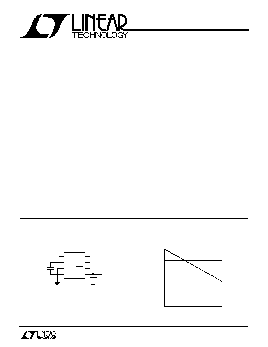
TYPICAL
Output Voltage vs Load Current, V
+
= 15V
S
FEATURE
D
U
ESCRIPTIO
s
Wide Operating Supply Voltage Range: 2V to 18V
s
Boost Pin (Pin 1) for Higher Switching Frequency
s
Simple Conversion of 15V to 15V Supply
s
Low Output Resistance: 120
Maximum
s
Power Shutdown to 8
µ
A with SHDN Pin
s
Open Circuit Voltage Conversion Efficiency:
99.9% Typical
s
Power Conversion Efficiency: 93% Typical
s
Easy to Use
The LTC1144 is a monolithic CMOS switched-capacitor
voltage converter. It performs supply voltage conversion
from positive to negative from an input range of 2V to 18V,
resulting in complementary output voltages of 2V to
18V. Only two noncritical external capacitors are needed
for the charge pump and charge reservoir functions.
The converter has an internal oscillator that can be
overdriven by an external clock or slowed down when
connected to a capacitor. The oscillator runs at a 10kHz
frequency when unloaded. A higher frequency outside the
audio band can also be obtained if the Boost Pin is tied to
V
+
. The SHDN pin reduces supply current to 8
µ
A and can
be used to save power when the converter is not in use.
The LTC1144 contains an internal oscillator, divide-by-
two, voltage level shifter, and four power MOSFETs. A
special logic circuit will prevent the power N-channel
switch substrate from turning on.
U
S
A
O
PPLICATI
s
Conversion of 15V to
±
15V Supplies
s
Inexpensive Negative Supplies
s
Data Acquisition Systems
s
High Voltage Upgrade to LTC1044 or 7660
s
Voltage Division and Multiplications
s
Automotive Applications
s
Battery Systems with Wall Adapter/Charger
LOAD CURRENT (mA)
0
10
OUTPUT VOLTAGE (V)
15
14
13
12
11
10
40
1144 TA02
20
30
50
R
OUT
= 56
T
A
= 25°C
1
2
3
4
8
7
6
5
BOOST
CAP
+
GND
CAP
V
+
OSC
SHDN
V
OUT
+
+
10
µ
F
15V OUTPUT
15V INPUT
LTC1144
10
µ
F
1144 TA01
Generating 15V from 15V
2
LTC1144
W
U
U
PACKAGE/ORDER I FOR ATIO
A
U
G
W
A
W
U
W
A
R
BSOLUTE
XI
TI
S
(Note 1)
Supply Voltage (V
+
) (Transient) .............................. 20V
Supply Voltage (V
+
) (Operating) ............................. 18V
Input Voltage on Pins 1, 6, 7
(Note 2) ............................ 0.3V < V
IN
< (V
+
) + 0.3V
Output Short-Circuit Duration
V
+
10V .................................................... Indefinite
V
+
15V ........................................................ 30 sec
V
+
20V ............................................. Not Protected
Power Dissipation ............................................. 500mW
Operating Temperature Range
LTC1144C ................................................ 0
°
C to 70
°
C
LTC1144I ............................................ 40
°
C to 85
°
C
Storage Temperature Range ................. 65
°
C to 150
°
C
Lead Temperature (Soldering, 10 sec) .................. 300
°
C
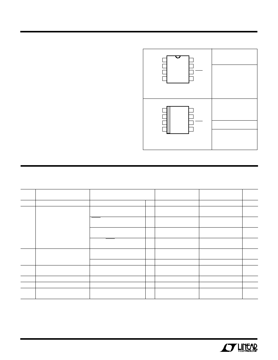
TOP VIEW
1
2
3
4
8
7
6
5
BOOST
CAP
+
GND
CAP
V
+
OSC
SHDN
V
OUT
S8 PACKAGE
8-LEAD PLASTIC SOIC
T
JMAX
= 110°C,
JA
= 130°C/W
1
2
3
4
8
7
6
5
TOP VIEW
BOOST
CAP
+
GND
CAP
V
+
OSC
SHDN
V
OUT
N8 PACKAGE
8-LEAD PLASTIC DIP
T
JMAX
= 110°C,
JA
= 100°C/W
S8 PART MARKING
1144
1144I
LTC1144CS8
LTC1144IS8
LTC1144CN8
LTC1144IN8
ORDER PART
NUMBER
Consult factory for Military grade parts.
The
q
denotes specifications which apply over the full operating
temperature range; all other limits and typicals at T
A
= 25
°
C.
Note 1: Absolute maximum ratings are those values beyond which the life
of a device may be impaired.
Note 2: Connecting any input terminal to voltages greater than V
+
or less
than ground may cause destructive latch-up. It is recommended that no
inputs from sources operating from external supplies be applied prior to
power-up of the LTC1144.
Note 3: f
OSC
is tested with C
OSC
= 100pF to minimize the effects of test
fixture capacitance loading. The 0pF frequency is correlated to this 100pF
test point, and is intended to simulate the capacitance at pin 7 when the
device is plugged into a test socket and no external capacitor is used.
LTC1144C
LTC1144I
SYMBOL PARAMETER
CONDITIONS
MIN
TYP
MAX
MIN
TYP
MAX
UNITS
Supply Voltage Range
R
L
= 10k
q
2
18
2
18
V
I
S
Supply Current
R
L
=
, Pins 1, 6 No Connection,
1.1
1.1
mA
f
OSC
= 10kHz
q
1.3
1.6
mA
SHDN = 0V, R
L
=
, Pins 1, 7
q
0.008
0.03
0.008
0.035
mA
No Connection
V
+
= 5V, R
L
=
, Pins 1, 6
0.10
0.10
mA
No Connection, f
OSC
= 4kHz
q
0.13
0.15
mA
V
+
= 5V, SHDN = 0V, R
L
=
,
q
0.002
0.015
0.002
0.018
mA
Pins 1, 7 No Connection
R
OUT
Output Resistance
V
+
= 15V, I
L
= 20mA at 10kHz
56
100
56
100
q
120
140
V
+
= 5V, I
L
= 3mA at 4kHz
q
90
250
90
300
f
OSC
Oscillator Frequency
V
+
= 15V (Note 3)
10
10
kHz
V
+
= 5V
4
4
kHz
Power Efficiency
R
L
= 2k at 10kHz
q
90
93
90
93
%
Voltage Conversion Efficiency
R
L
=
q
97.0
99.9
97.0
99.9
%
Oscillator Sink or Source Current
V
+
= 5V (V
OSC
= 0V to 5V)
0.5
0.5
µ
A
V
+
= 15V (V
OSC
= 0V to 15V)
4
4
µ
A
ELECTRICAL C
C
HARA TERISTICS
V
+
= 15V, C
OSC
= 0pF, T
A
= 25
°
C, Test Circuit Figure 1, unless otherwise noted.
3
LTC1144
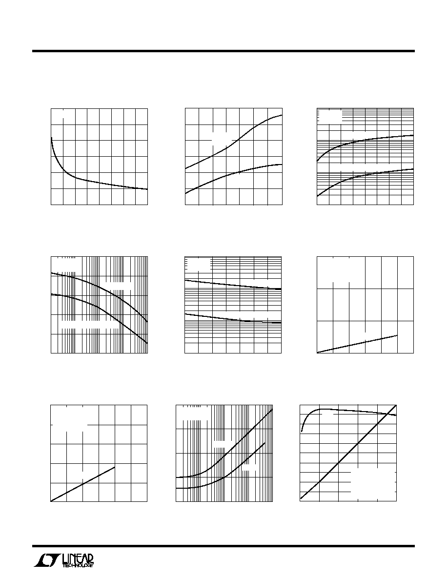
TYPICAL PERFOR
M
A
N
CE CHARACTERISTICS
U
W
SUPPLY VOLTAGE (V)
2
OSCILLATOR FREQUENCY (kHz)
10
100
1000
6
10
14
4
8
12
16
18
LTC1144 · TPC03
1
T
A
= 25°C
C
OSC
= 0
BOOST = V
+
BOOST = OPEN OR GROUND
Oscillator Frequency
vs Supply Voltage
Output Resistance
vs Supply Voltage
SUPPLY VOLTAGE (V)
2
0
OUTPUT RESISTANCE (
)
50
100
150
200
6
10
14
18
LTC1144 · TPC01
250
300
4
8
12
16
T
A
= 25°C
TEMPERATURE (°C)
55
OUTPUT RESISTANCE (
)
100
120
140
25
75
LTC1144 · TPC02
80
60
25
0
50
100
125
40
20
V
+
= 5V
I
L
= 3mA
V
+
= 15V
I
L
= 20mA
Output Resistance vs Temperature
Oscillator Frequency
vs Temperature
Output Voltage vs Load Current
Oscillator Frequency as a
Function of C
OSC
EXTERNAL CAPACITANCE (PIN 7 TO GND), C
OSC
(pF)
1
OSCILLATOR FREQUENCY (kHz)
1
10
10000
LTC1144 · TPC04
0.1
0.01
10
100
1000
1000
100
T
A
= 25°C
V
+
= 15V
BOOST = OPEN OR GROUND
BOOST = V
+
LOAD CURRENT (mA)
0
15
OUTPUT VOLTAGE (V)
10
5
0
10
20
30
40
LTC1144 · TPC06
50
60
T
A
= 25°C
V
+
= 15V
C1 = C2 = 10
µ
F
BOOST = OPEN
R
OUT
= 56
TEMPERATURE (°C)
55
25
OSCILLATOR FREQUENCY (kHz)
10
100
1000
0
25
50
75
100
125
LTC1144 · TPC05
1
BOOST = V
+
BOOST = OPEN OR GROUND
T
A
= 25°C
V
+
= 15V
Power Conversion Efficiency and
Supply Current vs Load Current
LOAD CURRENT (mA)
0
5
OUTPUT VOLTAGE (V)
4
3
2
1
0
5
10
15
20
LTC1144 · TPC07
25
30
T
A
= 25°C
V
+
= 5V
C1 = C2 = 10
µ
F
BOOST = OPEN
R
OUT
= 90
Output Voltage vs Load Current
Supply Current as a Function of
Oscillator Frequency
OSCILLATOR FREQUENCY (kHz)
0.01
SUPPLY CURRENT (
µ
A)
100
1000
100
LTC1144 · TPC08
10
1
0.1
1
10
10000
T
A
= 25°C
C1 = C2 = 10
µ
F
V
+
= 15V
V
+
= 5V
LOAD CURRENT (mA)
0
POWER CONVERSION EFFICIENCY (%)
SUPPLY CURRENT (mA)
60
80
100
40
LTC1144 · TPC09
40
20
0
60
80
100
40
20
0
10
20
30
50
P
EFF
I
S
T
A
= 25°C
V
+
= 15V
C1 = C2 = 10
µ
F
BOOST = OPEN
(SEE TEST CIRCUIT)
4
LTC1144
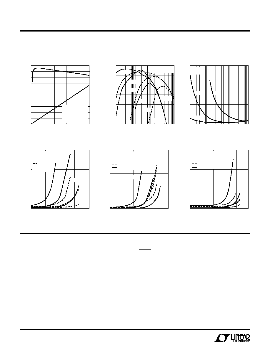
TYPICAL PERFOR
M
A
N
CE CHARACTERISTICS
U
W
Power Conversion Efficiency and
Supply Current vs Load Current
OSCILLATOR FREQUENCY (kHz)
0.1
0
OUTPUT RESISTANCE (
)
2000
3000
1
10
100
LTC1144 · TPC12
1000
1
µ
F
10
µ
F
100
µ
F
T
A
= 25°C
V
+
= 15V
OSCILLATOR FREQUENCY (kHz)
0.1
70
POWER CONVERSION EFFICIENCY (%)
90
95
100
1
10
100
LTC1144 · TPC11
85
80
75
T
A
= 25°C, V
+
= 15V
BOOST = OPEN
I
L
= 20mA
I
L
= 3mA
1
µ
F
1
µ
F
10
µ
F
10
µ
F
100
µ
F
100
µ
F
Power Conversion Efficiency
vs Oscillator Frequency
Output Resistance
vs Oscillator Frequency
Output Voltage vs Load Current
LOAD CURRENT (mA)
10
OUTPUT VOLTAGE (V)
5
0
0.001
0.1
1
100
LTC1144 · TPC15
15
0.01
10
V
+
= 15V
T
A
= 25°C
C1 = C2
BOOST = 15V
0.1
µ
F
0.1
µ
F
1
µ
F
1
µ
F
10
µ
F
10
µ
F
BOOST = OPEN
Output Voltage vs Load Current
LOAD CURRENT (mA)
4
OUTPUT VOLTAGE (V)
3
2
1
0
0.001
0.1
1
100
LTC1144 · G14
5
0.01
10
0.1
µ
F
0.1
µ
F 10
µ
F
10
µ
F
1
µ
F
1
µ
F
V
+
= 5V
T
A
= 25°C
C1 = C2
BOOST = 5V
BOOST = OPEN
LOAD CURRENT (mA)
0.01
0
RIPPLE VOLTAGE (mV)
500
1000
1
µ
F
1
µ
F
1500
0.1
1
LTC1144 · TPC13
10
100
0.1
µ
F
10
µ
F
10
µ
F
V
+
= 5V
T
A
= 25°C
C1 = C2
BOOST = 5V
BOOST =
OPEN
0.1
µ
F
Ripple Voltage vs Load Current
PI FU CTIO S
U
U
U
Boost (Pin 1): This pin will raise the oscillator frequency
by a factor of 10 if tied high.
CAP
+
(Pin 2): Positive Terminal for Pump Capacitor.
GND (Pin 3): Ground Reference.
CAP
(Pin 4): Negative Terminal for Pump Capacitor.
V
OUT
(Pin 5): Output of the Converter.
SHDN (Pin 6): Shutdown Pin. Tie to V
+
pin or leave floating
for normal operation. Tie to ground when in shutdown
mode.
OSC (Pin 7): Oscillator Input Pin. This pin can be overdriven
with an external clock or can be slowed down by connect-
ing an external capacitor between this pin and ground.
V
+
(Pin 8): Input Voltage.
LOAD CURRENT (mA)
0
POWER CONVERSION EFFICIENCY (%)
SUPPLY CURRENT (mA)
60
80
100
16
LTC1144 · TPC10
40
20
0
30
40
50
20
10
0
4
8
12
20
P
EFF
I
S
T
A
= 25°C
V
+
= 5V
C1 = C2 = 10
µ
F
BOOST = OPEN
(SEE TEST CIRCUIT)
5
LTC1144
TEST CIRCUITS
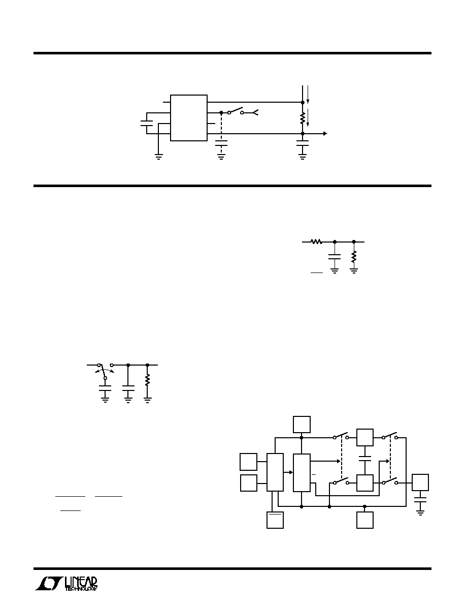
Figure 1.
1
2
3
4
8
7
6
5
+
+
C1
10
µ
F
C2
10
µ
F
I
S
V
OUT
V
+
15V
I
L
R
L
EXTERNAL
OSCILLATOR
C
OSC
1144 F01
LTC1144
U
S
A
O
PPLICATI
W
U
U
I FOR ATIO
Theory of Operation
To understand the theory of operation of the LTC1144, a
review of a basic switched-capacitor building block is
helpful.
In Figure 2, when the switch is in the left position, capacitor
C1 will charge to voltage V1. The total charge on C1 will be
q1 = C1V1. The switch then moves to the right, discharg-
ing C1 to voltage V2. After this discharge time, the charge
on C1 is q2 = C1V2. Note that charge has been transferred
from the source V1 to the output V2. The amount of charge
transferred is:
q = q1 q2 = C1(V1 V2)
V2
R
L
C2
C1
V1
f
1144 F02
Figure 2. Switched-Capacitor Building Block
If the switch is cycled f times per second, the charge
transfer per unit time (i.e., current) is:
I = f
×
q = f
×
C1(V1 V2)
Rewriting in terms of voltage and impedance equivalence,
I
V
V
f C
V
V
R
EQUIV
=
-
×
=
-
1
2
1
1
1
2
A new variable R
EQUIV
has been defined such that R
EQUIV
= 1/(f
×
C1). Thus, the equivalent circuit for the switched-
capacitor network is as shown in Figure 3.
Figure 3. Switched-Capacitor Equivalent Circuit
V2
R
L
R
EQUIV
C2
V1
1144 F03
R
EQUIV
=
1
f
×
C1
Examination of Figure 4 shows that the LTC1144 has the
same switching action as the basic switched-capacitor
building block. With the addition of finite switch on-
resistance and output voltage ripple, the simple theory,
although not exact, provides an intuitive feel for how the
device works.
For example, if you examine power conversion efficiency
as a function of frequency (see Figure 5), this simple
theory will explain how the LTC1144 behaves. The loss,
Figure 4. LTC1144 Switched-Capacitor
Voltage Converter Block Diagram
SHDN
(6)
OSC
(7)
10X
(1)
BOOST
1144 F04
OSC
÷
2
V
+
(8)
SW1
SW2
CAP
+
(2)
CAP
(4)
GND
(3)
V
OUT
(5)
C2
C1
+
+
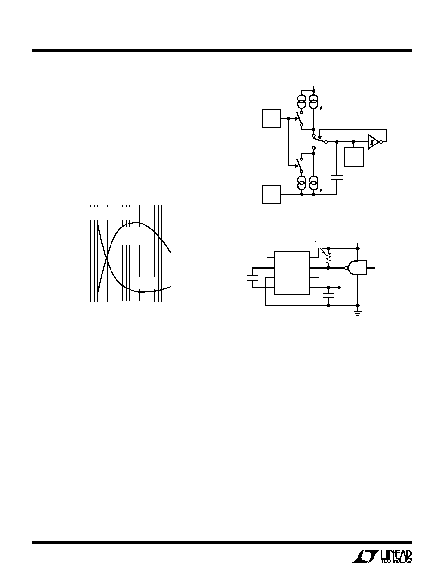
6
LTC1144
and hence the efficiency, is set by the output impedance.
As frequency is decreased, the output impedance will
eventually be dominated by the 1/(f
×
C1) term and power
efficiency will drop.
Note also that power efficiency decreases as frequency
goes up. This is caused by internal switching losses which
occur due to some finite charge being lost on each
switching cycle. This charge loss per unit cycle, when
multiplied by the switching frequency, becomes a current
loss. At high frequency this loss becomes significant and
the power efficiency starts to decrease.
U
S
A
O
PPLICATI
W
U
U
I FOR ATIO
OSCILLATOR FREQUENCY (kHz)
0.1
POWER CONVERSION EFFICIENCY (%)
OUTPUT RESISTANCE (
)
100
95
90
85
80
75
70
600
500
400
300
200
100
0
1
10
100
1144 F05
V
+
= 15V, C1 = C2 = 10
µ
F
I
L
= 20mA, T
A
= 25°C
POWER
CONVERSION
EFFICIENCY
OUTPUT
RESISTANCE
Figure 5. Power Conversion Efficiency and Output
Resistance vs Oscillator Frequency
SHDN (Pin 6)
The LTC1144 has a SHDN pin that will disable the internal
oscillator when it is pulled low. The supply current will also
drop to 8
µ
A.
OSC (Pin 7) and Boost (Pin 1)
The switching frequency can be raised, lowered or driven
from an external source. Figure 6 shows a functional
diagram of the oscillator circuit.
By connecting the boost pin (pin 1) to V
+
, the charge and
discharge current is increased, and hence the frequency is
increased by approximately 10 times. Increasing the fre-
quency will decrease output impedance and ripple for
higher load currents.
Loading pin 7 with more capacitance will lower the fre-
quency. Using the boost (pin 1) in conjunction with exter-
nal capacitance on pin 7 allows user selection of the
frequency over a wide range.
Driving the LTC1144 from an external frequency source
can be easily achieved by driving pin 7 and leaving the
boost pin open as shown in Figure 7. The output current
from pin 7 is small, typically 4
µ
A, so a logic gate is capable
of driving this current. The choice of using a CMOS logic
gate is best because it can operate over a wide supply
voltage range (3V to 15V) and has enough voltage swing
to drive the internal Schmitt trigger shown in Figure 6. For
5V applications, a TTL logic gate can be used by simply
adding an external pull-up resistor (see Figure 7).
Capacitor Selection
External capacitors C1 and C2 are not critical. Matching is
not required, nor do they have to be high quality or tight
tolerance. Aluminum or tantalum electrolytics are excellent
choices, with cost and size being the only consideration.
Figure 6. Oscillator
OSC
(7)
SCHMITT
TRIGGER
BOOST
(1)
1144 F06
9I
9I
I
I
V
+
GND
(3)
20pF
1
2
3
4
8
7
6
5
+
+
C1
OSC INPUT
NC
REQUIRED FOR
TTL LOGIC
C2
100k
(V
+
)
V
+
1144 F07
LTC1144
Figure 7. External Clocking
7
LTC1144
Information furnished by Linear Technology Corporation is believed to be accurate and reliable.
However, no responsibility is assumed for its use. Linear Technology Corporation makes no represen-
tation that the interconnection of its circuits as described herein will not infringe on existing patent rights.
U
S
A
O
PPLICATI
TYPICAL
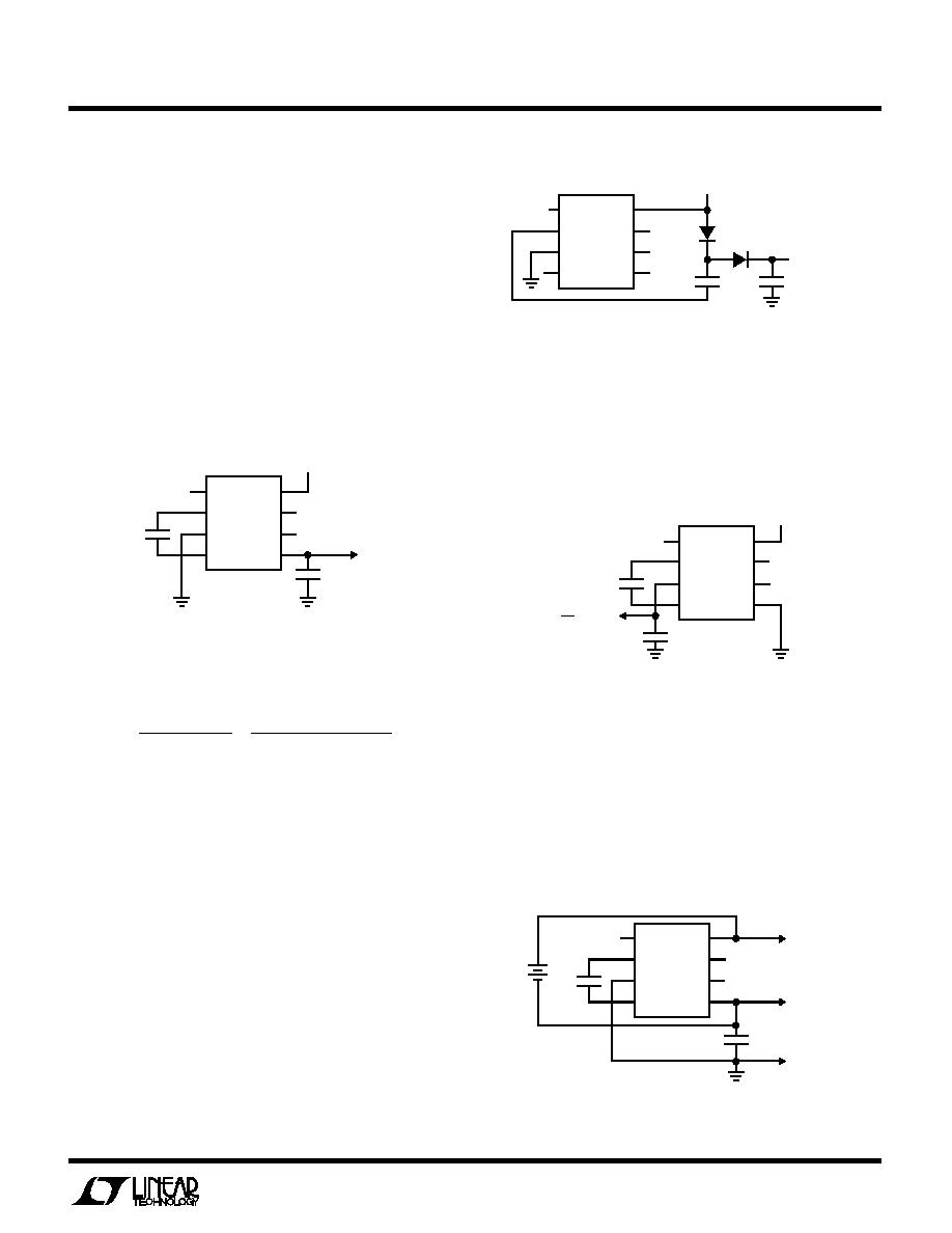
Negative Voltage Converter
Figure 8 shows a typical connection which will provide a
negative supply from an available positive supply. This
circuit operates over full temperature and power supply
ranges
without the need of any external diodes.
The output voltage (pin 5) characteristics of the circuit are
those of a nearly ideal voltage source in series with a 56
resistor. The 56
output impedance is composed of two
terms: 1) the equivalent switched capacitor resistance
(see Theory of Operation), and 2) a term related to the on-
resistance of the MOS switches.
Figure 9. Voltage Doubler
1
2
3
4
8
7
6
5
+
+
+
+
V
IN
2V TO 18V
V
OUT
= 2(V
IN
1)
10
µ
F
10
µ
F
V
d
1N4148
V
d
1N4148
1144 F09
LTC1144
Ultra-Precision Voltage Divider
An ultra-precision voltage divider is shown in Figure 10. To
achieve the 0.0002% accuracy indicated, the load current
should be kept below 100nA. However, with a slight loss
in accuracy, the load current can be increased.
At an oscillator frequency of 10kHz and C1 = 10
µ
F, the first
term is:
R
f
C
EQUIV
OSC
=
( )
×
=
×
×
×
=
-
1
2
1
1
5 10
10 10
20
3
6
/
Notice that the above equation for R
EQUIV
is
not a capaci-
tive reactance equation (X
C
= 1/
C) and does not contain
a 2
term.
The exact expression for output impedance is extremely
complex, but the dominant effect of the capacitor is clearly
shown in Figure 5. For C1 = C2 = 10
µ
F, the output
impedance goes from 56
at f
OSC
= 10kHz to 250
at
f
OSC
= 1kHz. As the 1/(f
×
C) term becomes large compared
to the switch on-resistance term, the output resistance is
determined by 1/(f
×
C) only.
Voltage Doubling
Figure 9 shows a two-diode capacitive voltage doubler.
With a 15V input, the output is 29.45V with no load and
28.18V with a 10mA load.
Figure 8. Negative Voltage Converter
1
2
3
4
8
7
6
5
+
+
10
µ
F
10
µ
F
V
+
2V TO 18V
V
OUT
= V
+
T
MIN
T
A
T
MAX
1144 F08
LTC1144
1
2
3
4
8
7
6
5
+
+
C2
10
µ
F
C1
10
µ
F
V
+
4V TO 36V
1144 F10
LTC1144
±0.002%
T
MIN
T
A
T
MAX
I
L
100nA
V+
2
Figure 10. Ultra-Precision Voltage Divider
Battery Splitter
A common need in many systems is to obtain (+) and ()
supplies from a single battery or single power supply
system. Where current requirements are small, the circuit
shown in Figure 11 is a simple solution. It provides
symmetrical
±
output voltages, both equal to one half the
input voltage. The output voltages are both referenced to
pin 3 (output common).
1
2
3
4
8
7
6
5
+
+
C2
10
µ
F
C1
10
µ
F
OUTPUT
COMMON
V
B
/2
9V
V
B
/2
9V
1144 F11
LTC1144
V
B
18V
+
Figure 11. Battery Splitter
8
LTC1144
U
S
A
O
PPLICATI
TYPICAL
Linear Technology Corporation
1630 McCarthy Blvd., Milpitas, CA 95035-7487
(408) 432-1900
q
FAX
: (408) 434-0507
q
TELEX
: 499-3977
©
LINEAR TECHNOLOGY CORPORATION 1994
LT/GP 0494 10K · PRINTED IN USA
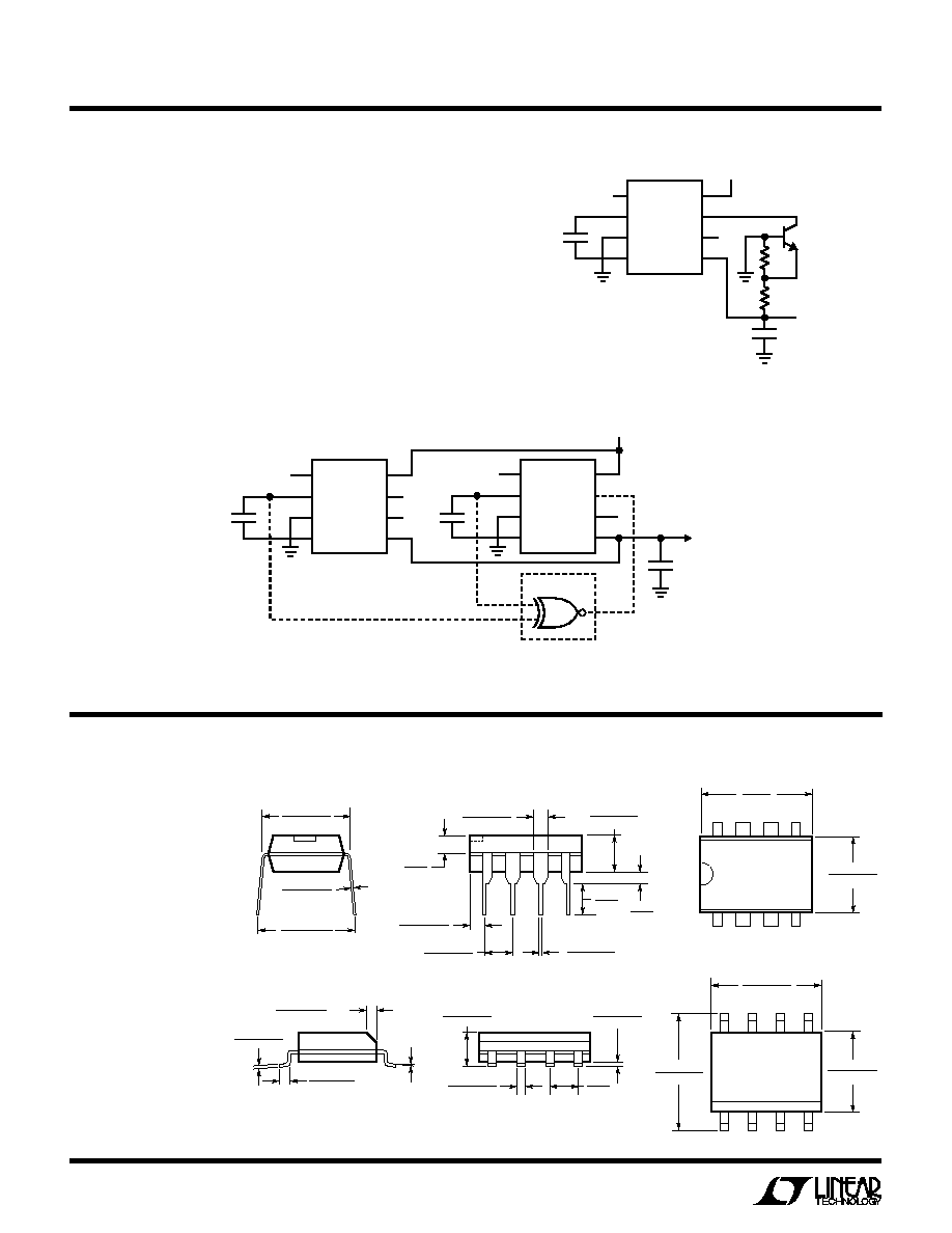
Regulated 5V Output Voltage
Figure 12 shows a regulated 5V output with a 9V input.
With a 0mA to 5mA load current, the R
OUT
is below 20
.
Paralleling for Lower Output Resistance
Additional flexibility of the LTC1144 is shown in Figure 13.
Two LTC1144s are connected in parallel to provide a lower
effective output resistance. However, if the output resis-
tance is dominated by 1/(f
×
C1), increasing the capacitor
size (C1) or increasing the frequency will be of more
benefit than the paralleling circuit shown.
Figure 12. A Regulated 5V Supply
1
2
3
4
8
7
6
5
+
+
1
µ
F
100
µ
F
5V
9V
36k
300k
1144 F12
LTC1144
2N2369
Figure 13. Paralleling for Lower Output Resistance
V
OUT
= (V
+
)
V
+
C1
10
µ
F
C2
20
µ
F
1144 F13
1
2
3
4
8
7
6
5
LTC1144
+
+
C1
10
µ
F
1/4 CD4077*
* THE EXCLUSIVE NOR GATE
SYNCHRONIZES BOTH LTC1144s
TO MINIMIZE RIPPLE
1
2
3
4
8
7
6
5
LTC1144
+
PACKAGE DESCRIPTIO
N
U
Dimemsions in inches (millimeters) unless otherwise noted.
0.009 0.015
(0.229 0.381)
0.300 0.320
(7.620 8.128)
0.325
+0.025
0.015
+0.635
0.381
8.255
(
)
0.045 ± 0.015
(1.143 ± 0.381)
0.100 ± 0.010
(2.540 ± 0.254)
0.065
(1.651)
TYP
0.045 0.065
(1.143 1.651)
0.130 ± 0.005
(3.302 ± 0.127)
0.020
(0.508)
MIN
0.018 ± 0.003
(0.457 ± 0.076)
0.125
(3.175)
MIN
1
2
3
4
8
7
6
5
0.250 ± 0.010
(6.350 ± 0.254)
0.400
(10.160)
MAX
0.016 0.050
0.406 1.270
0.010 0.020
(0.254 0.508)
×
45
°
0° 8° TYP
0.008 0.010
(0.203 0.254)
0.053 0.069
(1.346 1.752)
0.014 0.019
(0.355 0.483)
0.004 0.010
(0.101 0.254)
0.050
(1.270)
BSC
1
2
3
4
0.150 0.157
(3.810 3.988)
8
7
6
5
0.189 0.197
(4.801 5.004)
0.228 0.244
(5.791 6.197)
*THESE DIMENSIONS DO NOT INCLUDE MOLD FLASH OR PROTRUSIONS.
MOLD FLASH OR PROTRUSIONS SHALL NOT EXCEED 0.006 INCH (0.15mm).
S8 Package
8-Lead Plastic SOIC
N8 Package
8-Lead Plastic DIP