Äîêóìåíòàöèÿ è îïèñàíèÿ www.docs.chipfind.ru
1
LTC1046
"Inductorless"
5V to 5V Converter
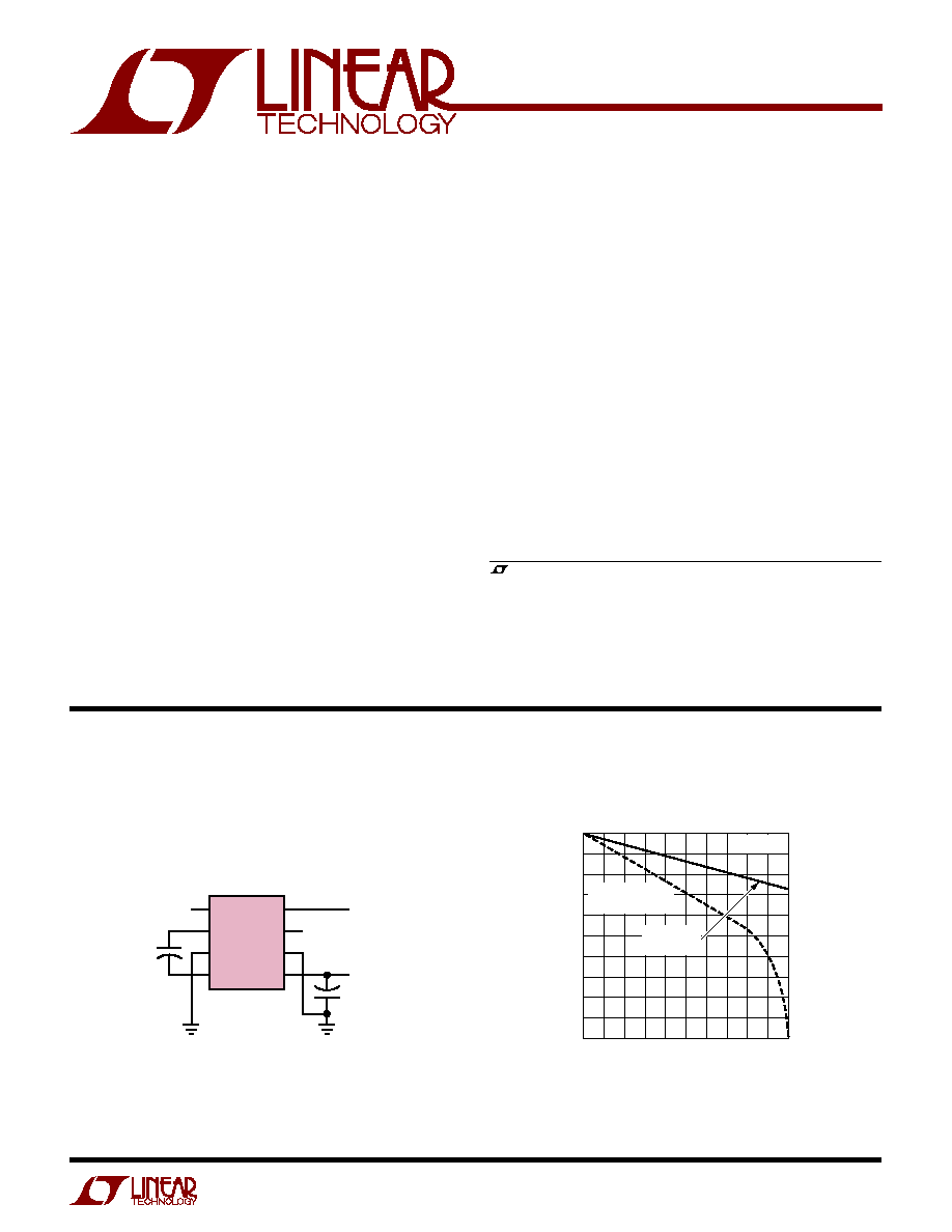
Generating 5V from 5V
Output Voltage vs Load Current for V
+
= 5V
The LTC
®
1046 is a 50mA monolithic CMOS switched
capacitor voltage converter. It plugs in for ICL7660/
LTC1044 in 5V applications where more output current is
needed. The device is optimized to provide high current
capability for input voltages of 6V or less. It trades off
operating voltage to get higher output current. The
LTC1046 provides several voltage conversion functions:
the input voltage can be inverted (V
OUT
= V
IN
), divided
(V
OUT
=V
IN/
2) or multiplied (V
OUT
=
±
nV
IN
).
Designed to be pin-for-pin and functionally compatible
with the ICL7660 and LTC1044, the LTC1046 provides 2.5
times the output drive capability.
s
50mA Output Current
s
Plug-In Compatible with ICL7660/LTC1044
s
R
OUT
= 35
Maximum
s
300
µ
A Maximum
No Load Supply Current at 5V
s
Boost Pin (Pin 1) for Higher Switching Frequency
s
97% Minimum Open-Circuit Voltage Conversion
Efficiency
s
95% Minimum Power Conversion Efficiency
s
Wide Operating Supply Voltage Range: 1.5V to 6V
s
Easy to Use
s
Low Cost
s
Conversion of 5V to
±
5V Supplies
s
Precise Voltage Division, V
OUT
= V
IN
/2
s
Supply Splitter, V
OUT
=
±
V
S
/2
FEATURES
DESCRIPTIO
U
APPLICATIO S
U
TYPICAL APPLICATIO
U
, LTC and LT are registered trademarks of Linear Technology Corporation.
1
2
3
4
8
7
6
5
V
+
OSC
LV
V
OUT
BOOST
CAP
+
GND
CAP
LTC1046
10
µ
F
10
µ
F
1046 TA01
5V INPUT
5V INPUT
+
+
LOAD CURRENT, I
L
(mA)
0
0
OUTPUT VOLTAGE (V)
1
2
3
4
5
10
20
30
40
1046 TA02
50
ICL7660/LTC1044,
R
OUT
= 55
T
A
= 25
°
C
LTC1046,
R
OUT
= 27
LTC1046
2
A
U
G
W
A
W
U
W
A
R
BSOLUTE
XI
TI
S
ORDER PART
NUMBER
ELECTRICAL C
C
HARA TERISTICS
The
q
denotes the specifications which apply over the full operating
temperature range, otherwise specifications are at T
A
= 25
°
C. V
+
= 5V, C
OSC
= 0pF, unless otherwise noted.
LTC1046C
LTC1046I/M
SYMBOL PARAMETER
CONDITIONS
MIN
TYP
MAX
MIN
TYP
MAX
UNITS
I
S
Supply Current
R
L
=
, Pins 1 and 7 No Connection
165
300
165
300
µ
A
R
L
=
, Pins 1 and 7 No Connection,
35
35
µ
A
V
+
= 3V
V
+
L
Minimum Supply Voltage
R
L
= 5k
q
1.5
1.5
V
V
+
H
Maximum Supply Voltage
R
L
= 5k
q
6
6
V
R
OUT
Output Resistance
V
+
= 5V, I
L
= 50mA (Note 3)
27
35
27
35
q
27
45
27
50
V
+
= 2V, I
L
= 10mA
q
60
85
60
90
f
OSC
Oscillator Frequency
V
+
= 5V (Note 4)
20
30
20
30
kHz
V
+
= 2V
4
5.5
4
5.5
kHz
P
EFF
Power Efficiency
R
L
= 2.4k
95
97
95
97
%
V
OUTEFF
Voltage Conversion
R
L
=
97
99.9
97
99.9
%
Efficiency
I
OSC
Oscillator Sink or Source
V
OSC
= 0V or V
+
Current
Pin 1 = 0V
q
4.2
35
4.2
40
µ
A
Pin 1 = V
+
q
15
45
15
50
µ
A
(Note 1)
Supply Voltage ....................................................... 6.5V
Input Voltage on Pins 1, 6 and 7
(Note 2) ............................ 0.3 < V
IN
< (V
+
) + 0.3V
Current into Pin 6 .................................................. 20
µ
A
Output Short Circuit Duration
(V
+
6V) ............................................... Continuous
Operating Temperature Range
LTC1046C .................................... 0
°
C
T
A
70
°
C
LTC1046I ................................. 40
°
C
T
A
85
°
C
LTC1046M .................................... 55
°
C to 125
°
C
Storage Temperature Range ............... 65
°
C to + 150
°
C
Lead Temperature (Soldering, 10 sec.)................. 300
°
C
W
U
U
PACKAGE/ORDER I FOR ATIO
Note 1: Absolute Maximum Ratings are those values beyond which
the life of the device may be impaired.
Note 2: Connecting any input terminal to voltages greater than V
+
or
less than ground may cause destructive latch-up. It is recommended
that no inputs from sources operating from external supplies be
applied prior to power-up of the LTC1046.
Note 3: R
OUT
is measured at T
J
= 25
°
C immediately after power-on.
Note 4: f
OSC
is tested with C
OSC
= 100pF to minimize the effects of test
fixture capacitance loading. The 0pF frequency is correlated to this 100pF
test point, and is intended to simulate the capacitance at pin 7 when the
device is plugged into a test socket and no external capacitor is used.
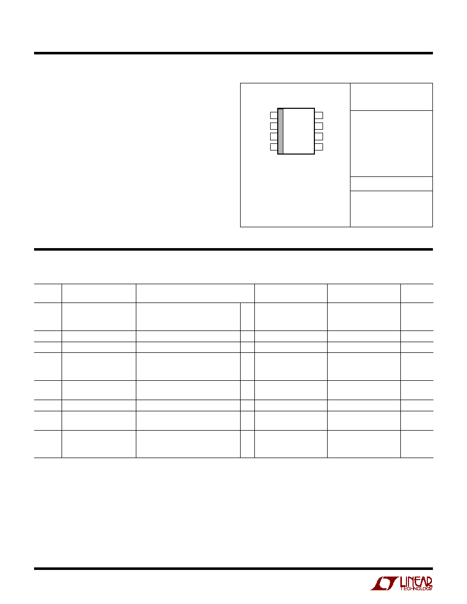
LTC1046CN8
LTC1046CS8
LTC1046IN8
LTC1046IS8
LTC1046MJ8
S8 PART MARKING
1046
1046I
1
2
3
4
8
7
6
5
TOP VIEW
V
+
OSC
LV
V
OUT
BOOST
CAP
+
GND
CAP
J8 PACKAGE
8-LEAD CERDIP
N8 PACKAGE
8-LEAD PDIP
S8 PACKAGE
8-LEAD PLASTIC SO
T
JMAX
= 160
°
C,
JA
= 100
°
C (J8)
T
JMAX
= 110
°
C,
JA
= 130
°
C (N8)
T
JMAX
= 150
°
C,
JA
= 150
°
C (S8)
3
LTC1046
EXTERNAL CAPACITOR (PIN 7 TO GND), C
OSC
(pF)
1
0.1
OSCILLATOR FREQUENCY, f
OSC
(kHz)
1
10
100
10
100
10000
1046 G09
1000
V
+
= 5V
T
A
= 25
°
C
PIN 1 = OPEN
PIN 1 = V
+
LOAD CURRENT, I
L
(mA)
0
2.5
OUTPUT VOLTAGE (V)
2.0
1.5
1.0
0.5
0.0
0.5
2
4
6
8
1046 G07
10 12 14 16 18 20
1.0
1.5
2.0
2.5
SLOPE = 52
T
A
= 25
°
C
V
+
= 2V
f
OSC
= 8kHz
C1 = C2 = 10
µ
F
LOAD CURRENT, I
L
(mA)
0
5
OUTPUT VOLTAGE (V)
4
3
2
1
0
1
10 20 30 40
1046 G08
50 60 70 80 90 100
2
3
4
5
SLOPE = 27
T
A
= 25
°
C
V
+
= 5V
f
OSC
= 30kHz
C1 = C2 = 10
µ
F
OSCILLATOR FREQUENCY, f
OSC
(Hz)
100
80
POWER CONVERSION EFFICIENCY, P
EFF
(%)
86
92
98
100
1k
10k
100k
1M
1046 G06
96
94
90
88
84
82
V
+
= 5V
T
A
= 25
°
C
C1 = C2
A = 100
µ
F, 1mA
B = 100
µ
F, 15mA
C = 10
µ
F, 1mA
D = 10
µ
F, 15mA
E = 1
µ
F, 1mA
F = 1
µ
F, 15mA
A
C
B
E
D
F
LOAD CURRENT, I
L
(mA)
0
30
POWER CONVERSION EFFICIENCY, P
EFF
(%)
50
60
70
80
90
100
30
40
60
70
1046 G05
40
10
20
50
P
EFF
I
S
20
10
0
T
A
= 25
°
C
V
+
= 5V
C1 = C2 = 10
µ
F
f
OSC
= 30kHz
30
50
60
70
80
90
100
40
20
10
0
SUPPLY CURRENT (mA)
LOAD CURRENT, I
L
(mA)
0
30
POWER CONVERSION EFFICIENCY, P
EFF
(%)
50
60
70
80
90
100
3
4
6
7
1046 G04
40
1
2
5
P
EFF
I
S
20
10
0
T
A
= 25
°
C
V
+
= 2V
C1 = C2 = 10
µ
F
f
OSC
= 8kHz
8
9
10
3
5
6
7
8
9
10
4
2
1
0
SUPPLY CURRENT (mA)
AMBIENT TEMPERATURE (
°
C)
55
10
OUTPUT RESISTANCE (
)
30
40
50
60
70
80
25
50
100
125
1046 G03
20
25
0
75
C1 = C2 = 10
µ
F
V
+
= 2V, C
OSC
= 0pF
V
+
= 5V, C
OSC
= 0pF
OSCILLATOR FREQUENCY, f
OSC
(Hz)
100
0
OUTPUT RESISTANCE, R
O
(
)
200
300
400
500
1k
10k
100k
1046 G01
100
T
A
= 25
°
C
V
+
= 5V
I
L
= 10mA
C1 = C2
= 1
µ
F
C1 = C2
= 10
µ
F
C1 = C2
= 100
µ
F
C
C
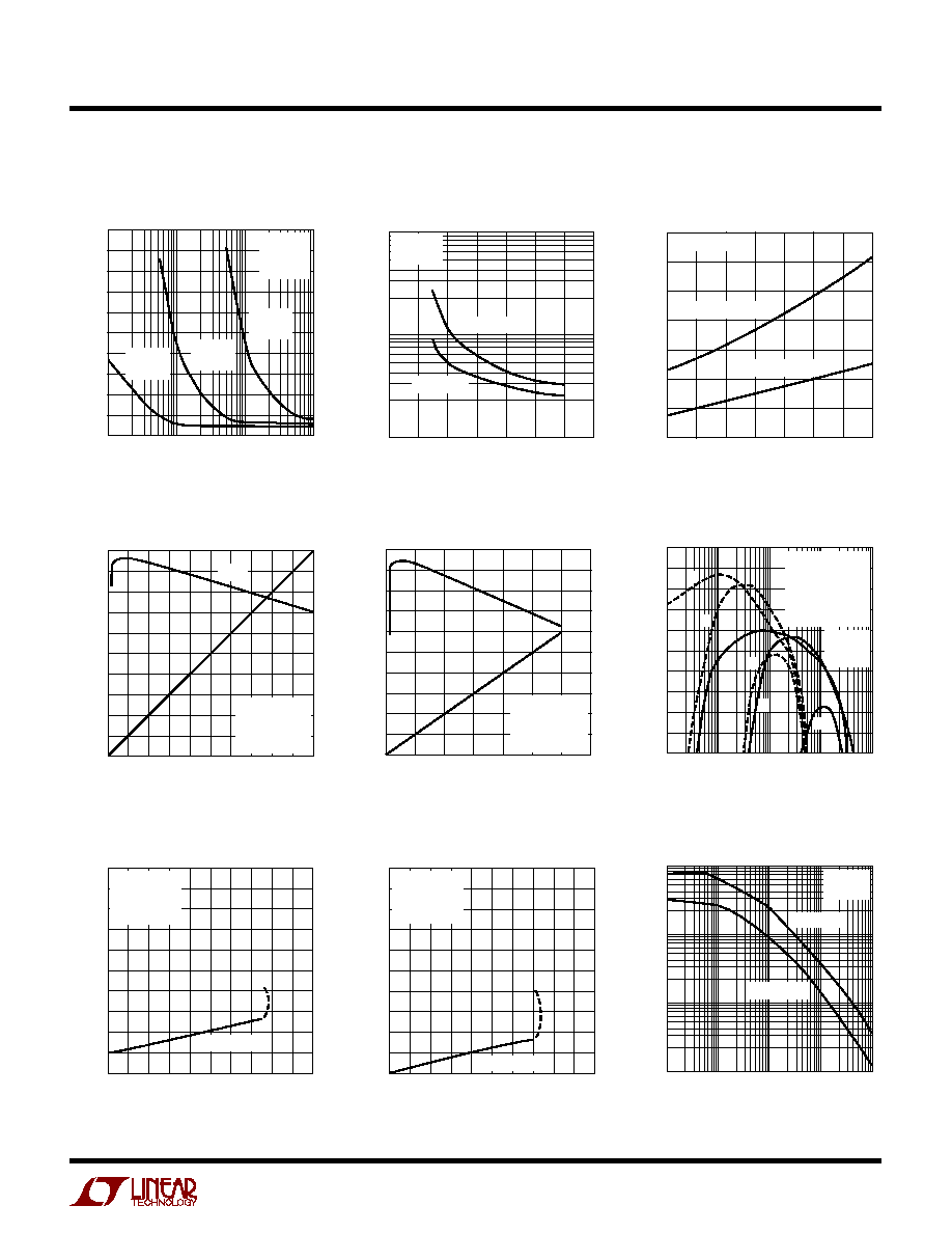
HARA TERISTICS
U
W
A
TYPICAL PERFOR
CE
(Using Test Circuit in Figure 1)
Output Resistance vs
Output Resistance vs
Output Resistance vs
Oscillator Frequency
Supply Voltage
Temperature
Power Conversion Efficiency vs
Power Conversion Efficiency vs
Power Conversion Efficiency vs
Load Current for V
+
= 2V
Load Current for V
+
= 5V
Oscillator Frequency
Output Voltage vs Load Current
Output Voltage vs Load Current
Oscillator Frequency as a
for V
+
= 2V
for V
+
= 5V
Function of C
OSC
SUPPLY VOLTAGE, V
+
(V)
0
10
OUTPUT RESISTANCE, R
O
(
)
100
1000
2
5
6
7
1046 G02
1
3
4
T
A
= 25
°
C
I
L
= 3mA
C
OSC
= 100pF
C
OSC
= 0pF
LTC1046
4
AMBIENT TEMPERATURE (
°
C)
55
26
OSCILLATOR FREQUENCY, f
OSC
(kHz)
30
32
34
36
38
40
25
50
100
125
1046 G11
28
25
0
75
V
+
= 5V
C
OSC
= 0pF
AMBIENT TEMPERATURE (
°
C)
0
1
OSCILLATOR FREQUENCY, f
OSC
(kHz)
10
100
1
4
5
7
1046 G10
2
3
6
T
A
= 25
°
C
C
OSC
= 0pF
C
C
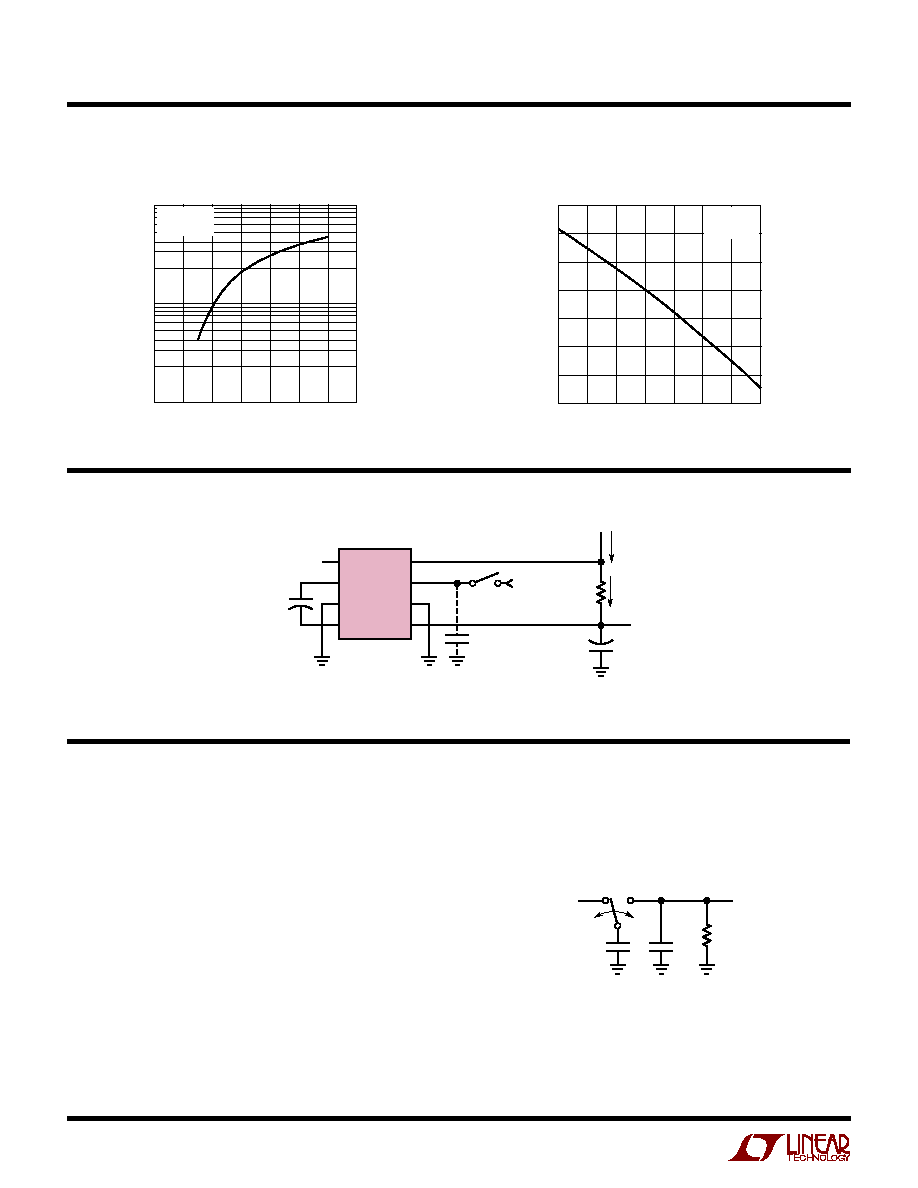
HARA TERISTICS
U
W
A
TYPICAL PERFOR
CE
TEST CIRCUIT
Figure 1
U
S
A
O
PPLICATI
W
U
U
I FOR ATIO
Theory of Operation
To understand the theory of operation of the LTC1046, a
review of a basic switched capacitor building block is
helpful.
In Figure 2, when the switch is in the left position, capacitor
C1 will charge to voltage V1. The total charge on C1 will be
q1 = C1V1. The switch then moves to the right, discharg-
ing C1 to voltage V2. After this discharge time, the charge
on C1 is q2 = C1V2. Note that charge has been transferred
from the source, V1, to the output, V2. The amount of
charge transferred is:
q = q1 q2 = C1(V1 V2).
If the switch is cycled "f" times per second, the charge
transfer per unit time (i.e., current) is:
I = f ·
q = f · C1(V1 V2).
Figure 2. Switched Capacitor Building Block
Oscillator Frequency as a
Oscillator Frequency vs
Function of Supply Voltage
Temperature
(Using Test Circuit in Figure 1)
C
OSC
EXTERNAL
OSCILLATOR
C2
10
µ
F
V
OUT
V
+
(5V)
R
L
I
S
I
L
1046 F01
1
2
3
4
8
7
6
5
V
+
OSC
LV
V
OUT
BOOST
CAP
+
GND
CAP
LTC1046
C1
10
µ
F
+
+
C1
f
C2
1046 F02
V2
V1
R
L
5
LTC1046
U
S
A
O
PPLICATI
W
U
U
I FOR ATIO
Rewriting in terms of voltage and impedance equivalence,
I
V
V
fC
V
V
R
EQUIV
=
( )
=
1
2
1
1
1
2
/
.
A new variable, R
EQUIV
, has been defined such that
R
EQUIV
= 1/fC1. Thus, the equivalent circuit for the switched
capacitor network is as shown in Figure 3.
As frequency is decreased, the output impedance will
eventually be dominated by the 1/fC1 term and power
efficiency will drop. The typical curves for power effi-
ciency versus frequency show this effect for various capaci-
tor values.
Note also that power efficiency decreases as frequency
goes up. This is caused by internal switching losses which
occur due to some finite charge being lost on each
switching cycle. This charge loss per unit cycle, when
multiplied by the switching frequency, becomes a current
loss. At high frequency this loss becomes significant and
the power efficiency starts to decrease.
LV (Pin 6)
The internal logic of the LTC1046 runs between V
+
and LV
(Pin 6). For V
+
greater than or equal to 3V, an internal
switch shorts LV to GND (Pin 3). For V
+
less than 3V, the
LV pin should be tied to ground. For V
+
greater than or
equal to 3V, the LV pin can be tied to ground or left floating.
OSC (Pin 7) and BOOST (Pin 1)
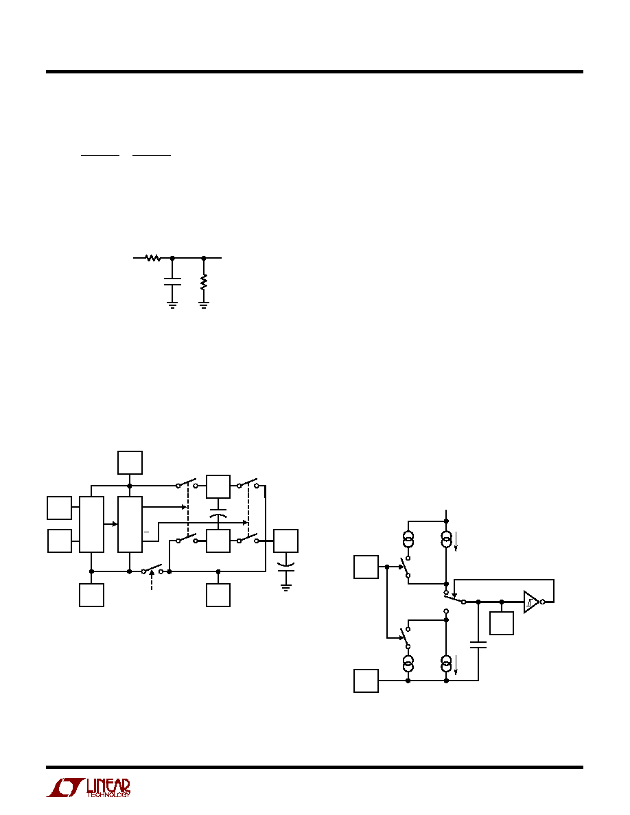
The switching frequency can be raised, lowered or driven
from an external source. Figure 5 shows a functional
diagram of the oscillator circuit.
Figure 3. Switched Capacitor Equivalent Circuit
Figure 4. LTC1046 Switched Capacitor
Voltage Converter Block Diagram
Figure 5. Oscillator
Examination of Figure 4 shows that the LTC1046 has the
same switching action as the basic switched capacitor
building block. With the addition of finite switch ON
resistance and output voltage ripple, the simple theory,
although not exact, provides an intuitive feel for how the
device works.
For example, if you examine power conversion efficiency
as a function of frequency (see typical curve), this simple
theory will explain how the LTC1046 behaves. The loss,
and hence the efficiency, is set by the output impedance.
C2
R
EQUIV
=
1046 F03
V2
V1
R
L
R
EQUIV
1
fC1
1046 F04
CAP+
(2)
CAP
(4)
GND
(3)
V
OUT
(5)
V
+
(8)
LV
(6)
3x
(1)
OSC
(7)
OSC
+2
CLOSED WHEN
V
+
> 3.0V
C1
C2
BOOST
SW1
SW2
+
+
OSC
(7)
1046 F05
LV
(6)
BOOST
(1)
14pF
I
2I
I
2I
V
+
SCHMITT
TRIGGER