3493f.p65
1
LT3493
3493f
APPLICATIO S
U
FEATURES
TYPICAL APPLICATIO
U
DESCRIPTIO
U
1.2A, 750kHz Step-Down
Switching Regulator in
2mm
× 3mm DFN
The LT
®
3493 is a current mode PWM step-down DC/DC
converter with an internal 1.75A power switch. The wide
operating input range of 3.6V to 36V (40V maximum) makes
the LT3493 ideal for regulating power from a wide variety
of sources, including unregulated wall transformers, 24V
industrial supplies and automotive batteries. Its high op-
erating frequency allows the use of tiny, low cost inductors
and ceramic capacitors, resulting in low, predictable out-
put ripple.
Cycle-by-cycle current limit provides protection against
shorted outputs and soft-start eliminates input current
surge during start-up. The low current (<2
µA) shutdown
mode provides output disconnect, enabling easy power
management in battery-powered systems.
Wide Input Range: 3.6V to 36V Operating,
40V Maximum
1.2A Output Current
Fixed Frequency Operation: 750kHz
Output Adjustable Down to 780mV
Short-Circuit Robust
Uses Tiny Capacitors and Inductors
Soft-Start
Internally Compensated
Low Shutdown Current: <2
µA
Low V
CESAT
Switch: 330mV at 1A
Thermally Enhanced, Low Profile DFN Package
Automotive Battery Regulation
Industrial Control Supplies
Wall Transformer Regulation
Distributed Supply Regulation
Battery-Powered Equipment
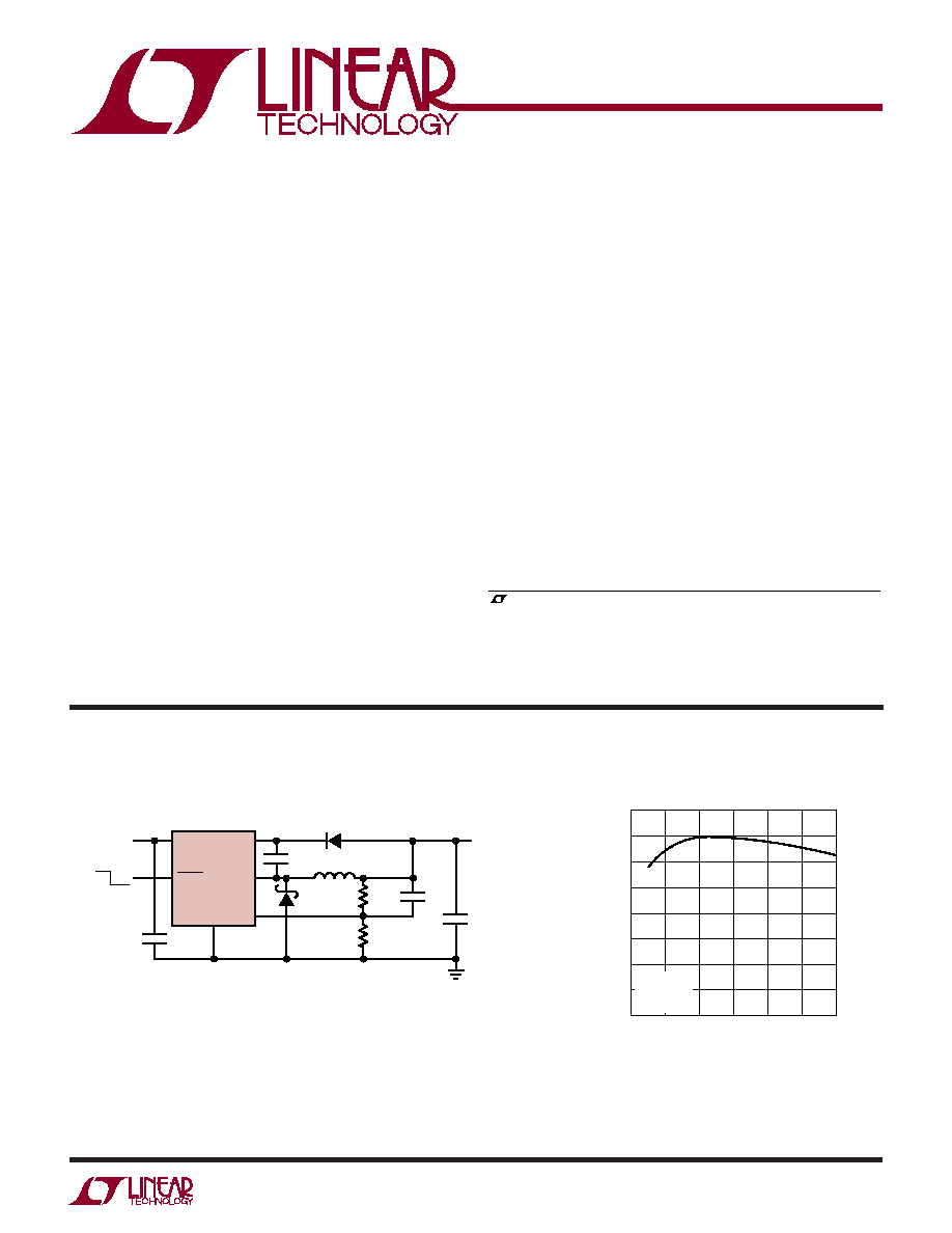
3.3V Step-Down Converter
Efficiency
V
IN
4.2V TO 36V
ON OFF
0.1
µF
10
µH
32.4k
10
µF
3493 TA01a
22pF
1
µF
10k
V
OUT
3.3V
1.2A, V
IN
> 12V
0.95A, V
IN
> 5V
V
IN
BOOST
GND
FB
SHDN
SW
LT3493
, LTC and LT are registered trademarks of Linear Technology Corporation.
ThinSOT is a trademark of Linear Technology Corporation.
All other trademarks are the property of their respective owners.
LOAD CURRENT (A)
EFFICIENCY (%)
70
80
3493 TA01b
60
50
0.4
0.8
1.2
0.2
0
0.6
1.0
90
65
75
55
85
V
IN
= 12V
V
OUT
= 3.3V
L = 10
µH
2
LT3493
3493f
Input Voltage (V
IN
) .................................................. 40V
BOOST Pin Voltage .................................................. 50V
BOOST Pin Above SW Pin ....................................... 25V
SHDN Pin ................................................................ 40V
FB Voltage ................................................................. 6V
Operating Temperature Range (Note 2)
LT3493E .............................................. 40
°C to 85°C
LT3493I ............................................ 40
°C to 125°C
Maximum Junction Temperature .......................... 125
°C
Storage Temperature Range ................. 65
°C to 150°C
ORDER PART NUMBER
DCB PART MARKING
LT3493EDCB
LT3493IDCB
ABSOLUTE AXI U RATI GS
W
W
W
U
PACKAGE/ORDER I FOR ATIO
U
U
W
(Note 1)
T
JMAX
= 125
°C,
JA
= 64
°C/ W
EXPOSED PAD (PIN 7) IS GND, MUST BE SOLDERED TO PCB
Order Options Tape and Reel: Add #TR Lead Free: Add #PBF
Lead Free Tape and Reel: Add #TRPBF
Lead Free Part Marking:
http://www.linear.com/leadfree/
PARAMETER
CONDITIONS
MIN
TYP
MAX
UNITS
V
IN
Operating Range
3.6
36
V
Undervoltage Lockout
3.1
3.4
3.6
V
Feedback Voltage
765
780
795
mV
FB Pin Bias Current
V
FB
= Measured V
REF
+ 10mV (Note 4)
50
150
nA
Quiescent Current
Not Switching
1.9
2.5
mA
Quiescent Current in Shutdown
V
SHDN
= 0V
0.01
2
µA
Reference Line Regulation
V
IN
= 5V to 36V
0.007
%/V
Switching Frequency
V
FB
= 0.7V
685
750
815
kHz
V
FB
= 0V
36
kHz
Maximum Duty Cycle
88
95
%
T
A
= 25
°C
91
95
%
The
denotes specifications which apply over the full operating temperature range, otherwise specifications are at T
A
= 25
°C.
V
IN
= 12V, V
BOOST
= 17V, unless otherwise noted. (Note 2)
ELECTRICAL CHARACTERISTICS
Consult LTC Marketing for parts specified with wider operating temperature ranges.
LCGG
LCGH
TOP VIEW
SHDN
V
IN
SW
FB
GND
BOOST
DCB PACKAGE
6-LEAD (2mm
× 3mm) PLASTIC DFN
4
5
7
6
3
2
1
3
LT3493
3493f
PARAMETER
CONDITIONS
MIN
TYP
MAX
UNITS
Switch Current Limit
(Note 3)
1.4
1.75
2.2
A
Switch V
CESAT
I
SW
= 1A
330
mV
Switch Leakage Current
2
µA
Minimum Boost Voltage Above Switch
I
SW
= 1A
1.85
2.2
V
BOOST Pin Current
I
SW
= 1A
30
50
mA
SHDN Input Voltage High
2.3
V
SHDN Input Voltage Low
0.3
V
SHDN Bias Current
V
SHDN
= 2.3V (Note 5)
6
15
µA
V
SHDN
= 0V
0.01
0.1
µA
The
denotes specifications which apply over the full operating temperature range, otherwise specifications are at T
A
= 25
°C.
V
IN
= 12V, V
BOOST
= 17V, unless otherwise noted. (Note 2)
ELECTRICAL CHARACTERISTICS
Note 1: Stresses beyond those listed under Absolute Maximum Ratings
may cause permanent damage to the device. Exposure to any Absolute
Maximum Rating condition for extended periods may affect device
reliability and lifetime.
Note 2: The LT3493E is guaranteed to meet performance specifications
from 0
°C to 85°C. Specifications over the 40°C to 85°C operating
temperature range are assured by design, characterization and correlation
with statistical process controls. The LT3493I specifications are guaran-
teed over the 40
°C to 125°C temperature range.
Note 3: Current limit guaranteed by design and/or correlation to static test.
Slope compensation reduces current limit at higher duty cycle.
Note 4: Current flows out of pin.
Note 5: Current flows into pin.
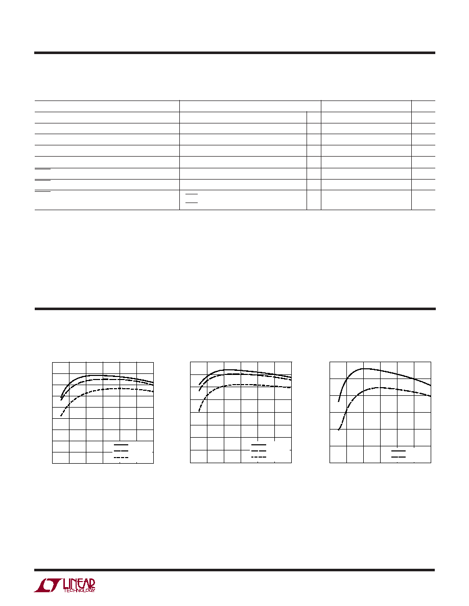
TYPICAL PERFOR A CE CHARACTERISTICS
U
W
Efficiency (V
OUT
= 5V, L = 10
µH)
Efficiency (V
OUT
= 3.3V, L = 10
µH)
Efficiency (V
OUT
= 1.8V, L = 4.7
µH)
LOAD CURRENT (A)
0
50
EFFICIENCY (%)
55
65
70
75
0.8
1.0
95
3493 G01
60
0.2
0.4
0.6
1.2
80
85
90
V
IN
= 8V
V
IN
= 12V
V
IN
= 24V
LOAD CURRENT (A)
0
50
EFFICIENCY (%)
55
65
70
75
0.8
1.0
3493 G02
60
0.2
0.4
0.6
1.2
80
85
90
V
IN
= 8V
V
IN
= 12V
V
IN
= 24V
LOAD CURRENT (A)
0
50
EFFICIENCY (%)
55
65
70
75
0.8
1.0
3493 G03
60
0.2
0.4
0.6
1.2
80
V
IN
= 5V
V
IN
= 12V
T
A
= 25
°C unless otherwise noted.
4
LT3493
3493f
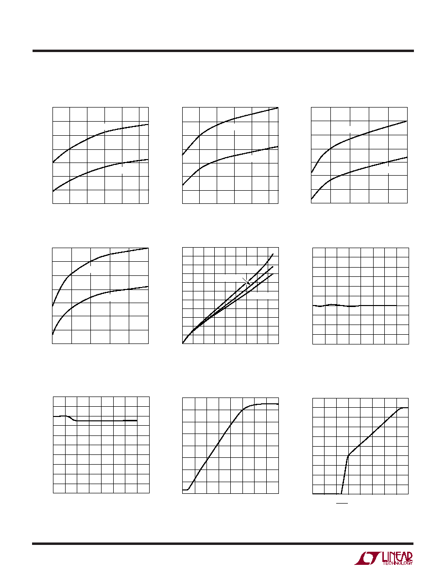
TYPICAL PERFOR A CE CHARACTERISTICS
U
W
Maximum Load Current,
V
OUT
= 5V, L = 8.2
µH
Switch Voltage Drop
Undervoltage Lockout
Maximum Load Current,
V
OUT
= 3.3V, L = 4.7
µH
Switching Frequency
Frequency Foldback
V
IN
(V)
8
1.60
1.50
1.40
1.30
1.20
1.10
1.00
0.90
20
28
3493 G04
12
16
24
OUTPUT CURRENT (A)
TYPICAL
MINIMUM
V
IN
(V)
5
1.40
1.50
1.60
25
3493 G05
1.30
1.20
10
15
20
30
1.10
1.00
0.90
OUTPUT CURRENT (A)
TYPICAL
MINIMUM
SWITCH CURRENT (A)
0
V
CE(SW)
(mV)
150
450
500
550
0.4
0.8 1.0
3493 G06
50
350
250
100
400
0
300
200
0.2
0.6
1.4
1.2
1.6 1.8
T
A
= 25
°C
T
A
= 85
°C
T
A
= 40
°C
TEMPERATURE (
°C)
UVLO (V)
3.60
3.80
4.00
125
3493 G08
3.40
3.20
3.50
3.70
3.90
3.30
3.10
3.00
25
50
25
0
75
100
150
50
TEMPERATURE (
°C)
FREQUENCY (kHz)
720
760
800
125
3493 G09
680
640
700
740
780
660
620
600
25
50
25
0
75
100
150
50
Soft-Start
SHDN PIN VOLTAGE (V)
0
0
SWITCH CURRENT LIMIT (A)
0.2
0.6
0.8
1.0
2.0
1.4
0.50
1
1.25
3493 G13
0.4
1.6
1.8
1.2
0.25
0.75
1.50 1.75
2
FEEDBACK VOLTAGE (mV)
0
SWITCHING FREQUENCY (kHz)
400
600
800
3493 G11
200
0
200
400
600
100
300
500
700
800
300
500
100
700
V
IN
(V)
8
1.60
1.50
1.40
1.30
1.20
1.10
1.00
0.90
20
28
3493 G22
12
16
24
OUTPUT CURRENT (A)
TYPICAL
MINIMUM
Maximum Load Current,
V
OUT
= 5V, L = 33
µH
V
IN
(V)
5
1.40
1.50
1.60
25
3493 G21
1.30
1.20
10
15
20
30
1.10
1.00
0.90
OUTPUT CURRENT (A)
TYPICAL
MINIMUM
Maximum Load Current,
V
OUT
= 3.3V, L = 10
µH
T
A
= 25
°C unless otherwise noted.
5
LT3493
3493f
TYPICAL PERFOR A CE CHARACTERISTICS
U
W
Typical Minimum Input Voltage
(V
OUT
= 5V)
Typical Minimum Input Voltage
(V
OUT
= 3.3V)
Switch Current Limit
Switch Current Limit
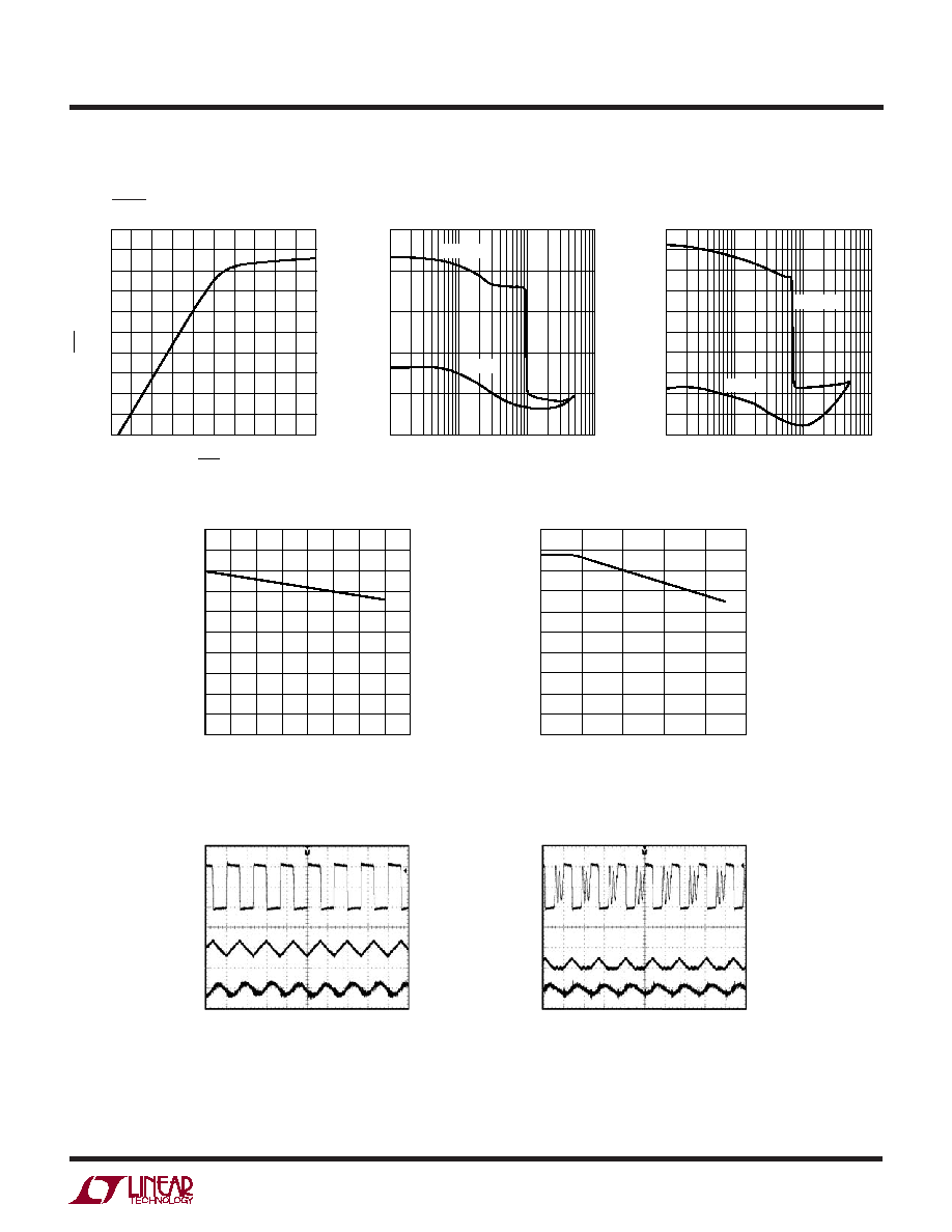
Operating Waveforms
Operating Waveforms,
Discontinuous Mode
I
OUT
(mA)
1
5.0
V
IN
(V)
6.5
7.0
7.5
10
100
1000
3493 G15
6.0
5.5
TO START
TO RUN
I
OUT
(mA)
1
4.3
V
IN
(V)
4.5
4.7
4.9
5.1
10
100
1000
3493 G16
4.1
3.9
3.7
3.5
5.3
5.5
TO START
TO RUN
TEMPERATURE (
°C)
50
1.0
SWITCH CURRENT LIMIT (A)
1.1
1.3
1.4
1.5
2.0
1.7
0
25
100 125 150
3493 G17
1.2
1.8
1.9
1.6
25
50
75
DUTY CYCLE (%)
0
SWITCH CURRENT LIMIT (A)
1.2
1.6
2.0
80
3493 G18
0.8
0.4
1.0
1.4
1.8
0.6
0.2
0
20
40
60
100
SHDN Pin Current
V
SHDN
(V)
0
I
SHDN
(
µ
A)
30
40
50
16
3493 G14
20
10
25
35
45
15
5
0
4
2
8
6
12 14
18
10
20
V
SW
5V/DIV
I
L
0.5A/DIV
0
V
OUT
20mV/DIV
V
IN
= 12V
V
OUT
= 3.3V
I
OUT
= 0.5A
L = 10
µH
C
OUT
= 10
µF
1
µs/DIV
3493 G19
V
SW
5V/DIV
I
L
0.5A/DIV
0
V
OUT
20mV/DIV
1
µs/DIV
3493 G20
V
IN
= 12V
V
OUT
= 3.3V
I
OUT
= 50mA
L = 10
µH
C
OUT
= 10
µF
T
A
= 25
°C unless otherwise noted.