
1
LT1508
Power Factor and PWM
Controller (Voltage Mode)
, LTC and LT are registered trademarks of Linear Technology Corporation.
s
PFC and PWM Single Chip Solution
s
Synchronized Operation up to 300kHz
s
99% Power Factor Over 20:1 Load Current Range
s
Voltage Mode PWM
s
Instantaneous Overvoltage Protection
s
Dedicated Overvoltage Protection (OVP Pin)
s
Minimal Line Current Dead Zone
s
Typical 250
µ
A Start-Up Supply Current
s
Line Switching Noise Filter
s
Low Quiescent Current: 13mA
s
Fast 1.5A Peak Current Gate Drivers
s
Separate Soft Start Control
FEATURES
DESCRIPTIO
N
U
APPLICATIO
N
S
U
s
Universal Power Factor Corrected Power Supplies
and Preregulators
The LT
®
1508 is a complete solution for universal off-line
switching power supplies utilizing active power factor
correction. The PFC section is identical to the LT1248 PFC
controller except the EN/SYNC pin is removed because
PFC and PWM are synchronized internally.
The voltage mode PWM section (LT1509 is the current
mode counterpart) contains all the primary side functions
to convert the PFC preregulated high voltage output to an
isolated low voltage output. The PWM duty cycle is
internally limited to 47% (maximum 50%) to prevent
transformer saturation. PWM soft start begins when the
PFC output reaches the preset voltage. In the event of brief
line loss, PWM will be shut off when the PFC output
voltage drops below 73% of the preset value.
+
+
+
11
16
13
+
+
+
I
M
=
I
A
2
I
B
200
µ
A
2
4
15
19
18
1508 BD
V
SENSE
7.5V
7.9V
V
CC
16V TO 10V
14
µ
A
14
µ
A
7
µ
A
7V TO
4.7V
+
EA
CA
+
CL
2.2V
M1
I
A
I
M
I
B
25k
1V
R
2R
14
VA
OUT
10
V
REF
7.5V
V
REF
12
M
OUT
8
I
SENSE
7
CA
OUT
6
C
SET
R
SET
I
LIM
V
C
50
µ
A
RUN
RUN
R
R
Q
S
S
R
Q
R
OSC
55%
DELAY
200ns
BLANKING
PK
LIM
5
GND1
3
V
CC
17
GTDR1
16V
16V
1
GND2
2
GTDR2
20
I
AC
9
OVP
SS1
SS2
PWMOK
0.7V
+
+
NOTE: PWM PULSE IS DELAYED BY 55% DUTY CYCLE
AFTER PFC PULSE
+
+
BLOCK DIAGRA
M
W

2
LT1508
By using fixed high frequency PWM current averaging
without the need for slope compensation, the LT1508
achieves far lower line current distortion with a smaller
magnetic element than systems that use either peak
current detection, or zero current switching approach, in
both continuous and discontinuous modes of operation.
The LT1508 also provides filtering capability to reject line
DESCRIPTIO
N
U
switching noise which can cause instability when fed into
the multiplier. Line current dead zone is minimized with
low bias voltage at the current input to the multiplier. The
LT1508 provides many protection features including peak
current limiting and overvoltage protection. Implemented
with a very high speed process, the LT1508 can be
operated at frequencies as high as 300kHz.
ABSOLUTE
M
AXI
M
U
M
RATINGS
W
W
W
U
Supply Voltage ........................................................ 27V
GTDR Current Continuous ...................................... 0.5A
GTDR Output Energy ................................................ 5
µ
J
I
AC
, R
SET
, PK
LIM
Input Current .............................. 20mA
V
SENSE
, OVP Input Voltage .................................... V
MAX
I
LIM
, V
C
Input Voltage ................................................ 8V
I
SENSE
, M
OUT
Input Current ...................................
±
5mA
Operating Junction Temperature Range
LT1508C ................................................ 0
°
C to 100
°
C
LT1508I ............................................ 40
°
C to 125
°
C
Thermal Resistance (Junction-to-Ambient)
N Package ................................................... 100
°
C/W
SW Package ................................................ 120
°
C/W
PACKAGE/ORDER I
N
FOR
M
ATIO
N
W
U
U
Consult factory for Military grade parts.
1
2
3
4
5
6
7
8
9
10
TOP VIEW
SW PACKAGE
20-LEAD PLASTIC SO WIDE
N PACKAGE
20-LEAD PDIP
20
19
18
17
16
15
14
13
12
11
GTDR1
GND2
GND1
C
SET
PK
LIM
CA
OUT
I
SENSE
M
OUT
I
AC
VA
OUT
GTDR2
I
LIM
V
C
V
CC
SS1
R
SET
V
SENSE
SS2
V
REF
OVP
T
JMAX
= 125
°
C,
JA
= 100
°
C/ W (N)
T
JMAX
= 125
°
C,
JA
= 120
°
C/ W (SW)
ORDER PART
NUMBER
PARAMETER
CONDITIONS
MIN
TYP
MAX
UNITS
Overall
Supply Current (V
CC
in Undervoltage Lockout)
V
CC
= Lockout Voltage 0.2V
q
0.25
0.45
mA
Supply Current On
11.5V
V
CC
V
MAX
q
13
19
mA
V
CC
Turn-On Threshold (Undervoltage Lockout)
q
15.5
16.5
17.5
V
V
CC
Turn-Off Threshold
q
9.5
10.5
11.5
V
Voltage Amplifier (PFC Section)
Voltage Amp Offset
VA
OUT
= 3.5V
q
10
10
mV
Input Bias Current
V
SENSE
= 0V to 7V
q
25
250
nA
Voltage Gain
70
100
dB
Voltage Amp Unity-Gain Bandwidth
3
MHz
Voltage Amp Output High (Internally Clamped)
q
11.3
13.3
V
Voltage Amp Output Low
q
1.1
2
V
Voltage Amp Short-Circuit Current
VA
OUT
= 0V
q
3
8
17
mA
ELECTRICAL CHARACTERISTICS
Maximum operating voltage (V
MAX
) = 25V, V
CC
= 18V, R
SET
= 15k to GND, C
SET
= 1nF to GND, I
AC
= 100
µ
A, I
SENSE
= 0V, CA
OUT
= 3.5V,
VA
OUT
= 5V, OVP = V
REF
. No load on any outputs unless otherwise noted.
LT1508CN
LT1508CSW
LT1508IN
LT1508ISW

3
LT1508
ELECTRICAL C
C
HARA TERISTICS
PARAMETER
CONDITIONS
MIN
TYP
MAX
UNITS
Current Amplifier (PFC Section)
Current Amp Offset Voltage
q
±
1
±
4
mV
I
SENSE
Bias Current
q
25
250
nA
Current Amp Voltage Gain
80
110
dB
Current Amp Unity-Gain Bandwidth
3
MHz
Current Amp Output High
q
7.2
8.5
V
Current Amp Output Low
q
1.1
2
V
Current Amp Short-Circuit Current
CA
OUT
= 0V
q
3
8
17
mA
Input Range, I
SENSE
, M
OUT
(Linear Operation)
q
0.3
1
V
Reference
Reference Output Voltage
I
REF
= 0mA, T
A
= 25
°
C
7.39
7.50
7.60
V
V
REF
Load Regulation
5mA < I
REF
< 0mA
5
mV
V
REF
Line Regulation
11.5V < V
CC
< V
MAX
q
20
5
20
mV
V
REF
Short-Circuit Current
V
REF
= 0V
q
12
28
50
mA
V
REF
Worst Case
Load, Line, Temperature
q
7.32
7.5
7.68
V
Current Limit
PK
LIM
Offset Voltage
q
25
25
mV
PK
LIM
Input Current
PK
LIM
= 0.1V
q
50
100
µ
A
PK
LIM
to GTDR Propagation Delay
PK
LIM
Falling from 50mV to 50mV
400
ns
Multiplier
Multiplier Output Current
I
AC
= 100
µ
A, R
SET
= 15k
35
µ
A
Multiplier Output Current Offset
R
AC
= 1M from I
AC
to GND
q
0.05
0.5
µ
A
Multiplier Maximum Output Current
I
AC
= 450
µ
A, R
SET
= 15k, VA
OUT
= 7V, M
OUT
= 0V
q
286
260
235
µ
A
Multiplier Gain Constant (Note 1)
0.035
V
2
I
AC
Input Resistance
I
AC
from 50
µ
A to 1mA
15
25
35
k
Oscillator
Oscillator Frequency
R
SET
= 15k, C
SET
= 1000pF
q
85
100
115
kHz
R
SET
= 15k, C
SET
= 1500pF
q
58
68
78
kHz
C
SET
Ramp Peak-to-Peak Amplitude
4.35
4.7
5.0
V
C
SET
Ramp Valley Voltage
1.15
1.3
1.55
V
Overvoltage Comparator (PFC Section)
Comparator Trip Voltage Ratio (V
TRIP
/ V
REF
)
q
1.04
1.05
1.06
Hysteresis
0.35
V
OVP Bias Current
OVP = 7.5V
q
0.2
1
µ
A
OVP Propagation Delay
100
ns
Gate Drivers (GTDR1 and GTDR2)
Max Output Voltage
0mA Load, 18V < V
CC
q
12
15
17.5
V
Output High
200mA Load, 11.5V
V
CC
15V
q
V
CC
3.0
V
Output Low (Device Unpowered)
V
CC
= 0V, 50mA Load (Sinking)
q
0.9
1.5
V
Output Low (Device Active)
200mA Load (Sinking)
q
0.5
1
V
10mA Load
q
0.2
0.4
V
Peak Output Current
10nF from GTDR to GND
2
A
Rise and Fall Time
1nF from GTDR to GND
25
ns
Max Duty Cycle (PFC)
90
96
%
Max Duty Cycle (PWM) (Note 2)
44
50
%
Maximum operating voltage (V
MAX
) = 25V, V
CC
= 18V, R
SET
= 15k to GND, C
SET
= 1nF to GND, I
AC
= 100
µ
A, I
SENSE
= 0V, CA
OUT
= 3.5V,
VA
OUT
= 5V, OVP = V
REF
. No load on any outputs unless otherwise noted.

4
LT1508
I
M
I
AC
(VA
OUT
2)
2
The
q
denotes specifications which apply over the full operating
temperature range.
Note 1: Multiplier Gain Constant: K =
Note 2: GTDR2 (PWM) pulse is delayed by 53% duty cycle after GTDR1
(PFC) is set. See PFC/PWM Synchronization graph in the Typical
Performance Characteristics section.
TYPICAL PERFOR
M
A
N
CE CHARACTERISTICS
U
W
PFC Voltage Amplifier Open-Loop
Gain and Phase
FREQUENCY (Hz)
10
GAIN (dB)
100
80
60
40
20
0
20
100
1k
10k
100k
1508 G01
1M
10M
0
20
40
60
80
100
120
PHASE (DEG)
PHASE
GAIN
FREQUENCY (Hz)
10
GAIN (dB)
100
80
60
40
20
0
20
100
1k
10k
100k
1508 G02
1M
10M
0
20
40
60
80
100
120
PHASE (DEG)
PHASE
GAIN
PFC Current Amplifier Open-Loop
Gain and Phase
TIME
1508 G03
PFC (GTDR1)
53%
PWM (GTDR2)
PFC/PWM Synchronization
ELECTRICAL C
C
HARA TERISTICS
V
CC
= 18V, R
SET
= 15k to GND, C
SET
= 1nF to GND, I
AC
= 100
µ
A, I
SENSE
= 0V, CA
OUT
= 3.5V, VA
OUT
= 5V, OVP = V
REF
. No load on any
outputs, unless otherwise noted.
PARAMETER
CONDITIONS
MIN
TYP
MAX
UNITS
Soft Start Current
SS1 Current (PFC)
SS1 = 2.5V
q
5
12
30
µ
A
SS2 Current (PWM)
SS2 = 1V
q
5
12
30
µ
A
Comparators in PWM Section
I
LIM
Input Current
I
LIM
= 0V, V
C
= 1.6V
q
0.3
2
µ
A
Current Limit Comparator (CL) Threshold
V
C
> 2.6V
q
0.95
1.1
1.20
V
GTDR2 Switching Off Threshold at V
C
or at SS2
I
LIM
= 0V
q
1
V
V
C
Input Current
V
C
= 0V
q
20
80
µ
A
PWMOK Comparator Low Threshold (in Terms of V
REF
)
q
0.57
0.63
0.70
V
C
Pin High Voltage
1mA into V
C
Pin
q
6.2
6.9
7.5
V
GTDR2 Turn-On Blanking Time
180
ns

5
LT1508
TYPICAL PERFOR
M
A
N
CE CHARACTERISTICS
U
W
Reference Voltage
vs Temperature
Supply Current vs Supply Voltage
GTDR Rise and Fall Time
Start-Up Supply Current
vs Supply Voltage
M
OUT
Pin Characteristics
Frequency vs R
SET
and C
SET
GTDR1 Maximum Duty Cycle
vs R
SET
and C
SET
Multiplier Current
JUNCTION TEMPERATURE (
°
C)
75
REFERENCE VOLTAGE (V)
75
7.536
7.524
7.512
7.500
7.488
7.476
7.464
7.452
7.440
7.428
1508 G04
50
150
25
0
25
50
100 125
I
AC
(
µ
A)
0
I
M
(
µ
A)
300
150
0
1508 G05
250
500
VA
OUT
= 7V
VA
OUT
= 6.5V
VA
OUT
= 6V
VA
OUT
= 5.5V
VA
OUT
= 5V
VA
OUT
= 4.5V
VA
OUT
= 4V
VA
OUT
= 3.5V
VA
OUT
= 3V
VA
OUT
= 2.5V
SUPPLY VOLTAGE (V)
10
SUPPLY CURRENT (mA)
16
15
14
13
12
11
10
9
8
7
6
5
1508 G06
21
32
T
J
= 25
°
C
T
J
= 125
°
C
T
J
= 55
°
C
LOAD CAPACITANCE (nF)
0
TIME (ns)
400
300
200
100
0
10
20
30
40
1508 G07
50
RISE TIME
NOTE: GTDR SLEWS
BETWEEN 1V AND 16V
FALL TIME
SUPPLY VOLTAGE (V)
0
SUPPLY CURRENT (
µ
A)
550
500
450
400
350
300
250
200
150
100
50
0
1508 G08
20
125
°
C
55
°
C
25
°
C
4
8
12
16
2
6
10
14
18
C
SET
CAPACITANCE (pF)
200
FREQUENCY (kHz)
500
450
400
350
300
250
200
150
100
50
0
1508 G09
1400
2200
600
1000
1800
R
SET
= 10k
R
SET
= 15k
R
SET
= 20k
R
SET
= 30k
C
SET
CAPACITANCE (pF)
200
MAXIMUM DUTY CYCLE
1.00
0.99
0.98
0.97
0.96
0.95
0.94
0.93
0.92
0.91
0.90
1508 G10
1400
2200
600
1000
1800
R
SET
= 10k
R
SET
= 15k
R
SET
= 20k
R
SET
= 30k
M
OUT
VOLTAGE (V)
M
OUT
CURRENT (mA)
1.5
1.0
0.5
0
0.5
1.0
1.5
2.0
2.5
3.0
3.5
4.0
1508 G11
2.4
1.2
0
1.2
2.4
T
J
= 125
°
C
T
J
= 25
°
C
T
J
= 55
°
C

6
LT1508
TYPICAL PERFOR
M
A
N
CE CHARACTERISTICS
U
W
R
SET
Voltage vs Current
PK
LIM
Pin Characteristics
PFC SECTION
GTDR1 (Pin 1): The PFC MOSFET gate driver is a fast
totem pole output which is clamped at 15V. Capacitive
loads like the MOSFET gates may cause overshoot. A gate
series resistor of at least 5
will prevent the overshoot.
GND2 (Pin 2): Power Ground. High current spikes occur
in this line when either GTDR1 or GTDR2 switches low.
GND1 (Pin 3): Analog Ground.
C
SET
(Pin 4): The capacitor from this pin to GND and R
SET
determines oscillator frequency. The oscillator ramp is 5V
and the frequency = 1.5/(R
SET
C
SET
).
PK
LIM
(Pin 5): The threshold of the peak current limit
comparator is GND. To set current limit, a resistor divider
can be connected from V
REF
to the current sense resistor.
CA
OUT
(Pin 6): This is the output of the current amplifier
that senses and forces the line current to follow the
reference signal that comes from the multiplier by com-
manding the pulse width modulator. When CA
OUT
is low,
the modulator has zero duty cycle.
I
SENSE
(Pin 7): This is the inverting input of the current
amplifier. This pin is clamped at 0.6V by an ESD protec-
tion diode.
M
OUT
(Pin 8): This is the multiplier high impedance
current output and the noninverting input of the current
amplifier. This pin is clamped at 0.6V and 3V.
I
AC
(Pin 9): This is the AC line voltage sensing input to the
multiplier. It is a current input that is biased at 2V to
minimize the crossover dead zone caused by low line
voltage. At the pin, a 25k resistor is in series with the
current input, so that a lowpass RC can be used to filter out
the switching noise coming down from the line with a high
line impedance environment.
VA
OUT
(Pin 10): This is the output of the voltage error
amplifier. The output is clamped at 13.5V. When the
output goes below 2.5V, the multiplier output current is
zero.
OVP (Pin 11): This is the input to the overvoltage com-
parator. The threshold is 1.05 times the reference voltage.
When the comparator trips, the multiplier, which is quickly
inhibited, blanks PFC switching to prevent further over-
shoot. This pin is also the input to the PWMOK comparator
that releases the PWM soft start (SS2) after the PFC output
gets close to the final voltage and has a hysteresis of
approximately 150V for 382V PFC output.
V
REF
(Pin 12): This is the 7.5V reference. When V
CC
goes
low, V
REF
will stay at 0V. V
REF
biases most of the internal
circuitry and can source up to 5mA externally.
V
SENSE
(Pin 14): This is the inverting input to the voltage
amplifier.
(For application help with the PFC portion of this chip, see the LT1248 data sheet)
PI
N
FU
N
CTIO
N
S
U
U
U
R
SET
CURRENT (mA)
VR
SET
V
REF
(mV)
120
100
80
60
40
20
0
20
40
60
80
100
1508 G12
1.0
0.8
0.6
0.4
0.2
0
T
J
= 125
°
C
T
J
= 25
°
C
T
J
= 55
°
C
PK
LIM
VOLTAGE (V)
PK
LIM
CURRENT (
µ
A)
360
300
240
180
120
60
0
60
120
180
240
300
1508 G13
0.8
0.4
0
0.4
0.8
T
J
= 125
°
C
T
J
= 25
°
C
T
J
= 55
°
C

7
LT1508
R
SET
(Pin 15): A resistor from R
SET
to GND sets the
oscillator charging current and the maximum multiplier
output current which is used to limit the maximum line
current.
I
M(MAX)
= 3.75V/R
SET
SS1 (Pin 16): Soft Start. SS1 is reset to zero for low V
CC
.
When V
CC
rises above the lockout threshold, SS1 is
released to ramp up at a rate set by the internal 12
µ
A
current source and an external capacitor. During this ramp
up, PFC reference voltage is equal to SS1 voltage. After
SS1 rises past 7.5V, reference voltage remains at 7.5V.
V
CC
(Pin 17): This is the supply for the chip. The LT1508
has two fast gate drivers required to fast charge high
power MOSFET gate capacitances. Good supply bypass-
ing is required consisting of a 0.1
µ
F ceramic capacitor in
parallel with a low ESR electrolytic capacitor (56
µ
F or
higher) in close proximity to IC GND.
PWM SECTION
SS2 (Pin 13): PWM Soft Start. The comparator PWMOK
monitors the OVP pin and releases the SS2 after the PFC
output gets close to the final voltage.
V
C
(Pin 18): PWM voltage mode control voltage. Normally
connects to the optocoupler amplifier output. A pull-up
current of 50
µ
A flows out of the pin.
I
LIM
(Pin 19): PWM current sense input with limit set to
1.1V.
GTDR2 (Pin 20): The PWM MOSFET gate driver is a 1.5A
fast totem pole output. It is clamped at 15V. Capacitive
loads like the MOSFET gates may cause overshoot. A gate
series resistor of at least 5
will prevent the overshoot.
APPLICATIO
N
S I
N
FOR
M
ATIO
N
W
U
U
U
Voltage Error Amplifier (PFC Section)
The voltage error amplifier has a 100dB DC gain and 3MHz
unity-gain frequency. The output is internally clamped at
13.3V with V
CC
= 18V. Maximum error amp output voltage
decreases to V
CC
1.5V for V
CC
less than 12V. The
noninverting input is tied to the 7.5V
REF
through a diode
and can be pulled down with the SS1 pin. Referring to
Figure 1, V
OUT
= V
REF
[(R1 + R2)/R2]. With R1 = 1M and
R2 = 20k, V
OUT
= 382V. R1 through R4, C1 and C2 form the
compensation for the voltage loop. Gain of the voltage
error amp with the values shown is given by:
VA
OUT
V
OUT
=
1 + j
(j)(f)(6.6)
f
1
f
11
1 + j
)
)
The small-signal gain for the remaining portion of the
voltage loop for frequencies below the current loop band-
width is (see Figure 2):
V
OUT
VA
OUT
V
IN
(5
)(
j)(f)(C
OUT
)(V
OUT
)
(R
REF
)(P
IN
)
R
S
(R
IAC
+ 25k)
=
C1
0.47
µ
F
7.5V
REF
1.05V
REF
OVERVOLTAGE
COMPARATOR
LT1508
R3
20k
R4
330k
C2
0.047
µ
F
REGULATOR OUTPUT
V
OUT
= 382V
1508 · F01
V
SENSE
OVP
VA
OUT
ERROR AMP
R1
1M
R2
20k
+
+
Figure 1
(For application help with the PFC portion of this chip, see the LT1248 data sheet)
PI
N
FU
N
CTIO
N
S
U
U
U
With V
IN
= 120VAC, P
IN
= 150W, R
S
= 0.15
, R
REF
= 4k,
R
IAC
= 1M, V
OUT
= 382V and C
OUT
= 470
µ
F, V
OUT
/VA
OUT
=
85/(j)(f). At very low frequencies, the loop has a 40dB/
decade slope. Additional zero-pole compensation is added
at 1Hz and 11Hz. The resulting loop gain and phase margin
is shown in Figure 3. The unity-gain bandwidth is low
compared to 120Hz, which results in low distortion and a
high power factor.

8
LT1508
APPLICATIO
N
S I
N
FOR
M
ATIO
N
W
U
U
U
To avoid subharmonic oscillations, the amplified downslope
of the inductor current must be less than the slope of the
oscillator ramp.
V
CA(OUT)
V
RS
(V
OSC
)(L)(f
SW
)
(V
OUT
)(R
S
)
(5V)(500
µ
H)(100k)
(382V)(0.15
)
=
= 4.4
If the current amplifier gain at 100kHz is less than 4.4,
there will be no subharmonic oscillation. The open-loop
gain of the current loop is given by:
V
RS
V
CA(OUT)
(V
OUT
)(R
S
)
(j)(2
f)(L)(V
OSC
)
3648
(j)(f)
(382V)(0.15
)
(j)(2
f)(500
µ
H)(5V)
=
=
=
The current error amp, with R5 = 4k, R6 = 20k, C3 =
0.001
µ
F and C4 = 300pF, provides zero pole compensa-
tion resulting in 16kHz loop crossover frequency. The
current amp gain at 100kHz is 1.7. The resulting current
loop gain and phase margin is shown in Figure 4.
V
IN
R
S
0.15
L
V
IN
I
IN
I
M
R
REF
4k
R5
4k
V
OUT
D1
C
OUT
470
µ
F
C4
300pF
C3
0.001
µ
F
R6
20k
I
SENSE
M
OUT
CA
OUT
+
CA
V
IN
R
IAC
1M
I
AC
1508 · F02
LT1508
+
Figure 2
FREQUENCY (kHz)
0.1
40
CURRENT LOOP GAIN (dB)
PHASE MARGIN (DEG)
40
60
80
1
10
100
1000
1508 · F04
20
0
20
30
30
45
60
15
0
15
Figure 4
FREQUENCY (Hz)
0.1
40
LOOP GAIN (dB)
PHASE MARGIN (DEG)
40
60
80
1
10
100
1000
1508 · F03
20
0
20
30
30
45
60
15
0
15
Figure 3
Current Amplifier (PFC Section)
The current amplifier has a 110dB DC gain, 3MHz unity-
gain frequency and a 2V/
µ
s slew rate. It is internally
clamped at 8.5V. Note that in the current averaging opera-
tion, high gain at twice the line frequency is necessary to
minimize line current distortion. Because CA
OUT
may need
to swing 5V over one line cycle at high line condition,
20mV AC will be needed at the inputs of the current
amplifier for a gain of 260 at 120Hz. Especially at light load
when the current loop reference signal is small, lower gain
will distort the reference signal and line current. But, if
signal gain at switching frequency is too high, the system
behaves more like a current mode system and can cause
subharmonic oscillation.
Multiplier
The multiplier has high noise immunity and superior
linearity over its full operating range. The current gain is
I
M
= (I
AC
I
EA
2
)/(200
µ
A
2
) with I
EA
= (VA
OUT
2V)/ 25k. The
error amplifier output voltage required at the input to the
multiplier is:

9
LT1508
(P
IN
)(R
S
)(25)(R
IAC
+ 25k)
(V
IN
2
)(R
REF
)
VA
OUT
= 2 +
See Figure 2 for R
REF
.
VA
OUT
is squared in the multiplier, resulting in excellent
performance over a wide range of output power and input
voltage without the addition of feedforward line frequency
ripple. Care must be taken to avoid feeding switching
frequency noise into the multiplier from the I
AC
pin. An
internal 25k is provided in series with the low impedance
multiplier input so that only a capacitor from the I
AC
pin to
GND1 is required to filter noise. The maximum multiplier
output current, which ultimately limits the input line cur-
rent, is set by a resistor from the R
SET
pin to GND1
according to the formula: I
M(MAX)
= 3.75V/R
SET
. Figure 5
shows I
M
versus I
AC
for various values of VA
OUT.
Note that
Figure 5 data was taken with R
SET
= 15k.
APPLICATIO
N
S I
N
FOR
M
ATIO
N
W
U
U
U
The multiplier output acts as the command signal to the
current loop error amplifier. During steady-state operation
the voltage across R
REF
= (I
M
)(R
REF
) = (I
IN
)(R
S
). Based on
this the value for R
S
is determined by:
(I
M(MAX)
)(R
REF
)(V
IN
)(eff)
P
OUT
2
R
S
with R
SET
= 15k, I
M(MAX)
= 3.75/15k = 250
µ
A. For a 300W
converter with an efficiency (eff) of 0.8 at low line (90V
RMS
)
and R
REF
set to 4k, R
S
should be less than:
(250
µ
A)(4k)(90VAC)(0.8)
300W 2
= 0.169
A 0.15
resistor will yield a maximum peak input current
of (I
M(MAX)
)(R
REF
/R
S
) = (250
µ
A)(4k)/0.15
= 6.67A. For
a 100kHz switching frequency with R
SET
= 15k, C
SET
= 1.5/
(100kHz)(15k) = 1nF. For added protection the LT1508
provides a second independent current limit comparator.
When the input voltage to the comparator (PK
LIM
pin) dips
below 0V, GTDR1 pin quickly goes low turning off the PFC
power switch. A resistor divider from V
REF
to R
S
(Figure 6)
senses the voltage across the line current sense resistor
(R
S
) and limits the peak input line current to [(7.5V/R1) +
50
µ
A] (R2/R
S
). The 50
µ
A represents the PK
LIM
input
current which flows out of the PK
LIM
pin. With R1 = 10k
and R2 = 1.8k, I
IN
= 9.6A peak above the 6.67A peak
average plus the input inductor peak ripple current.
Always use R
SET
to set the primary line current limit. The
PK
LIM
comparator is only for secondary protection. When
the line current reaches the primary limit, V
OUT
can no
longer be supported with the given input current and
begins to fall. System stability is maintained by the current
loop which is controlled by the current amplifier. When the
Oscillator Frequency and Maximum
Line Current Setting
The oscillator frequency is set by R
SET
and C
SET
. R
SET
is
the resistor from the R
SET
pin to GND1 and C
SET
is the
capacitor from the C
SET
pin to GND1. R
SET
should be
determined first. The oscillator frequency, which is equal
to the switching frequency for both the PFC and PWM
section, is determined by:
1.5
(R
SET
)(C
SET
)
f
OSC
=
I
AC
(
µ
A)
0
I
M
(
µ
A)
300
150
0
1508 · F05
250
500
VA
OUT
= 7V
VA
OUT
= 6.5V
VA
OUT
= 6V
VA
OUT
= 5.5V
VA
OUT
= 5V
VA
OUT
= 4.5V
VA
OUT
= 4V
VA
OUT
= 3.5V
VA
OUT
= 3V
VA
OUT
= 2.5V
Figure 5. Multiplier Current I
M
vs I
AC
and VA
OUT
+
I
LINE
R
S
0.15
I
PKLIM
C1
1nF
7.5V
V
REF
PK
LIM
C1 IS TO REJECT NOISE, CURRENT
LIMIT DELAY IS ABOUT 2
µ
s
R2
1.8k
R1
10k
+
1508 · F06
LT1508
Figure 6

10
LT1508
line current reaches the secondary limit, the comparator
takes over control and hysteresis may occur causing
audible noise.
Overvoltage Protection (PFC Section)
Because of the slow loop response necessary for power
factor correction, output overshoot can occur following a
sudden load reduction or removal. To protect downstream
components, the LT1508 provides an overvoltage com-
parator which senses the output voltage and quickly
reduces the line current demand. Referring back to Figure
1, V
OUT
is 382V and during normal operation, since no
current flows in R3, 7.5V appears at both the V
SENSE
and
OVP pins. When V
OUT
overshoots its preset value, the
overcurrent from R1 will flow through R2 as well as R3.
The voltage amplifier feedback will keep V
SENSE
at 7.5V.
Therefore, the equivalent AC resistance seen by the OVP
pin is R2 in parallel with R3 or 10k. With these values and
the overvoltage comparator trip level internally set at
1.05V
REF
, the comparator trips when V
OUT
overshoots
10%. Overvoltage trip level is given by:
R2 + R3
R3
(%)V
OUT
= 5%
( )
For additional protection, the OVP pin can be connected
to V
OUT
through an independent resistor divider (see
Figure 7). This ensures overvoltage protection during
safety agency abnormal testing conditions, such as
opening R1 or shorting R2.
The output of the multiplier looks like a high impedance
current source. In the current loop, offset line current is
determined by multiplier offset current and input offset
voltage of the current error amplifier. A 4mV current
amplifier V
OS
translates to 27mA line current and 6.7W
input power for 250VAC
line if a 0.15
sense resistor is
used. Under a no-load condition or when the load power
is less than the offset output power, the offset line current
could slowly charge the output to an overvoltage level.
This is because the best the overvoltage comparator can
do is to reduce the multiplier output current to zero.
Unfortunately, this does not guarantee zero output current
if the current amplifier has offset. To regulate V
OUT
under
+
R4
1.05M
R5
20k
R1
1M
R2
20k
V
SENSE
OVP
ERROR
AMP
+
OVERVOLTAGE
COMPARATOR
0.047
µ
F
V
OUT
0.47
µ
F
330k
VA
OUT
1.05V
REF
V
OUT
= 382V
OVERVOLTAGE = 420V
1508 · F07
LT1508
Figure 7
this condition, the amplifier M1 (see Block Diagram)
becomes active. When VA
OUT
reduces to 2.2V, M1 sup-
plies up to 7
µ
A of current to the resistor at the I
SENSE
pin
in order to cancel a negative V
OS
and keep V
OUT
error to
within 2V.
Undervoltage Lockouts and Soft Start
The LT1508 turns on when V
CC
reaches 16V and remains
on until V
CC
falls below 10V, whereupon the chip enters the
lockout state. In the lockout state, the oscillator is off and
the V
REF
and gate driver pins remain low. A capacitor from
SS1 to GND1 determines the ramp-up time of the PFC
section. SS1 is released from a zero when V
CC
rises above
the lockout threshold. Once released, an internal 14
µ
A
current source ramps the voltage error amplifier's refer-
ence voltage to 7.5V. SS1 voltage then continues beyond
7.5V. A second capacitor from SS2 to GND1 determines
the start-up time from the PWM section. A PWMOK
comparator (see Block Diagram) holds SS2 low until the
OVP pin reaches 7V. This corresponds to the PFC output
voltage reaching approximately 93% of its preset voltage.
SS2 is diode coupled to the PMW comparator which is
connected to the V
C
pin by a second diode. Holding SS2
low at any time will disable PWM output. Once released,
the 14
µ
A current source ramps the PWM comparator
APPLICATIO
N
S I
N
FOR
M
ATIO
N
W
U
U
U

11
LT1508
APPLICATIO
N
S I
N
FOR
M
ATIO
N
W
U
U
U
input up to V
C
and then the SS2 voltage continues beyond
V
C
. The PWMOK comparator contains hysteresis and will
pull SS2 low disabling the PWM section if the PFC output
voltage falls below approximately 62% of its preset value
(240V with nominal 382V output).
Start-Up and Supply Voltage
The LT1508 draws only 250
µ
A before the chip starts at
16V on V
CC
. To trickle start, a 91k resistor from the power
line to V
CC
supplies trickle current, and C4 holds V
CC
up
while switching starts (see Figure 8); then the auxiliary
winding takes over and supplies the operating current.
Note that D3 and the larger values of C3 are only necessary
for systems that have sudden large load variations down
to minimum load and/or very light load conditions. Under
these conditions the loop may exhibit a start/restart mode
because switching remains off long enough for C4 to
discharge below 10V. Large values for C3 will hold V
CC
up
until switching resumes. For less severe load variations D3
is replaced with a short and C3 is omitted. The turns ratio
between the primary winding determines V
CC
according to :
N
P
N
S
V
OUT
V
CC
2V
=
for 382V V
OUT
and 18V V
CC
, Np/Ns
19.
Figure 8
V
CC
N
P
N
S
R1
91k
1W
C1
2
µ
F
1508 · F08
+
+
C2
2
µ
F
C3
390
µ
F
+
C4
100
µ
F
+
LINE
MAIN INDUCTOR
D2
D3
D1
Output Capacitor (PFC Section)
GTDR2 (PWM) pulse is synchronized to GTDR1 (PFC) pulse
with 53% duty cycle delay to reduce RMS ripple current in the
output capacitor. See PFC/PWM Synchronization graph in
the Typical Performance Characteristics section.
The peak-to-peak 120Hz PFC output ripple is determined by:
V
P-P
= 2I
LOAD(DC)
(Z)
where I
LOAD(DC)
is the DC load current of the PWM stage
and Z is the capacitor impedance at 120Hz.
For 470
µ
F, impedance is 2.8
at 120Hz. At 335W load,
I
LOAD(DC)
= 335V/382V = 0.88A, V
P-P
= (2)(0.88)(2.8
) =
5V. If less ripple is desired higher capacitance should be
used. The selection of the output capacitor is based on
voltage ripple, hold-up time and ripple current. Assuming
the DC converter (PWM section) is designed to operate
with 240V to 382V
IN
, the minimum hold-up time is a
function of the energy storage capacity of the capacitor:
(0.5)C
OUT
P
OUT
t
HOLD
=
(382V 0.5V
PP
)
2
240V
2
with C
OUT
= 470
µ
F, V
P-P
= 11.5V, and P
OUT
= 335W,
t
HOLD
= 60ms which is 3.6 line cycles at 60Hz. The ripple
current can be divided into two major components. The
first is the 120Hz component which is related to the DC
load current as follows:
I
120HZ
I
LOAD(DC)
2
The second component is made up of switching frequency
components due to the PFC stage charging the capacitor
and the PWM stage discharging the capacitor. For a 300W
output PFC forward converter running from an input
voltage of 100V
RMS
, the total high frequency ripple current
was measured to be 1.79A
RMS
.
For the United Chemicon KMH 450V capacitor series,
ripple current at 100kHz is specified 1.43 times higher
than the 120Hz limit.

12
LT1508
The total equivalent 120Hz ripple in the output capacitor
can be calculated by:
I
HF
1.43
I
RMS
=
I
120HZ
2
+
( )
2
I
HF
= 100kHz Ripple Current.
For I
LOAD(DC)
= 0.88A, 1
120Hz
= 0.62A and the equivalent
120Hz ripple current is:
1.79
1.43
I
RMS
=
= 1.4A
RMS
0.62
2
+
( )
2
Table 1 lists the ripple current components from lab
measurements for various output powers and line volt-
ages. The 120Hz ripple current rating at 105
°
C ambient is
1.72A for the 470
µ
F KMH 35mm
×
50mm capacitor. The
expected life of the output capacitor may be calculated
from thermal stress analysis:
(105
°
C +
T
K
) (T
A
+
T
O
)
10
L = (L
O
)2
where
L = Expected life time
L
O
= Hours of load life at rated ripple current and rated
ambient temperature
T
K
= Capacitor internal temperature rise at rated
condition.
T
K
= (I
2
R)/(KA), where I is the rated cur-
rent, R is capacitor ESR and KA is a volume constant.
T
A
= Operating ambient temperature
T
O
= Capacitor internal temperature rise at operating
condition
APPLICATIO
N
S I
N
FOR
M
ATIO
N
W
U
U
U
Table 1. PFC Capacitor RMS Ripple Current
100W
200W
300W
V
INRMS
I
120HZ
I
HF
I
120HZ
I
HF
I
120HZ
I
HF
100
0.2
0.6
0.41
1.18
0.62
1.79
120
0.2
0.5
0.41
0.97
0.62
1.45
230
0.2
0.53
0.41
0.87
0.62
1.26
In our example, L
O
= 2000 hours assuming
T
K
= 5
°
C at
rated 1.72A.
T
O
can then be calculated from:
I
RMS
1.72A
T
O
=
T
K
= 5
°
C
( )
2
1.4A
= 3.3
°
C
1.72A
( )
2
Assuming the operating ambient temperature is 60
°
C, the
approximate lifetime is:
(105
°
C + 5
°
C) (60 + 3.3
°
C)
10
L = (2000)(2)
= 50,870 Hours
For longer life a capacitor with a higher ripple current rating
or parallel capacitors should be used.
PWM Comparators
The LT1508 includes two comparators in the PWM section
which implement voltage mode PWM control. The V
C
or
control voltage pin sets duty factor. An additional current
limit comparator turns GTDR2 off in the event the I
LIM
pin
voltage exceeds 1.1V. On-chip blanking avoids reset due
to leading edge noise.
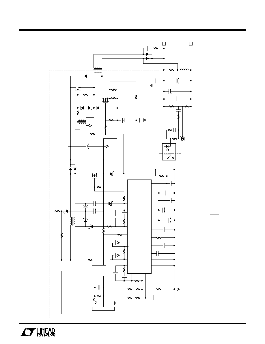
Typical Application
Figure 9 shows a 24VDC, 300W power factor corrected,
universal input supply. The 2-transistor forward converter
offers many benefits including low peak currents,
nondissipative snubber, 500VDC switches and automatic
core reset guaranteed by the LT1508's 50% maximum
duty cycle.
13
LT1508
Figure 9. 24V, 300W Off-Line PFC Supply
APPLICATIO
N
S I
N
FOR
M
ATIO
N
W
U
U
U
Danger!! Lethal Voltages Present
V
SENSE
OVP
I
AC
R27
20k
1%
R35
499k
1%
R22
330k
R24
10k
R1
0.15
5W
V
IN
R3
91k
1W
R33
499k
1%
R32
499k
1%
R34
499k
1%
382VBUS
14
11
9
V
CC
V
REF
V
C
17
18
6
5
4
1
2
3
I
LIM
GTDR2
LT1508
VA
OUT
V
REF
PK
LIM
GTDR1
M
OUT
I
SENSE
CA
OUT
C2
0.47
µ
F
C30
120
µ
F
35V
C26
120
µ
F
35V
R25
20k
R11
20
C24
1nF
C29
300pF
C6
2.2
µ
F
50V
C8
330
µ
F
35V
C7
2.2
µ
F
50V
D9
1N5818
D10
1N5818
Q1
IRFP450
D3
ERA82-004
D2
ERA82-004
D4
MURH860CT
V
OUT
382VBUS
D1
ERA82-004
T1
C3
0.1
µ
F
C23
47nF
C9
1
µ
F
"X"
R2
1M
1/2W
1
2
3
LINE
LINE
GND
12
10
1
3
2
4
58
7
6
1
V
IN
V
REF
R36
4.02k
1%
RT1
SG57
R16
15k
1%
R26
20k
1%
NOTE: UNLESS OTHERWISE SPECIFIED
1. ALL RESISTORS 1/4W, 5%
2. ALL CAPACITANCE VALUES IN MICROFARADS
T1: COILTRONICS CTX02-13141-X2 (407) 241-7876
T2: COILTRONICS CTX02-13063-X3
T3: BI TECHNOLOGY HM41-11510 (714) 447-2345
F1
6.3F
E1
90VAC TO
264VAC
19
20
Danger!! Lethal Voltages Present
In This Section
C25
1nF
C21
1nF
C22
4.7nF
C20
47nF
C32
1
µ
F
C31
1
µ
F
C19
10nF
C11
1
µ
F
63V
E3
COM
C4
4.7nF
"Y"
C18
0.1
µ
F
0.068
µ
F
C33
1
µ
F
R37
4.02k
1%
R39
20k
R14
3.3
15V
GND2
GND1
C
SET
SS2
R
SET
SS1
23
4
1
3
1
5
1
6
15V
+
+
R21
2K
U4
LT1431
1508 F09
U3
CNY17-3
R20
2.2k
R19
1k
33
R31
30.1k
1%
R6
10
2W
D11
MUR3020PT
R7
10
1W
R30
3.4k
1%
C12
1000
µ
F
35V
+
C13
1000
µ
F
35V
L1
67
µ
F
+
E2
24V
C16
1nF
R9
10
D8
MUR160
D5
1N965B
15V
D6
1N965B
15V
R41
20k
C28
100pF
R40
470
R8
10
+
~
~
U1
KPBC606
+
+
+
+
D7
MUR160
Q1
IRF840
T2
Q3
IRF840
C1
1
µ
F
400V
C14
330
µ
F
450V
C10
1
µ
F
63V
T3
R5
0.51
R4
0.51
R13
20k
R10
20
C5
4.7nF
"Y"
C1: ELECTRONIC CONCEPTS 5MP12J105K
L1: COILTRONICS CTX02-13140-X3
R
1: JW MILLER/FUKUSHIMA MPC71
RT1: KETEMA SG57 SURGE GARD
·
·
·
·
·
·

14
LT1508
APPLICATIO
N
S I
N
FOR
M
ATIO
N
W
U
U
U
An LT1431 reference/amplifier coupled to a low cost
optoisolator closes the loop from secondary side to pri-
mary side. Efficiency versus power and line voltage is
shown in Figure 10. The PFC preregulator alone has
efficiency numbers between 90% and 97% over line and
load.
A 3-turn secondary added to the 70-turn primary of T1
bootstraps V
CC
to about 15V supplying the chip's 13mA
requirement as well as about 39mA to cover the gate
current of the three FETs and high side transformer. A
0.15
sense resistor is used to sense input current and
servo to the command created by the outer voltage and
multiplier. Thus the input current follows the input line
voltage, and changes as necessary, in order to maintain
constant bank voltage. The forward converter sees a
voltage input of 382VDC unless the line voltage drops out,
in which case the 330
µ
F main capacitor discharges to
240VDC before the PWM stage is shut down. Compared to
a typical off-line converter, the effective input voltage
range of the forward converter is much smaller, simplify-
ing the design. Additionally, the higher bus voltage pro-
vides greater hold-up times for given capacitor size.
V
RMS
90
EFFICIENCY (%)
80
85
250
1508 · F1O
75
70
132
180
90
200W/300W
100W
30W
Figure 10

15
LT1508
Dimensions in inches (millimeters) unless otherwise noted.
PACKAGE DESCRIPTIO
N
U
Information furnished by Linear Technology Corporation is believed to be accurate and reliable.
However, no responsibility is assumed for its use. Linear Technology Corporation makes no represen-
tation that the interconnection of its circuits as described herein will not infringe on existing patent rights.
N Package
20-Lead PDIP (Narrow 0.300)
(LTC DWG # 05-08-1510)
N20 0695
0.015
(0.381)
MIN
0.125
(3.175)
MIN
0.130
±
0.005
(3.302
±
0.127)
0.065
(1.651)
TYP
0.045 0.065
(1.143 1.651)
0.018
±
0.003
(0.457
±
0.076)
0.005
(0.127)
MIN
0.100
±
0.010
(2.540
±
0.254)
0.255
±
0.015*
(6.477
±
0.381)
1.040*
(26.416)
MAX
1
2
3
4
5
6
7
8
9
10
19
11
12
13
14
16
15
17
18
20
0.009 0.015
(0.229 0.381)
0.300 0.325
(7.620 8.255)
0.325
+0.025
0.015
+0.635
0.381
8.255
(
)
*THESE DIMENSIONS DO NOT INCLUDE MOLD FLASH OR PROTRUSIONS.
MOLD FLASH OR PROTRUSIONS SHALL NOT EXCEED 0.010 INCH (0.254mm)

16
LT1508
©
LINEAR TECHNOLOGY CORPORATION 1995
1508f LT/TP 0697 7K · PRINTED IN USA
Dimensions in inches (millimeters) unless otherwise noted.
PACKAGE DESCRIPTIO
N
U
SW Package
20-Lead Plastic Small Outline (Wide 0.300)
(LTC DWG # 05-08-1620)
S20 (WIDE) 0396
NOTE 1
0.496 0.512*
(12.598 13.005)
20
19
18
17
16
15
14
13
1
2
3
4
5
6
7
8
0.394 0.419
(10.007 10.643)
9
10
11
12
0.037 0.045
(0.940 1.143)
0.004 0.012
(0.102 0.305)
0.093 0.104
(2.362 2.642)
0.050
(1.270)
TYP
0.014 0.019
(0.356 0.482)
TYP
0
°
8
°
TYP
NOTE 1
0.009 0.013
(0.229 0.330)
0.016 0.050
(0.406 1.270)
0.291 0.299**
(7.391 7.595)
×
45
°
0.010 0.029
(0.254 0.737)
NOTE:
1. PIN 1 IDENT, NOTCH ON TOP AND CAVITIES ON THE BOTTOM OF PACKAGES ARE THE MANUFACTURING OPTIONS.
THE PART MAY BE SUPPLIED WITH OR WITHOUT ANY OF THE OPTIONS
DIMENSION DOES NOT INCLUDE MOLD FLASH. MOLD FLASH SHALL NOT EXCEED 0.006" (0.152mm) PER SIDE
DIMENSION DOES NOT INCLUDE INTERLEAD FLASH. INTERLEAD FLASH SHALL NOT EXCEED 0.010" (0.254mm) PER SIDE
*
**
PART NUMBER
DESCRIPTION
COMMENTS
LT1084
5A Low Dropout Linear Regulator
Good for Post Regulation of Switching Power Supplies
LT1105
Simplified Off-Line Controller
Solution for Universal Off-Line Inputs with Output to 100W
LT1241-5
High Frequency Current Mode PWM Controller
Operates at Oscillator Frequencies up to 500kHz
LT1247
High Frequency Current Mode PWM Controller
Operates at Oscillator Frequencies up to 1MHz
LT1248
Full-Feature Average Current Mode Power Factor Controller
Provides All Features in 16-Lead Package
LT1249
Minimal Parts Count Power Factor Controller
Simplified PFC Design
LT1509
Power Factor and PWM Controller
Current Mode PWM
RELATED PARTS
Linear Technology Corporation
1630 McCarthy Blvd., Milpitas, CA 95035-7417
q
(408) 432-1900
FAX: (408) 434-0507
q
TELEX: 499-3977
q
www.linear-tech.com