
1
LT1024
1024fa
Guaranteed Offset Voltage: 50ÁV Max
Guaranteed Bias Current:
25░C: 120pA Max
ş 55░C to 125░C: 700pA Max
Guaranteed Drift: 1.5ÁV/░C Max
Low Noise, 0.1Hz to 10Hz: 0.5ÁV
P-P
Guaranteed Supply Current: 600ÁA Max
Guaranteed CMRR: 112dB Min
Guaranteed PSRR: 112dB Min
Guaranteed Voltage Gain with 5mA Load Current
Guaranteed Matching Characteristics
The LT
«
1024 dual, matched internally compensated
universal precision operational amplifier can be used in
practically all precision applications requiring multiple op
amps. The LT1024 combines picoampere bias currents
(which are maintained over the full ş55░C to 125░C
temperature range), microvolt offset voltage (and low drift
with time and temperature), low voltage and current
noise and low power dissipation. Extremely high
common mode and power supply rejection ratios,
practically immeasurable warm-up drift, and the ability to
deliver 5mA load current with a voltage gain of a million,
round out the LT1024's superb precision specifications.
Tight matching is guaranteed on offset voltage,
noninverting bias currents and common mode and power
supply rejections.
The all-around excellence of the LT1024 eliminates the
necessity of the time-consuming error analysis procedure
of precision system design in many dual applications; the
LT1024 can be stocked as the universal dual op amp in the
14-pin DIP configuration.
For a single op amp with similar specifications, see the
LT1012 data sheet; for a single supply dual precision op
amp in the 8-pin configuration, see the LT1013 data sheet.
Strain Gauge Signal Conditioner
Dual Limit Precision Threshold Detection
Charge Integrators
Wide Dynamic Range Logarithmic Amplifiers
Light Meters
Low Frequency Active Filters
Standard Cell Buffers
Thermocouple Amplifiers
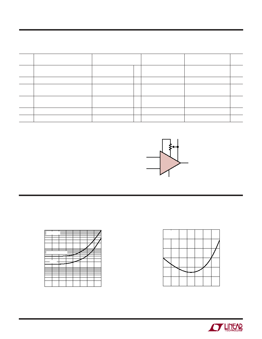
Two Op Amp Instrumentation Amplifier
Dual, Matched
Picoampere, Microvolt Input,
Low Noise Op Amp
Input Bias Current vs Temperature
TEMPERATURE (░C)
ş50
ş150
INPUT BIAS CURRENT (pA)
ş50
100
0
50
75
LTC1024 Ě TA02
ş100
50
0
ş25
25
100
125
UNDERCANCELLED UNIT
OVERCANCELLED UNIT
, LTC and LT are registered trademarks of Linear Technology Corporation.
LT1024 Ě TA01
6
OUTPUT
TYPICAL PERFORMANCE:
OFFSET VOLTAGE = 20
Á
V
BIAS CURRENT =
▒
30pA
OFFSET CURRENT = 30pA
4
3
13
1/2 LT1024
+
ş
(
)
ş
+
1/2 LT1024
+
ş
INPUTS
R1*
100k
R3
10k
R2
10k
R5
2.2k
R4
100k
10
11
GAIN =
~ 100
1 + 1
2
R2
R1
R3
R4
R4
R3
R2 + R3
R5
+
+
~
TRIM FOR COMMON-MODE REJECTION
TRIM FOR GAIN
*
APPLICATIO S
U
FEATURES
DESCRIPTIO
U
TYPICAL APPLICATIO
U

2
L T1 0 2 4
1024fa
ORDER
PART NUMBER
LT1024ACN
LT1024CN
NOTE: DEVICE MAY BE OPERATED EVEN IF
INSERTION IS REVERSED; THIS IS DUE
TO INHERENT SYMMETRY OF PIN LOCATIONS
OF AMPLIFIERS A AND B (NOTE 3)
D PACKAGE
14-PIN SIDE BRAZED (HERMETIC)
T
JMAX
= 150
░
C,
JA
= 100
░
C/W,
JC
= 60
░
C/W (D)
N PACKAGE
14-PIN PDIP
T
JMAX
= 100
░
C,
JA
= 100
░
C/W,
JC
= 60
░
C/W (N)
1
2
3
4
5
6
7
TOP VIEW
14
13
12
11
10
9
8
NULL (A)
NULL (A)
şIN (A)
+IN (A)
V
ş
(B)
OUT (B)
V
+
(B)
V
+
(A)
OUT (A)
V
ş
(A)
+IN (B)
şIN (B)
NULL (B)
NULL (B)
ş
ş
+
+
A
B
ORDER
PART NUMBER
LT1024AMD
LT1024MD
Supply Voltage ...................................................... ▒20V
Differential Input Current (Note 2) ...................... ▒10mA
Input Voltage ......................................................... ▒20V
Output Short Circuit Duration .......................... Indefinite
Operating Temperature Range
LT1024AM/LT1024M (OBSOLETE).....ş 55░C to 125░C
LT1024AC/LT1024C ................................ 0░C to 70░C
Storage Temperature Range ................. ş 65░C to 150░C
Lead Temperature (Soldering, 10 sec).................. 300░C
(Note 1)
Consult LTC Marketing for parts specified with wider operating temperature ranges.
OBSOLETE PACKAGE
Consider the N14 Package as an Alternate Source
LT1O24AM/LT1O24AC
LT1024M/LT1O24C
SYMBOL
PARAMETER
CONDITIONS
MIN
TYP
MAX
MIN
TYP
MAX
UNITS
V
OS
Input Offset Voltage
15
50
20
100
ÁV
Long Term Input Offset Voltage Stability
0.3
0.3
ÁV/month
I
OS
Input Offset Current
20
100
25
180
pA
I
B
Input Bias Current
▒25
▒120
▒30
▒200
pA
e
n
Input Noise Voltage
0.1Hz to 10Hz
0.5
0.5
ÁV
P-P
e
n
Input Noise Voltage Density
f
O
= 10Hz (Note 4)
17
33
17
33
nV/Hz
f
O
= 1000Hz (Note 4)
14
24
14
24
nV/Hz
i
n
Input Noise Current Density
f
O
= 10Hz
20
20
fA/Hz
A
VOL
Large-Signal Voltage Gain
V
OUT
= ▒12V, R
L
10k
250
2000
180
2000
V/mV
V
OUT
= ▒10V, R
L
2k
150
1000
100
1000
V/mV
CMRR
Common Mode Rejection Ratio
V
CM
= ▒13.5V
112
132
108
132
dB
PSRR
Power Supply Rejection Ratio
V
S
= ▒2V to ▒20V
112
132
108
132
dB
Input Voltage Range
▒13.5
▒14.0
▒13.5
▒14.0
V
V
OUT
Output Voltage Swing
R
L
= 10k
▒13
▒14
▒13
▒14
V
Slew Rate
0.1
0.2
0.1
0.2
V/Ás
I
S
Supply Current per Amplifier
380
600
380
700
ÁA
Individual Amplifiers. V
S
= ▒15V, V
CM
= 0V, T
A
= 25░C unless otherwise noted.
ABSOLUTE AXI U RATI GS
W
W
W
U
PACKAGE/ORDER I FOR ATIO
U
U
W
ELECTRICAL CHARACTERISTICS

3
LT1024
1024fa
LT1024AM/LT1024AC
LT1O24M /LT1O24C
SYMBOL
PARAMETER
CONDITIONS
MIN
TYP
MAX
MIN
TYP
MAX
UNITS
Input Offset Voltage Match
20
75
25
150
ÁV
I
B
+
Average Noninverting Bias
▒30
▒150
▒40
▒250
pA
Current
I
OS
+
Noninverting Offset Current
30
150
30
300
pA
CMRR
Common Mode Rejection Ratio
V
CM
= ▒13.5V
110
132
106
132
dB
Match
PSRR
Power Supply Rejection Ratio
V
S
= ▒2V to 20V
110
132
106
132
dB
Match
Channel Separation
f 10Hz (Note 4)
134
150
134
150
dB
LT1024AM/LT1024AC
LT1024M/LT1024C
SYMBOL
PARAMETER
CONDITIONS
MIN
TYP
MAX
MIN
TYP
MAX
UNITS
V
OS
Input Offset Voltage
0░C to 70░C
30
120
35
200
ÁV
ş55░C to 125░C
40
200
50
300
ÁV
Average Temperature Coefficient of
0.25
1.5
0.3
2.0
ÁV/░C
Input Offset Voltage
I
OS
Input Offset Current
0░C to 70░C
40
250
50
300
pA
ş 55░C to 125░C
80
350
100
500
pA
Average Temperature Coefficient of
0.5
2.5
0.7
3
pA/░C
Input Offset Current
I
B
Input Bias Current
0░C to 70░C
▒40
▒250
▒50
▒400
pA
ş 55░C to 125░C
▒100
▒700
▒200
▒1300
pA
Average Temperature Coefficient of
0░C to 70░C
0.4
3
0.5
4
pA/░C
Input Bias Current
ş 55░C to 125░C
1
6
2
12
pA/░C
A
VOL
Large-Signal Voltage Gain
V
OUT
= ▒12V, R
L
10k
150
1000
150
1000
V/mV
V
OUT
= ▒10V, R
L
2k
100
600
100
600
V/mV
CMRR
Common Mode Rejection Ratio
V
CM
= ▒13.5V
108
128
106
128
dB
PSRR
Power Supply Rejection Ratio
V
S
= ▒2.5V to ▒18V
108
128
106
128
dB
Input Voltage Range
▒13.5
▒13.5
V
V
OUT
Output Voltage Swing
R
L
= 10k
▒13
▒14
▒13
▒14
V
I
S
Supply Current
400
800
400
900
ÁA
Matching Specifications. V
S
= ▒15V, V
CM
= 0V, T
A
= 25░C unless otherwise noted.
Individual Amplifiers. The
denotes the specifications which apply over the full operating temperature range of 0░C T
A
= 70░C for
the LT1024AC and LT1024C; ş 55░C T
A
125░C for the LT1024AM and LT1024M. V
S
= ▒15V, V
CM
= 0V, unless otherwise noted.
ELECTRICAL CHARACTERISTICS
4
L T1 0 2 4
1024fa
LT1024AM/LT1024AC
LT1024M/LT1024C
SYMBOL
PARAMETER
CONDITIONS
MIN
TYP
MAX
MIN
TYP
MAX
UNITS
Input Offset Voltage Match
0░C to 70░C
35
170
45
300
ÁV
ş 55░C to 125░C
50
280
70
500
ÁV
Input Offset Voltage Tracking
0.3
2
0.4
3.5
ÁV/░C
I
B
+
Average Noninverting Bias Current
0░C to 70░C
▒40
▒300
▒50
▒500
pA
ş 55░C to 125░C
▒100
▒800
▒200
▒1400
pA
I
OS
+
Noninverting Offset Current
0░C to 70░C
40
300
50
500
pA
ş 55░C to 125░C
80
800
150
1500
pA
CMRR
Common Mode Rejection Ratio Match V
CM
= ▒13.5V
106
128
104
128
dB
PSRR
Power Supply Rejection Ratio Match
V
S
= ▒2.5V to ▒18V
106
128
104
128
dB
Note 1: Absolute Maximum Ratings are those values beyond which the life
of a device may be impaired.
Note 2: Differential input voltages greater than 1V will cause excessive
current to flow through the input protection diodes unless limiting
resistance is used.
Note 3: The V
+
supply terminals are completely independent and may be
powered by separate supplies if desired (this approach, however, would
sacrifice the advantages of the power supply rejection ratio matching). The
V
ş
supply terminals are both connected to the common substrate and
must be tied to the same voltage. Both V
ş
pins should be used.
Note 4: This parameter is tested on a sample basis only.
Optional Offset Nulling Circuit
Offset Voltage vs Source
Resistance (Balanced or Unbalanced)
Input Offset Current vs
Temperature
14 (7)
5k TO 100k
POT
2 (9)
1 (8)
13
(6)
OUTPUT
INPUT OFFSET VOLTAGE CAN BE ADJUSTED
OVER A ▒800ÁV RANGE WITH A 5k TO
100k POTENTIOMETER
1/2
LT1024
+
ş
3
4
(10)
(11)
12 (5)
Vş
V+
LT1024 Ě EC01
SOURCE RESISTANCE (
)
1k
1
INPUT OFFSET VOLTAGE (
Á
V) 100
1000
100k
10k
300k 1M
3M 10M
30k
3k
10
LT1024 Ě TPC01
25
░
C
ş 55
░
C TO 125
░
C
V
S
=
▒
15V
ş 50
INPUT OFFSET CURRENT (pA)
40
50
60
25
75
30
20
ş25
0
50
100
125
10
0
TEMPERATURE (░C)
LT1024 Ě TPC02
V
S
= ▒15V
V
CM
= 0V
Matching Specifications. The
denotes the specifications which apply over
the temperature range of 0░C T
A
= 70░C for the LT1024AC and LT1024C; ş 55░C T
A
125░C for the LT1024AM and LT1024M,
V
S
= ▒15V, V
CM
= 0V unless otherwise noted.
ELECTRICAL CHARACTERISTICS
TYPICAL PERFOR A CE CHARACTERISTICS
U
W

5
LT1024
1024fa
FREQUENCY (Hz)
1
140
120
100
80
60
40
20
0
1k
100k
10
100
10k
1M
COMMON MODE REJECTION RATIO (dB)
V
S
=
▒
15V
T
A
= 25
░
C
LT1024 Ě TPC10
CMRR
MATCH
(
CMRR)
TIME (SECONDS)
0
NOISE VOLTAGE 400nV/DIVISION
8
2
4
6
10
T
A
= 25░C
V
S
▒2V TO ▒ 20V
LT1024 Ě TPC07
Offset Voltage Drift and
Tracking with Temperatures of
Representative Units
0
CHANGE IN OFFSET VOLTAGE (
Á
V)
3
4
5
4
2
1
0
1
2
3
5
TIME AFTER POWER ON (MINUTES)
V
S
= ▒15V
T
A
= 25░C
LT1024 Ě TPC04
Warm-Up Drift
Input Bias Current Over
Common Mode Range
Supply Current vs Supply
Voltage per Amplifier
0.1Hz to 10Hz Noise
Noise Spectrum
Total Noise vs Source
Resistance
Common Mode Rejection and
CMRR Match vs Frequency
COMMON MODE INPUT VOLTAGE (V)
ş15
ş 60
INPUT BIAS CURRENT (pA)
ş40
ş20
0
20
60
ş10
ş 5
0
5
10
15
40
V
S
=
▒
15V
T
A
= 25
░
C
DEVICE WITH POSITIVE
INPUT CURRENT
DEVICE WITH NEGATIVE
INPUT CURRENT
R
IN CM
= 2 x 10
12
LT1024 Ě TPC03
I
B
V
CM
ş
+
ş 50
OFFSET VOLTAGE (
Á
V)
20
40
60
25
75
0
ş20
ş25
0
50
100
125
ş 40
ş 60
TEMPERATURE (░C)
LT1024 Ě TPC05
INDIVIDUAL AMPLIFIERS
TRACKING (MATCH DRIFT)
V
S
= ▒15V
2
1
1
2
2
2
1
SUPPLY VOLTAGE (V)
0
SUPPLY CURRENT (
Á
A)
400
▒ 20
25░C
125░C
ş55░C
300
▒ 5
▒10
▒15
500
LT1024 Ě TPC06
Power Supply Rejection vs
Frequency
FREQUENCY (Hz)
0.1
POWER SUPPLY REJECTION RATIO (dB)
100
120
140
100
10k
80
60
1
10
1k
100k
1M
40
20
V
S
= ▒15V
T
A
= 25░C
NEGATIVE
SUPPLY
POSITIVE
SUPPLY
LT1024 Ě TPC11
TOTAL NOISE DENSITY (
Á
V/
Hz)
SOURCE RESISTANCE (
)
10
2
10
3
10
4
10
5
10
6
10
7
0.01
1.0
10.0
10
8
0.1
T
A
= 25
░
C
V
S
=
▒
2V TO
▒
20V
AT 10Hz
AT 1kHz
RESISTOR NOISE
ONLY
AT 10Hz
LT1024 Ě TPC09
R
R
R
S
= 2R
+
ş
AT 1kHz
FREQUENCY (Hz)
1
1
CURRENT NOISE DENSITY (fA/
Hz)
10
100
1000
10
100
1000
VOLTAGE NOISE DENSITY (nV/
Hz)
T
A
= 25░C
V
S
▒2 TO ▒20V
1/f CORNER
2.5Hz
CURRENT NOISE
VOLTAGE NOISE
LT1024 Ě TPC08
1/f CORNER
120Hz
TYPICAL PERFOR A CE CHARACTERISTICS
U
W
6
L T1 0 2 4
1024fa
Gain, Phase Shift vs Frequency
Voltage Gain vs Frequency
Channel Separation vs
Frequency
Voltage Gain vs Load Resistance
Small-Signal Transient
Response
Small-Signal Transient
Response
Large-Signal Transient
Response
FREQUENCY (Hz)
100
CHANNEL SEPARATION (dB)
120
130
150
160
100
1M
LT1024 Ě TPC12
80
1k
100k
10k
140
110
90
V
S
=
▒
15V
T
A
= 25
░
C
R
S
= 10
R
S
= 100
R
S
= 1k
FREQUENCY (Hz)
0.01
VOLTAGE GAIN (dB)
60
80
100
100 1k 10k 100k 1M 10M
40
20
ş20
0.1
1
10
0
140
120
LT1024 Ě TPC13
V
S
= ▒15V
T
A
= 25░C
FREQUENCY (MHz)
0.01
ş10
GAIN (dB)
PHASE SHIFT (DEGREES)
20
30
40
0.1
1
10
10
0
200
140
120
100
160
180
GAIN
LT1024 Ě TPC14
PHASE MARGIN
= 70
░C
T
A
= 25░C
V
S
= ▒15V
PHASE
LOAD RESISTANCE (k
)
1
100k
300k
1M
10M
3M
VOLTAGE GAIN
5
2
10
20
V
S
=
▒
15V
V
0
=
▒
10V
25
░
C
125
░
C
ş 55
░
C
LT1024 Ě TPC15
20mV/DIVISION
5Ás/DIV
20mV/DIVISION
5Ás/DIV
2V/DIVISION
20Ás/DIV
A
V
= +1
C
LOAD
= 100pF
A
V
= +1
C
LOAD
= 1000pF
A
V
= +1
TYPICAL PERFOR A CE CHARACTERISTICS
U
W

7
LT1024
1024fa
The LT1024 may be inserted directly into OP-10, OP-207
or 0P227 sockets with or without removal of external
nulling components.
The LT1024 is specified over a wide range of power supply
voltages from ▒2V to ▒18V. Operation with lower supplies
is possible down to ▒1.2V (two NiCad batteries).
Advantages of Matched Dual Op Amps
In many applications, the performance of a system
depends on the matching between two operational
amplifiers rather than the individual characteristics of the
two op amps. Two or three op amp instrumentation
amplifiers, tracking voltage references, and low drift active
filters are some of the circuits requiring matching between
two op amps.
The well-known triple op amp configuration illustrates
these concepts. Output offset is a function of the dif-
ference between the offsets of the two halves of the
LT1024. This error cancellation principle holds for a
considerable number of input-referred parameters in
addition to offset voltage and its drift with temperature.
Input bias current will be the average of the two
noninverting input currents (I
B
+
). The difference between
these two currents (I
OS
+
) is the offset current of the
instrumentation amplifier. Common mode and power
supply rejections will be dependent only on the match
between the two amplifiers (assuming perfect resistor
matching).
The concepts of common mode and power supply rejec-
tion ratio match (CMRR and PSRR) are best demon-
strated with a numerical example:
Assume CMRR
A
= +1.0ÁV/V or 120dB
and CMRR
B
= + 0.5ÁV/V or 126dB,
then CMRR = 0.5ÁV/V or 126dB
if CMRR
B
= ş 0.5ÁV/V, which is still 126dB,
then CMRR = 1.5ÁV/V or 116.5dB.
Typical performance of the instrumentation amplifier:
Input offset voltage = 25ÁV.
Input bias current = 30pA.
Input resistance = 10
12
.
Input offset current = 30pA.
Input noise = 0.7ÁV
P-P
.
Power bandwidth (V
O
= ▒10V) = 80kHz.
Clearly, the LT1024, by specifying and guaranteeing all of
these matching parameters, can significantly improve the
performance of matching dependent circuits.
Three Op Amp Instrumentation Amplifier
LT1024 Ě AI01
TRIM R8 FOR GAIN
TRIM R9 FOR DC COMMON MODE REJECTION
TRIM R10 FOR AC COMMON MODE REJECTION
3
2
3
4
11
10
5
6
7
4
6
7
12
OUTPUT
13
14
R4
100
1%
R6
10k
1%
R5
100
1%
R1
10k
1%
R3
2.1k
1%
R7
9.76k
1%
R2
10k
1%
R10
100k
R9
500
R8
200
C1
100pF
LT1037
A
1/2 LT1024
B
1/2 LT1024
şINPUT
+INPUT
15V
15V
ş15V
ş15V
15V
ş15V
GAIN = 1000
ş
+
ş
+
ş
+
APPLICATIO S I FOR ATIO
W
U
U
U

8
L T1 0 2 4
1024fa
Achieving Picoampere/Microvolt Performance
In order to realize the picoampere/microvolt level
accuracy of the LT1024, proper care must be exercised.
For example, leakage currents in circuitry external to the
op amp can significantly degrade performance. High qual-
ity insulation should be used (e.g., TeflonTM, Kel-F); clean-
ing of all insulating surfaces to remove fluxes and other
residues will probably be required. Surface coating may be
necessary to provide a moisture barrier in high humidity
environments.
Board leakage can be minimized by encircling the input
circuitry with a guard ring operated at a potential close to
that of the inputs: in inverting configurations, the guard
ring should be tied to ground; in noninverting connec-
tions, to the inverting input. Guarding both sides of the
printed circuit board is required. Bulk leakage reduction
depends on the guard ring width. Nanoampere level leak-
age into the offset trim terminals can affect offset voltage
and drift with temperature.
Microvolt level error voltages can also be generated in the
external circuitry. Thermocouple effects, caused by tem-
perature gradients across dissimilar metals at the con-
tacts to the input terminals, can exceed the inherent drift
of the amplifier. Air currents over device leads should be
minimized, package leads should be short, and the two
input leads should be as close together as possible and
maintained at the same temperature.
Test Circuit for Offset Voltage and its Drift with Temperature
R1
50k*
R3
50k*
R2
100*
V
0
15V
ş15V
ş
+
3
(10)
4
(11)
LT1024
(7)
14
12 (5)
13
(6)
RESISTORS MUST HAVE LOW
THERMOELECTRIC POTENTIAL
THIS CIRCUIT IS ALSO USED AS THE BURN-IN
CONFIGURATION FOR THE LT1024. WITH SUPPLY
VOLTAGES INCREASED TO ▒20V, R1 = R3 = 20k,
R2 = 200, AV = 100
V
O
= 1000V
0S
LT1024 Ě AI02
*
**
Teflon is a trademark of Dupont.
APPLICATIO S I FOR ATIO
W
U
U
U
9
LT1024
1024fa
Direct Pressure Transducer to Digital Output Signal Conditioner
LT1024 Ě AI03
330
11
10
5
6
7
LT1024
15V
226k*
120k*
50k
GAIN TRIM
0.01ÁF
0.0047ÁF
OUT B
OUT A
ş15V
+
ş
+
ş
LT1024
ş15V
ş5V
ş5V
ş15V
15V
15V
TRANSDUCER
ZERO
1% METAL FILM RESISTOR
GATES = 74C00
TRANSDUCER = BLH # DHF-100 PSI
PRESSURE TRANSDUCER
0 ş 100 PSI = 0 ş 1000
COUNTS FULL-SCALE AT CIRCUIT OUTPUT
*
**
ş5V
ş15V
15V
10k
10ÁF
10k*
10k
10k
100k
100k
ADJ
LT137A OUT
V
IN
OUTPUT = f
OUT
A/f
OUT
B
f
CLK
~ 10kHz
2k
620
2N2979
1N4148
2N3904
4
3
12
14
13
2N3904
10k
28k
14k
10k
CLK
Q
PRE
CLR
74C74
Q
D
~
+
APPLICATIO S I FOR ATIO
W
U
U
U

10
L T1 0 2 4
1024fa
(11)
+INPUT
(10)
şINPUT
(5)
V
ş
320
330
40
4.3k
4.8k
3.3k
3.3k
16k
20k
3.3k
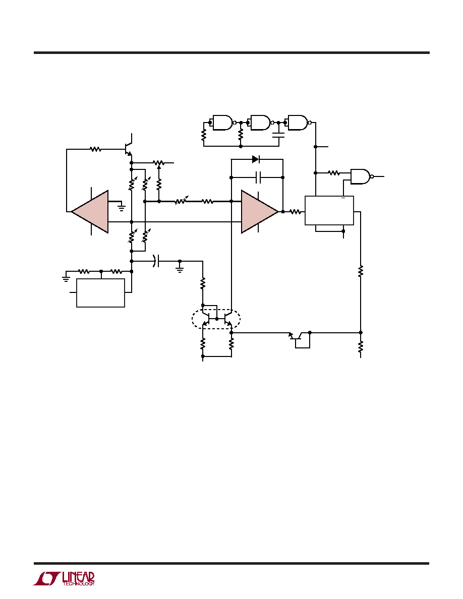
Q19
Q18
Q39
Q34
Q35
Q36
Q33
Q32
Q31
Q12
Q11
50k
1.5k
Q23
Q40
Q41
Q42
Q38
Q37
Q43
V
+
(7)
Q26
Q28
1.5k
40
100
40
OUTPUT
(6)
Q30
Q27
Q25
1.5k
Q15
Q2
Q13
Q16
Q5
Q7
22k
22k
800
800
1.3k
4.2k
Q8
Q14
4k
30pF
Q22
Q24
Q4
Q3
Q21
Q20
Q29
Q6
Q1
Q9
Q10
s
s
s
TRIM
(8)
3k
s
J1
Q17
LT1024 * SD01
14
13
12
4
3
1
TRIM
(9)
2
1/2
LT1024
SCHE ATIC DIAGRA
W
W
11
LT1024
1024fa
Information furnished by Linear Technology Corporation is believed to be accurate and reliable.
However, no responsibility is assumed for its use. Linear Technology Corporation makes no represen-
tation that the interconnection of its circuits as described herein will not infringe on existing patent rights.
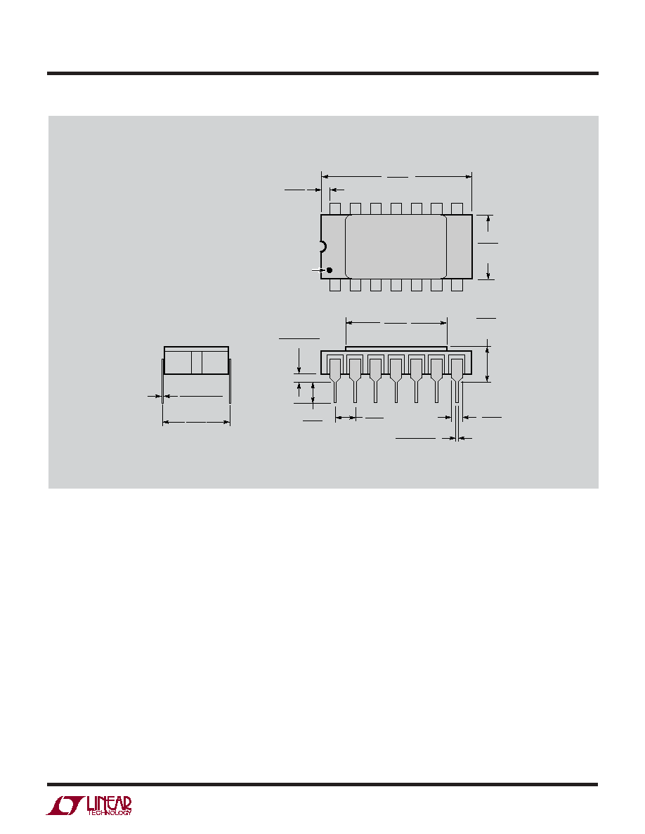
D Package
14-Lead Side Brazed (Hermetic)
(Reference LTC DWG # 05-08-1210)
OBSOLETE PACKAGE
D14 0801
.008 ş .015
(0.203 ş 0.381)
.300
(7.620)
REF
1
8
2
7
3
6
4
5
.290
(7.366)
TYP
.760
(19.304)
MAX
.005
(0.127)
MIN
9
10
11
12
13
14
PIN NO. 1
IDENT
.485
(12.319)
MAX
.125
(3.175)
MIN
.020 ş .060
(0.508 ş 1.524)
.100
(2.54)
BSC
.165
(4.191)
MAX
.015 ş .023
(0.381 ş 0.584)
.054
(1.372)
TYP
U
PACKAGE DESCRIPTIO
12
L T1 0 2 4
1024fa
Linear Technology Corporation
1630 McCarthy Blvd., Milpitas, CA 95035-7417
(408) 432-1900
FAX: (408) 434-0507
www.linear.com
LW/TP 1002 1K REV A Ě PRINTED IN USA
LINEAR TECHNOLOGY CORPORATION 1988
PART NUMBER
DESCRIPTION
COMMENTS
LT1884
Picoamp Input, Precision Op Amp
Rail-to-Rail Output
N14 1002
.020
(0.508)
MIN
.120
(3.048)
MIN
.130 ▒ .005
(3.302 ▒ 0.127)
.045 ş .065
(1.143 ş 1.651)
.065
(1.651)
TYP
.018 ▒ .003
(0.457 ▒ 0.076)
.005
(0.125)
MIN
.255 ▒ .015*
(6.477 ▒ 0.381)
.770*
(19.558)
MAX
3
1
2
4
5
6
7
8
9
10
11
12
13
14
.008 ş .015
(0.203 ş 0.381)
.300 ş .325
(7.620 ş 8.255)
.325
+.035
ş.015
+0.889
ş0.381
8.255
(
)
NOTE:
1. DIMENSIONS ARE
INCHES
MILLIMETERS
*THESE DIMENSIONS DO NOT INCLUDE MOLD FLASH OR PROTRUSIONS.
MOLD FLASH OR PROTRUSIONS SHALL NOT EXCEED .010 INCH (0.254mm)
.100
(2.54)
BSC
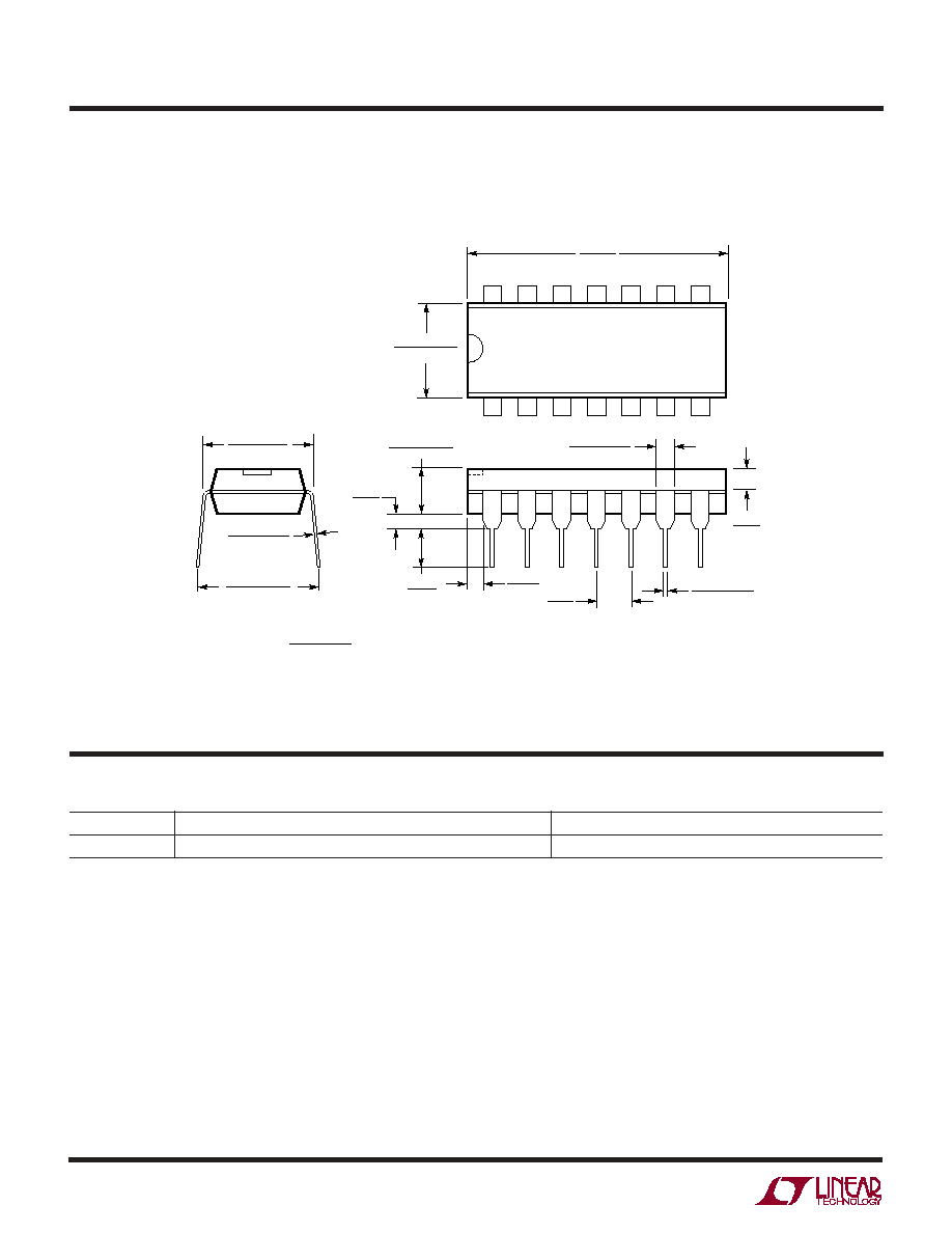
N Package
14-Lead PDIP (Narrow .300 Inch)
(Reference LTC DWG # 05-08-1510)
U
PACKAGE DESCRIPTIO
RELATED PARTS