N42S16400
IS42S16100A2
ISSI
®
Integrated Silicon Solution, Inc. -- www.issi.com --
1-800-379-4774
1
Rev. A
04/16/03
Copyright © 2003 Integrated Silicon Solution, Inc. All rights reserved. ISSI reserves the right to make changes to this specification and its products at any time
without notice. ISSI assumes no liability arising out of the application or use of any information, products or services described herein. Customers are advised to
obtain the latest version of this device specification before relying on any published information and before placing orders for products.
APRIL 2003
FEATURES
· Clock frequencies:
100 MHz, 143 MHz
· Fully synchronous; all signals referenced to a
positive clock edge
· Two banks can be operated simultaneously and
independently
· Dual internal bank controlled by A11 (bank select)
· Single 3.3V power supply
· LVTTL interface
· Programmable burst length
(1, 2, 4, 8, full page)
· Programmable burst sequence:
Sequential/Interleave
· Auto refresh, self refresh
· 4096 refresh cycles every 64 ms
· Random column address every clock cycle
· Programmable
CAS
latency: 3 clocks
· Burst read/write and burst read/single write
operations capability
· Burst termination by burst stop and precharge
command
· Byte controlled by LDQM and UDQM
· Package 400-mil 50-pin TSOP-II
DESCRIPTION
ISSI
's 16Mb Synchronous DRAM IS42S16100A2 is
organized as a 524,288-word x 16-bit x 2-bank for
improved performance. The synchronous DRAMs
achieve high-speed data transfer using pipeline
architecture. All inputs and outputs signals refer to the
rising edge of the clock input.
512K Words x 16 Bits x 2 Banks (16-MBIT)
SYNCHRONOUS DYNAMIC RAM
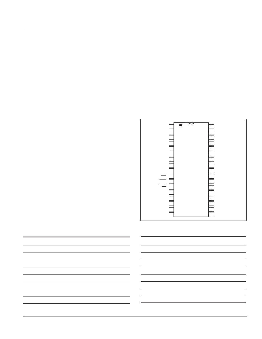
PIN CONFIGURATIONS
50-Pin TSOP (Type II)
PIN DESCRIPTIONS
A0-A11
Address Input
A0-A10
Row Address Input
A11
Bank Select Address
A0-A7
Column Address Input
DQ0 to DQ15
Data DQ
CLK
System Clock Input
CKE
Clock Enable
CS
Chip Select
RAS
Row Address Strobe Command
CAS
Column Address Strobe Command
WE
Write Enable
LDQM
Lower Bye, Input/Output Mask
UDQM
Upper Bye, Input/Output Mask
VDD
Power
GND
Ground
VDDQ
Power Supply for DQ Pin
GNDQ
Ground for DQ Pin
NC
No Connection
1
2
3
4
5
6
7
8
9
10
11
12
13
14
15
16
17
18
19
20
21
22
23
24
25
50
49
48
47
46
45
44
43
42
41
40
39
38
37
36
35
34
33
32
31
30
29
28
27
26
VDD
DQ0
DQ1
GNDQ
DQ2
DQ3
VDDQ
DQ4
DQ5
GNDQ
DQ6
DQ7
VDDQ
LDQM
WE
CAS
RAS
CS
A11
A10
A0
A1
A2
A3
VDD
GND
DQ15
IDQ14
GNDQ
DQ13
DQ12
VDDQ
DQ11
DQ10
GNDQ
DQ9
DQ8
VDDQ
NC
UDQM
CLK
CKE
NC
A9
A8
A7
A6
A5
A4
GND

IS42S16100A2
ISSI
®
2
Integrated Silicon Solution, Inc. -- www.issi.com --
1-800-379-4774
Rev. A
04/16/03
PIN FUNCTIONS
Pin No.
Symbol
Type
Function (In Detail)
20 to 24
A0-A10
Input Pin
A0 to A10 are address inputs. A0-A10 are used as row address inputs during active
27 to 32
command input and A0-A7 as column address inputs during read or write command
input. A10 is also used to determine the precharge mode during other commands. If
A10 is LOW during precharge command, the bank selected by A11 is precharged,
but if A10 is HIGH, both banks will be precharged.
When A10 is HIGH in read or write command cycle, the precharge starts
automatically after the burst access.
These signals become part of the OP CODE during mode register set command
input.
19
A11
Input Pin
A11 is the bank selection signal. When A11 is LOW, bank 0 is selected and when
high, bank 1 is selected. This signal becomes part of the OP CODE during mode
register set command input.
16
CAS
Input Pin
CAS
, in conjunction with the
RAS
and
WE
, forms the device command. See the
"Command Truth Table" item for details on device commands.
34
CKE
Input Pin
The CKE input determines whether the CLK input is enabled within the device. When
is CKE HIGH, the next rising edge of the CLK signal will be valid, and when LOW,
invalid. When CKE is LOW, the device will be in either the power-down mode, the
clock suspend mode, or the self refresh mode. The CKE is an asynchronous input.
35
CLK
Input Pin
CLK is the master clock input for this device. Except for CKE, all inputs to this device
are acquired in synchronization with the rising edge of this pin.
18
CS
Input Pin
The
CS
input determines whether command input is enabled within the device.
Command input is enabled when
CS
is LOW, and disabled with
CS
is HIGH. The
device remains in the previous state when
CS
is HIGH.
2, 3, 5, 6, 8, 9, 11
DQ0 to
DQ Pin
DQ0 to DQ15 are DQ pins. DQ through these pins can be controlled in byte units
12, 39, 40, 42, 43,
DQ15
using the LDQM and UDQM pins.
45, 46, 48, 49
14, 36
LDQM,
Input Pin
LDQM and UDQM control the lower and upper bytes of the DQ buffers. In read
UDQM
mode, LDQM and UDQM control the output buffer. When LDQM or UDQM is LOW,
the corresponding buffer byte is enabled, and when HIGH, disabled. The outputs go
to the HIGH impedance state when LDQM/UDQM is HIGH. This function
corresponds to
OE
in conventional DRAMs. In write mode, LDQM and UDQM control
the input buffer. When LDQM or UDQM is LOW, the corresponding buffer byte is
enabled, and data can be written to the device. When LDQM or UDQM is HIGH, input
data is masked and cannot be written to the device.
17
RAS
Input Pin
RAS
, in conjunction with
CAS
and
WE
, forms the device command. See the
"Command Truth Table" item for details on device commands.
15
WE
Input Pin
WE
, in conjunction with
RAS
and
CAS
, forms the device command. See the
"Command Truth Table" item for details on device commands.
7, 13, 38, 44
VDDQ
Power Supply Pin
VDDQ is the output buffer power supply.
1, 25
VDD
Power Supply Pin
VDD is the device internal power supply.
4, 10, 41, 47
GNDQ
Power Supply Pin
GNDQ is the output buffer ground.
26, 50
GND
Power Supply Pin
GND is the device internal ground.
IS42S16100A2
ISSI
®
Integrated Silicon Solution, Inc. -- www.issi.com --
1-800-379-4774
3
Rev. A
04/16/03
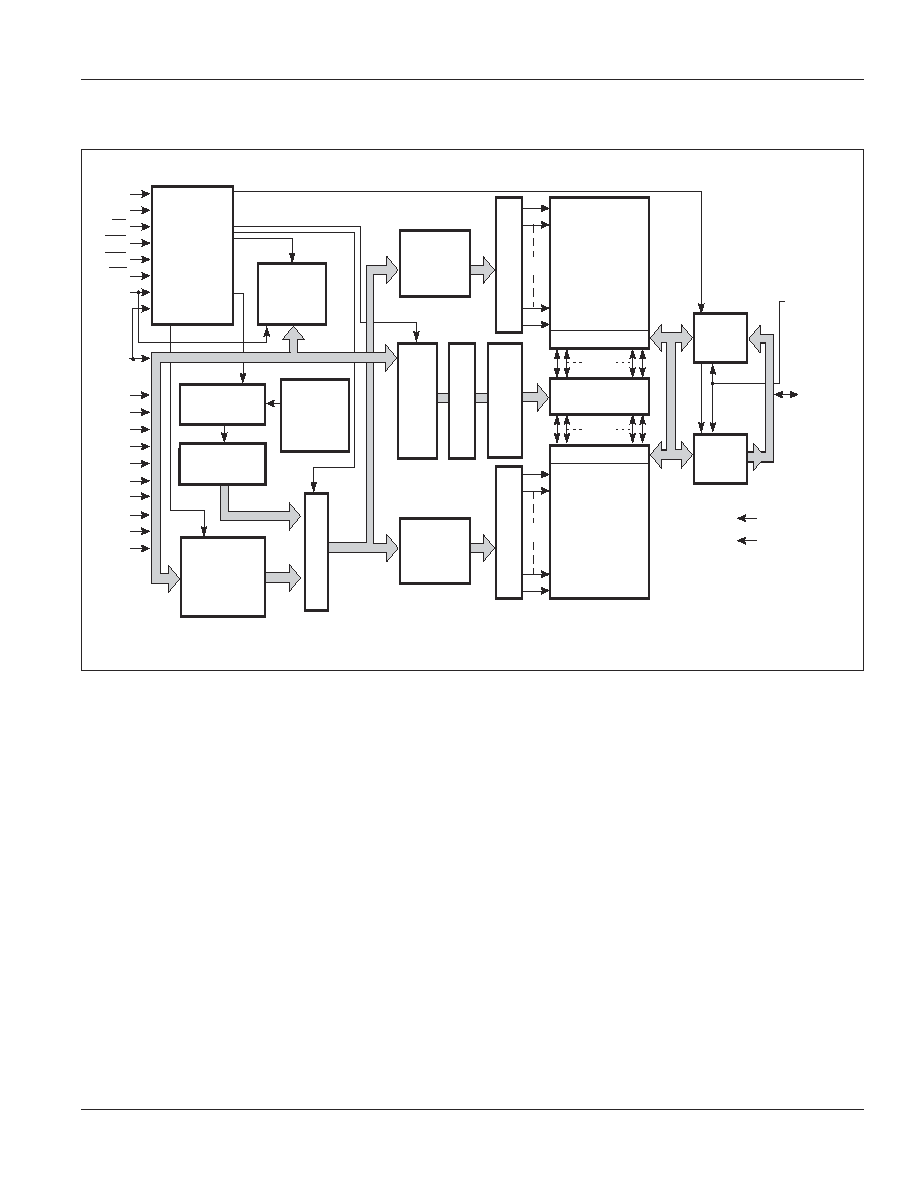
FUNCTIONAL BLOCK DIAGRAM
CLK
CKE
CS
RAS
CAS
WE
A11
A9
A8
A7
A6
A5
A4
A3
A2
A1
A0
A10
COMMAND
DECODER
&
CLOCK
GENERATOR
MODE
REGISTER
REFRESH
CONTROLLER
REFRESH
COUNTER
SELF
REFRESH
CONTROLLER
ROW
ADDRESS
LATCH
MUL
TIPLEXER
ROW
ADDRESS
BUFFER
ROW
ADDRESS
BUFFER
COLUMN
ADDRESS LA
TCH
B
U
RST COUNTER
COLUMN
ADDRESS B
U
FFER
R
O
W DECODER
R
O
W DECODER
MEMORY CELL
ARRAY
BANK 0
COLUMN DECODER
MEMORY CELL
ARRAY
BANK 1
DATA IN
BUFFER
DATA OUT
BUFFER
SENSE AMP I/O GATE
SENSE AMP I/O GATE
2048
2048
DQM
DQ 0-15
VDD/VDDQ
GND/GNDQ
11
11
11
11
8
11
11
8
16
16
16
16
256
256
S16BLK.eps
IS42S16100A2
ISSI
®
4
Integrated Silicon Solution, Inc. -- www.issi.com --
1-800-379-4774
Rev. A
04/16/03
ABSOLUTE MAXIMUM RATINGS
(1)
Symbol
Parameters
Rating
Unit
V
DD
MAX
Maximum Supply Voltage
1.0 to +4.6
V
V
DD
Q
MAX
Maximum Supply Voltage for Output Buffer
1.0 to +4.6
V
V
IN
Input Voltage
1.0 to +4.6
V
V
OUT
Output Voltage
1.0 to +4.6
V
P
D
MAX
Allowable Power Dissipation
1
W
I
CS
Output Shorted Current
50
mA
T
OPR
Operating Temperature
Com
0 to +70
°C
T
STG
Storage Temperature
55 to +150
°C
DC RECOMMENDED OPERATING CONDITIONS
(2)
(
At T
A
= 0°C to +70°C)
Symbol
Parameter
Min.
Typ.
Max.
Unit
V
DD
, V
DD
Q
Supply Voltage
3.0
3.3
3.6
V
V
IH
Input High Voltage
(3)
2.0
--
V
DD
+ 0.3
V
V
IL
Input Low Voltage
(4)
-0.3
--
+0.8
V
CAPACITANCE CHARACTERISTICS
(1,2)
(At T
A
= 0°C to +25°C, VDD = VDDQ = 3.3 ± 0.3V, f = 1 MHz)
Symbol
Parameter
Typ.
Max.
Unit
C
IN
1
Input Capacitance: A0-A11
--
4
pF
C
IN
2
Input Capacitance: (CLK, CKE,
CS
,
RAS
,
CAS
,
WE
, LDQM, UDQM)
--
4
pF
CI/O
Data Input/Output Capacitance: DQ0-DQ15
--
5
pF
Notes:
1. Stress greater than those listed under ABSOLUTE MAXIMUM RATINGS may cause permanent damage to the device. This
is a stress rating only and functional operation of the device at these or any other conditions above those indicated in the
operational sections of this specification is not implied. Exposure to absolute maximum rating conditions for extended
periods may affect reliability.
2. All voltages are referenced to GND.
3. V
IH
(max) = V
DDQ
+ 2.0V with a pulse width
3 ns.
4. V
IL
(min) = -1.5V with a pulse width
3 ns.
IS42S16100A2
ISSI
®
Integrated Silicon Solution, Inc. -- www.issi.com --
1-800-379-4774
5
Rev. A
04/16/03
DC ELECTRICAL CHARACTERISTICS
(Recommended Operation Conditions unless otherwise noted.)
Symbol Parameter
Test Condition
Speed
Min.
Max.
Unit
I
IL
Input Leakage Current
0V
V
IN
VDD, with pins other than
5
5
µA
the tested pin at 0V
I
OL
Output Leakage Current
Output is disabled, 0V
V
OUT
VDD
5
5
µA
V
OH
Output High Voltage Level I
OUT
= 2 mA
2.4
--
V
V
OL
Output Low Voltage Level
I
OUT
= +2 mA
--
0.4
V
I
CC1
Operating Current
(1,2)
One Bank Operation,
CAS
latency = 3
Burst Length=1
Com.
-7
--
160
mA
t
RC
t
RC
(min.)
Com.
-10
--
120
mA
I
OUT
= 0mA
I
CC2P
Precharge Standby Current CKE
V
IL
(
MAX
)
t
CK
= t
CK
(
MIN
) Com.
--
--
3
mA
t
CK
=
Com.
--
--
2
mA
I
CC2PS
(In Power-Down Mode)
I
CC3N
Active Standby Current
CKE
V
IH
(
MIN
)
t
CK
= t
CK
(
MIN
)
--
--
40
mA
I
CC3NS
(In Non Power-Down Mode)
t
CK
=
Com.
--
--
30
mA
I
CC4
Operating Current
t
CK
= t
CK
(
MIN
)
CAS
latency = 3
(In Burst Mode)
(1)
I
OUT
= 0mA
Com.
-7
--
180
mA
Com.
-10
--
140
mA
I
CC5
Auto-Refresh Current
t
RC
= t
RC
(
MIN
)
CAS
latency = 3
Com.
-7
--
180
mA
Com.
-10
--
140
mA
I
CC6
Self-Refresh Current
CKE
0.2V
--
---
1
mA
Notes:
1. These are the values at the minimum cycle time. Since the currents are transient, these values decrease as the cycle time
increases. Also note that a bypass capacitor of at least 0.01 µF should be inserted between V
DD
and GND for each
memory chip to suppress power supply voltage noise (voltage drops) due to these transient currents.
2. Icc
1
and Icc
4
depend on the output load. The maximum values for Icc
1
and Icc
4
are obtained with the output open state.