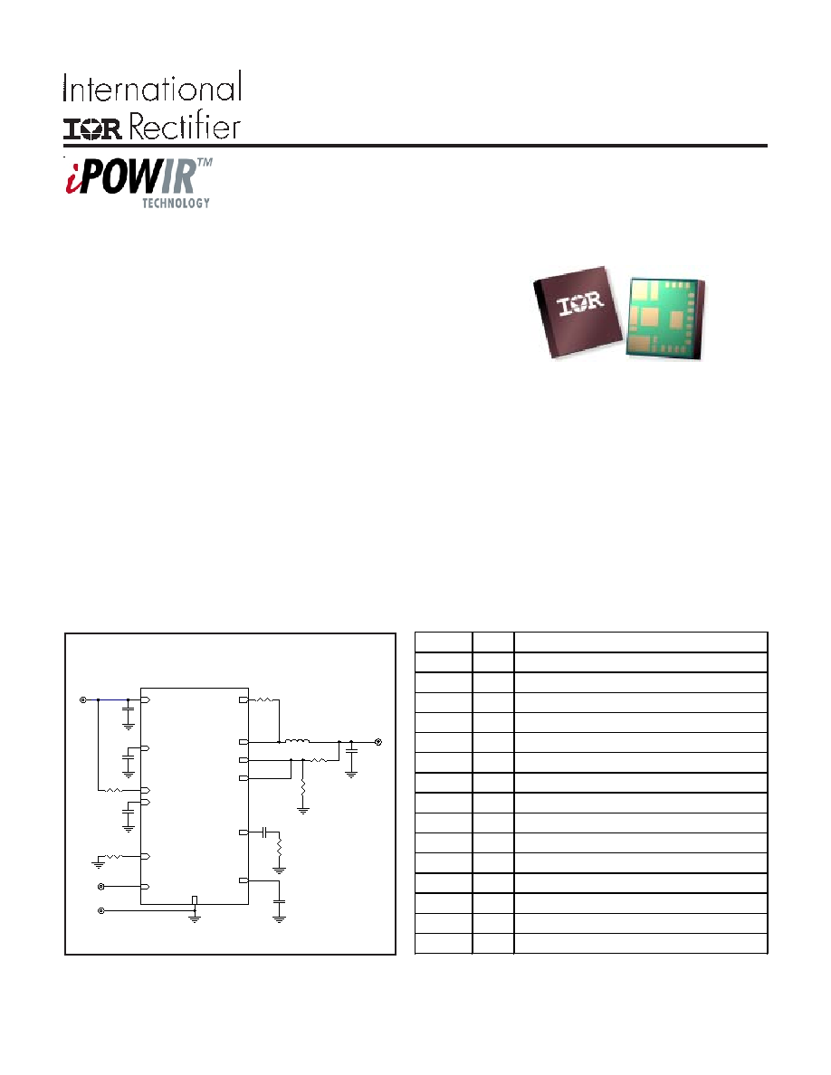
iP1203 Power Block
04/08/05
iP1203 Simplified Application Schematic
Description
The iP1203 is a fully optimized solution for medium current synchronous buck applications requiring up to 15A.
It includes full function PWM control, with optimized power semiconductor chipsets and associated passives,
achieving high power density. Very few external components are required to create a complete synchronous
buck power supply.
iPOWIR
TM
technology offers designers an innovative space-saving solution for applications requiring high
power densities. iPOWIR technology eases design for applications where component integration offers benefits
in performance and functionality. iPOWIR technology solutions are also optimized internally for layout, heat
transfer and component selection.
· 5.5V to 13.2V Input Voltage
· 0.8V to 8V Output Voltage
· 15A Maximum Load Capability
· 200-400kHz Nominal Switching Frequency
· Over Current Hiccup
· External Synchronization Capable
· Overvoltage Protection
· Over Temperature Protection
· Internal Features Minimize Layout Sensitivity
· Very Small Outline 9mm x 9mm x 2.3mm
Features
Single Output Full Function
Synchronous Buck Power Block
Integrated Power Semiconductors,
PWM Control & Passives
iP1203
V
SS
PG
N
D
FB
FB
CC
PGOOD
R
SYNC
OC
V
iP1203
V
SS
PG
N
D
FB
FB
CC
PGOOD
R
SYNC
OC
V
V
V
OUT
IN
CC_bypass
T
SW
REF
V
V
S
IN
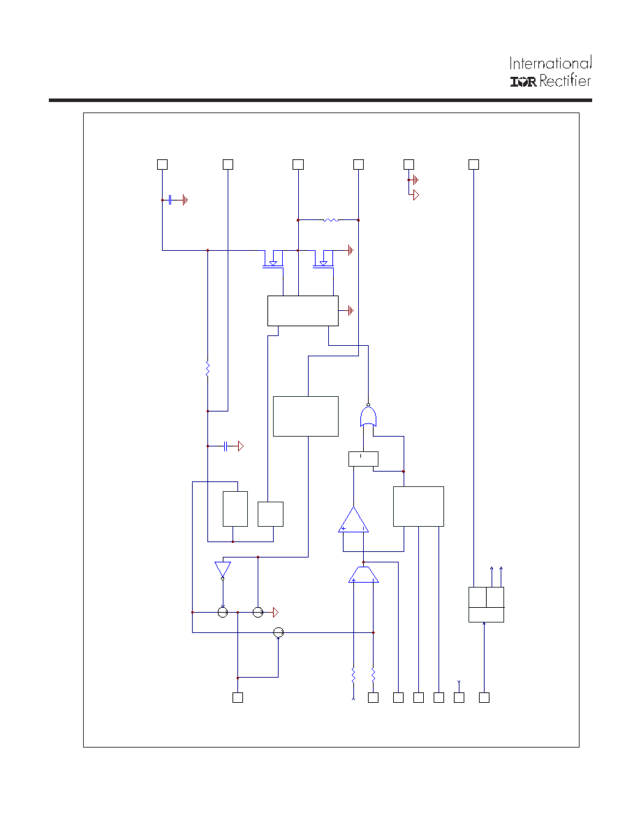
Pin Number
(See Page 18) Pin Name
Pin Description
1, 23
V
IN
Input voltage connection pins
2,3,4,5,7,17,20,21
PGND
Power Ground pins
6
V
CC_bypass
PWM controller power supply pin. Internally generated.
Requires a 2.2µf external bypass capacitor
8
SS
Soft start pin. External capacitor provides soft start. Pulling soft start pin low
will disable the output. Cannot be cycled to unlatch OVP trip
9
CC
Output of the error amplifier
10
FB
Inverting input of the error amplifier
11
FB
s
Output overvoltage sense pin.
12
R
T
Switching frequency setting pin. For R
T
selection, refer to Fig.9 of the
datasheet
13
PGOOD
Power Good pin. Open collector, requires external pulll-up. If function not
needed, pin can be left floating
14
V
REF
Non inverting input of the error amplifier (reference Voltage pin). Connect a
100pF cap from this pin to PGND.
15
SYNC
External Clock synchronization pin. Set free running frequency to 80% of
the SYNC frequency. When not in use, leave pin floating
16
OCSET
Output overcurrent trip threshold pin
18,19
V
SW
Output inductor connection pins
22
V
SWs
Test pad, for internal use, short to VSW
24
V
INs
Test pad, for internal use, short to V
IN
PD- 96921C