1
Û
FN9030.7
CAUTION: These devices are sensitive to electrostatic discharge; follow proper IC Handling Procedures.
1-888-INTERSIL or 321-724-7143
|
Intersil (and design) is a trademark of Intersil Americas Inc.
Copyright ˋ Intersil Americas Inc. 2001, 2002, 2004, 2005. All Rights Reserved
PowerPC
Û
is a trademark of IBM. AlphaPCTM is a trademark of Digital Equipment Corporation. Pentium
Û
is a registered trademark of Intel Corporation.
ISL6522
Buck and Synchronous Rectifier
Pulse-Width Modulator (PWM) Controller
The ISL6522 provides complete control and protection for a
DC-DC converter optimized for high-performance micro-
processor applications. It is designed to drive two N-Channel
MOSFETs in a synchronous rectified buck topology. The
ISL6522 integrates all of the control, output adjustment,
monitoring and protection functions into a single package.
The output voltage of the converter can be precisely
regulated to as low as 0.8V, with a maximum tolerance of
Ý1% over temperature and line voltage variations.
The ISL6522 provides simple, single feedback loop, voltage-
mode control with fast transient response. It includes a
200kHz free-running triangle-wave oscillator that is
adjustable from below 50kHz to over 1MHz. The error
amplifier features a 15MHz gain-bandwidth product and
6V/
çs slew rate which enables high converter bandwidth for
fast transient performance. The resulting PWM duty ratio
ranges from 0Ù100%.
The ISL6522 protects against overcurrent conditions by
inhibiting PWM operation. The ISL6522 monitors the current
by using the r
DS(ON)
of the upper MOSFET which eliminates
the need for a current sensing resistor.
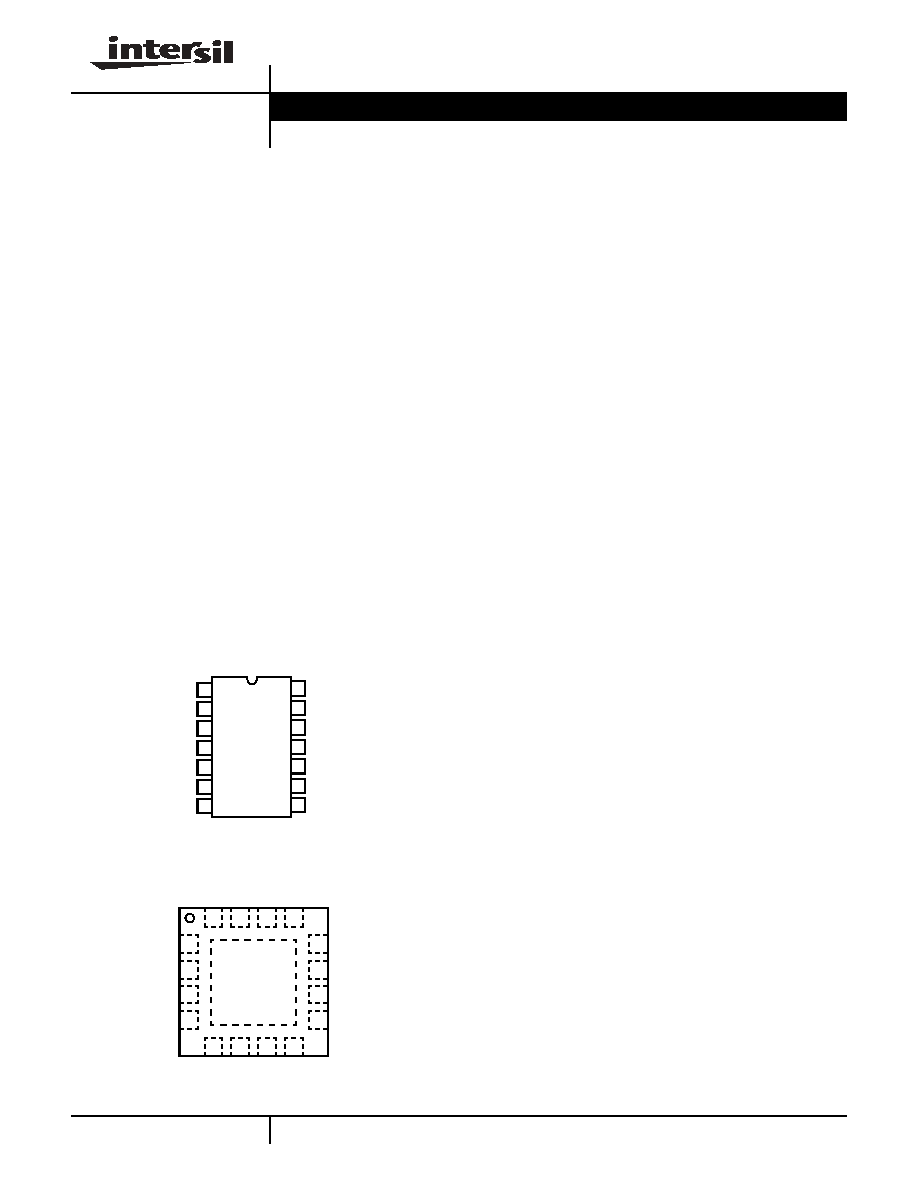
Pinouts
SOIC, TSSOP
TOP VIEW
QFN
TOP VIEW
Features
ñ Drives two N-Channel MOSFETs
ñ Operates from +5V or +12V input
ñ Simple single-loop control design
- Voltage-mode PWM control
ñ Fast transient response
- High-bandwidth error amplifier
- Full 0Ù100% duty ratio
ñ Excellent output voltage regulation
- 0.8V internal reference
-
Ý1% over line voltage and temperature
ñ Overcurrent fault monitor
- Does not require extra current sensing element
- Uses MOSFETs r
DS(ON)
ñ Converter can source and sink current
ñ Small converter size
- Constant frequency operation
- 200kHz free-running oscillator programmable from
50kHz to over 1MHz
ñ 14-lead SOIC and TSSOP package and 16-lead 5x5mm
QFN Package
ñ QFN Package
- Compliant to JEDEC PUB95 MO-220 QFN-Quad Flat
No Leads-Product Outline.
- Near Chip-Scale Package Footprint; Improves PCB
Efficiency and Thinner in Profile
ñ Pb-Free Available (RoHS Compliant)
Applications
ñ Power supply for Pentium
Û
, Pentium Pro, PowerPC
Û
and
AlphaPCTM microprocessors
ñ High-power 5V to 3.xV DC-DC regulators
ñ Low-voltage distributed power supplies
8
9
10
11
12
13
14
7
6
5
4
3
2
1
OCSET
SS
EN
COMP
FB
RT
VCC
LGATE
PGND
BOOT
UGATE
PHASE
GND
PVCC
1
3
4
15
SS
COMP
FB
EN
NC
OCSE
T
RT
VCC
16
14
13
2
12
10
9
11
6
5
7
8
PVCC
LGATE
PGND
BOOT
NC
GND
PHASE
UGA
T
E
GND
Data Sheet
March 4, 2005

2
FN9030.7
March 4, 2005
Typical Application
Block Diagram
Ordering Information
PART NUMBER
TEMP.
RANGE (¯C)
PACKAGE
PKG.
DWG. #
ISL6522CB
0 to 70
14 Ld SOIC
M14.15
ISL6522CBZ (Note)
0 to 70
14 Ld SOIC (Pb-free) M14.15
ISL6522CBZA
(Note)
0 to 70
14 Ld SOIC (Pb-free) M14.15
ISL6522IB
-40 to 85
14 Ld SOIC
M14.15
ISL6522IBZ (Note)
-40 to 85
14 Ld SOIC (Pb-free) M14.15
ISL6522CV
0 to 70
14 Ld TSSOP
M14.173
ISL6522CVZ
(Note)
0 to 70
14 Ld TSSOP
(Pb-free)
M14.173
ISL6522IV
-40 to 85
14 Ld TSSOP
M14.173
ISL6522IVZ (Note)
-40 to 85
14 Ld TSSOP
(Pb-free)
M14.173
ISL6522CR
0 to 70
16 Ld 5x5 QFN
L16.5x5B
ISL6522CRZ
(Note)
0 to 70
16 Ld 5x5 QFN
(Pb-free)
L16.5x5B
ISL6522IR
-40 to 85
16 Ld 5x5 QFN
L16.5x5B
ISL6522IRZ (Note)
-40 to 85
16 Ld 5x5 QFN
(Pb-free)
L16.5x5B
NOTE: Intersil Pb-free products employ special Pb-free material sets;
molding compounds/die attach materials and 100% matte tin plate
termination finish, which are RoHS compliant and compatible with
both SnPb and Pb-free soldering operations. Intersil Pb-free products
are MSL classified at Pb-free peak reflow temperatures that meet or
exceed the Pb-free requirements of IPC/JEDEC J STD-020C.
Add "-T" for tape and reel.
Ordering Information
(Continued)
PART NUMBER
TEMP.
RANGE (¯C)
PACKAGE
PKG.
DWG. #
12V
+V
O
PGND
ISL6522
R
T
FB
COMP
SS
GND
OSC
LGATE
UGATE
OCSET
PHASE
BOOT
EN
V
CC
+5V OR +12V
PV
CC
+12V
MONITOR AND
PROTECTION
REF
+
-
+
-
OSCILLATOR
SOFT-
START
POWER-ON
RESET (POR)
INHIBIT
PWM
COMPARATOR
ERROR
AMP
V
CC
SS
PWM
R
T
GND
OCSET
FB
COMP
EN
0.8V
REF
OVER
CURRENT
GATE
CONTROL
LOGIC
BOOT
UGATE
LGATE
PHASE
PGND
200
çA
PV
CC
10
çA
4V
REFERENCE
+
-
+
-
+
-
ISL6522

3
FN9030.7
March 4, 2005
Absolute Maximum Ratings
Thermal Information
Supply Voltage, V
CC
. . . . . . . . . . . . . . . . . . . . . . . . . . . . . . . +15.0V
Boot Voltage, V
BOOT
- V
PHASE
. . . . . . . . . . . . . . . . . . . . . . +15.0V
Input, Output or I/O Voltage . . . . . . . . . . . . GND -0.3V to V
CC
+0.3V
ESD Classification . . . . . . . . . . . . . . . . . . . . . . . . . . . . . . . . . Class 2
Recommended Operating Conditions
Supply Voltage, V
CC
. . . . . . . . . . . . . . . . . . . . . . . . . . . +12V
Ý10%
Ambient Temperature Range, ISL6522C . . . . . . . . . . . . 0¯C to 70¯C
Ambient Temperature Range, ISL6522I. . . . . . . . . . . .-40¯C to 85¯C
Junction Temperature Range, ISL6522C. . . . . . . . . . . 0¯C to 125¯C
Junction Temperature Range, ISL6522I . . . . . . . . . .-40¯C to 125¯C
Thermal Resistance (Typical, Note 1)
JA
(¯C/W)
JC
(¯C/W)
SOIC Package (Note 1) . . . . . . . . . . . .
67
n/a
TSSOP Package (Note 1) . . . . . . . . . .
95
n/a
QFN Package (Notes 2, 3). . . . . . . . . .
36
5
Maximum Junction Temperature . . . . . . . . . . . . . . . . . . . . . . 150¯C
Maximum Storage Temperature Range . . . . . . . . . . . -65¯C to 150¯C
Maximum Lead Temperature (Soldering 10s) . . . . . . . . . . . . 300¯C
(SOIC - Lead Tips Only)
CAUTION: Stresses above those listed in "Absolute Maximum Ratings" may cause permanent damage to the device. This is a stress only rating and operation of the
device at these or any other conditions above those indicated in the operational sections of this specification is not implied.
NOTES:
1.
JA
is measured with the component mounted on a highs effective thermal conductivity test board in free air. See Tech Brief TB379 for details.
2.
JA
is measured in free air with the component mounted on a high effective thermal conductivity test board with "direct attach" features. SeeTech
Brief TB379.
3. For
JC
, the "case temp" location is the center of the exposed metal pad on the package underside.
Electrical Specifications
Recommended Operating Conditions, Unless Otherwise Noted
PARAMETER
SYMBOL
TEST CONDITIONS
MIN
TYP
MAX
UNITS
V
CC
SUPPLY CURRENT
Nominal Supply
I
CC
EN = V
CC
; UGATE and LGATE Open
-
5
-
mA
Shutdown Supply
EN = 0V
-
50
100
çA
POWER-ON RESET
Rising V
CC
Threshold
V
OCSET
= 4.5VDC
-
-
10.4
V
Falling V
CC
Threshold
V
OCSET
= 4.5VDC
8.1
-
-
V
Enable-Input Threshold Voltage
ISL6522C, V
OCSET
= 4.5VDC
0.8
-
2.0
V
ISL6522I, V
OCSET
= 4.5VDC
0.8
-
2.1
V
Rising V
OCSET
Threshold
-
1.27
-
V
OSCILLATOR
Free Running Frequency
ISL6522C, R
T
= OPEN, V
CC
= 12
175
200
230
kHz
ISL6522I, R
T
= OPEN, V
CC
= 12
160
200
230
Total Variation
6k
< R
T
to GND < 200k
-20
-
+20
%
Ramp Amplitude
V
OSC
R
T
= OPEN
-
1.9
-
V
P-P
REFERENCE
Reference Voltage Tolerance
V
REF
Commercial
-1
-
1
%
Industrial
-2
-
+1
%
Reference Voltage
-
0.800
-
V
ERROR AMPLIFIER
DC Gain
-
88
-
dB
Gain-Bandwidth Product
GBW
-
15
-
MHz
Slew Rate
SR
COMP = 10pF
-
6
-
V/
çs
GATE DRIVERS
Upper Gate Source
I
UGATE
V
BOOT
- V
PHASE
= 12V, V
UGATE
= 6V
350
500
-
mA
ISL6522

4
FN9030.7
March 4, 2005
Functional Pin Descriptions
RT
This pin provides oscillator switching frequency adjustment.
By placing a resistor (R
T
) from this pin to GND, the nominal
200kHz switching frequency is increased according to the
following equation:
Conversely, connecting a pull-up resistor (R
T
) from this pin
to V
CC
reduces the switching frequency according to the
following equation:
Upper Gate Sink
R
UGATE
ISL6522C, I
LGATE
= 0.3A
-
5.5
10
ISL6522I, I
LGATE
= 0.3A
-
5.5
7.2
Lower Gate Source
I
LGATE
V
CC
= 12V, V
LGATE
= 6V
300
450
-
mA
Lower Gate Sink
R
LGATE
ISL6522C, I
LGATE
= 0.3A
-
3.5
6.5
ISL6522I, I
LGATE
= 0.3A
-
3.5
4.5
PROTECTION
OCSET Current Source
I
OCSET
V
OCSET
= 4.5VDC
170
200
230
çA
Soft-Start Current
I
SS
-
10
-
çA
Electrical Specifications
Recommended Operating Conditions, Unless Otherwise Noted (Continued)
PARAMETER
SYMBOL
TEST CONDITIONS
MIN
TYP
MAX
UNITS
Typical Performance Curves
FIGURE 1. R
T
RESISTANCE vs FREQUENCY
FIGURE 2. BIAS SUPPLY CURRENT vs FREQUENCY
10
100
1000
SWITCHING FREQUENCY (kHz)
RESISTANCE (k
)
10
100
1000
R
T
PULLUP
TO +12V
R
T
PULLDOWN
TO V
SS
100
200
300
400
500
600
700
800
900
1000
80
70
60
50
40
30
20
10
0
I
VC
C
(mA)
SWITCHING FREQUENCY (kHz)
C
GATE
= 1000pF
C
GATE
= 3300pF
C
GATE
= 10pF
8
9
10
11
12
13
14
7
6
5
4
3
2
1
OCSET
SS
EN
COMP
FB
RT
VCC
LGATE
PGND
BOOT
UGATE
PHASE
GND
PVCC
SOIC
and
TSSOP
QFN
1
3
4
15
SS
COMP
FB
EN
NC
OC
SE
T
RT
VCC
16
14
13
2
12
10
9
11
6
5
7
8
PVCC
LGATE
PGND
BOOT
NC
GND
PH
ASE
UG
A
T
E
GND
Fs 200kHz 5 10
6
ñ
R
T
------------------
+
(R
T
to GND)
Fs 200kHz 4 10
7
ñ
R
T
------------------
Ù
(R
T
to 12V)
ISL6522

5
FN9030.7
March 4, 2005
OCSET
Connect a resistor (R
OCSET
) from this pin to the drain of the
upper MOSFET. R
OCSET
, an internal 200
çA current source
(I
OCS
), and the upper MOSFET on-resistance (r
DS(ON)
) set
the converter overcurrent (OC) trip point according to the
following equation:
An overcurrent trip cycles the soft-start function.
SS
Connect a capacitor from this pin to ground. This capacitor,
along with an internal 10
çA current source, sets the soft-start
interval of the converter.
COMP and FB
COMP and FB are the available external pins of the error
amplifier. The FB pin is the inverting input of the error
amplifier and the COMP pin is the error amplifier output.
These pins are used to compensate the voltage-control
feedback loop of the converter.
EN
This pin is the open-collector enable pin. Pull this pin below
1V to disable the converter. In shutdown, the soft-start pin is
discharged and the UGATE and LGATE pins are held low.
GND
Signal ground for the IC. All voltage levels are measured
with respect to this pin.
PHASE
Connect the PHASE pin to the upper MOSFET source. This
pin is used to monitor the voltage drop across the MOSFET
for overcurrent protection. This pin also provides the return
path for the upper gate drive.
UGATE
Connect UGATE to the upper MOSFET gate. This pin
provides the gate drive for the upper MOSFET. This pin is also
monitored by the adaptive shoot through protection circuitry to
determine when the upper MOSFET has turned off.
BOOT
This pin provides bias voltage to the upper MOSFET driver.
A bootstrap circuit may be used to create a BOOT voltage
suitable to drive a standard N-Channel MOSFET.
PGND
This is the power ground connection. Tie the lower MOSFET
source to this pin.
LGATE
Connect LGATE to the lower MOSFET gate. This pin provides
the gate drive for the lower MOSFET. This pin is also
monitored by the adaptive shoot through protection circuitry to
determine when the lower MOSFET has turned off.
PVCC
Provide a bias supply for the lower gate drive to this pin.
VCC
Provide a 12V bias supply for the chip to this pin.
Functional Description
Initialization
The ISL6522 automatically initializes upon receipt of power.
Special sequencing of the input supplies is not necessary.
The Power-On Reset (POR) function continually monitors
the input supply voltages and the enable (EN) pin. The POR
monitors the bias voltage at the VCC pin and the input
voltage (V
IN
) on the OCSET pin. The level on OCSET is
equal to V
IN
Less a fixed voltage drop (see overcurrent
protection). With the EN pin held to V
CC
, the POR function
initiates soft-start operation after both input supply voltages
exceed their POR thresholds. For operation with a single
+12V power source, V
IN
and V
CC
are equivalent and the
+12V power source must exceed the rising V
CC
threshold
before POR initiates operation.
The POR function inhibits operation with the chip disabled
(EN pin low). With both input supplies above their POR
thresholds, transitioning the EN pin high initiates a soft-start
interval.
Soft-Start
The POR function initiates the soft-start sequence. An internal
10
çA current source charges an external capacitor (C
SS
) on
the SS pin to 4V. Soft-start clamps the error amplifier output
(COMP pin) to the SS pin voltage. Figure 3 shows the soft-
start interval. At t
1
in Figure 3, the SS and COMP voltages
reach the valley of the oscillator's triangle wave. The
oscillator's triangular waveform is compared to the ramping
error amplifier voltage. This generates PHASE pulses of
increasing width that charge the output capacitor(s). This
interval of increasing pulse width continues to t2, at which
point the output is in regulation and the clamp on the COMP
pin is released. This method provides a rapid and controlled
output voltage rise.
I
PEAK
I
OCS
R
OCSET
ñ
r
DS ON
(
)
--------------------------------------------
=
ISL6522