
1
®
ISL12026
Real Time Clock/Calendar with EEPROM
The ISL12026 device is a micro power real time clock with
timing and crystal compensation, clock/calender, power-fail
indicator, two periodic or polled alarms, intelligent battery
backup switching, and integrated 512 x 8bit EEPROM
configured in 16 Byte per page.
The oscillator uses an external, low-cost 32.768kHz crystal.
The real time clock tracks time with separate registers for
hours, minutes, and seconds. The device has calendar
registers for date, month, year and day of the week. The
calendar is accurate through 2099, with automatic leap year
correction.
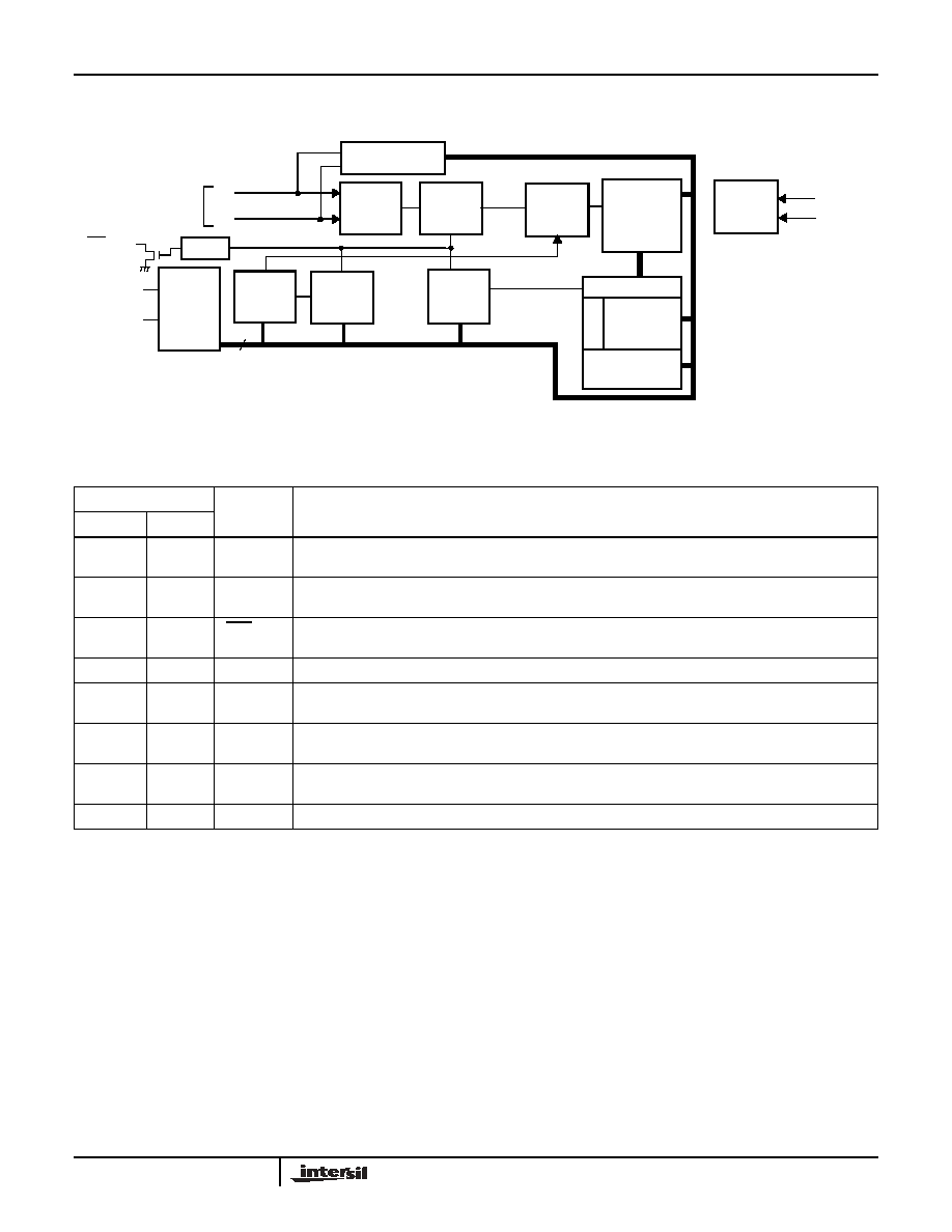
Pinouts
Features
· Real Time Clock/Calendar
- Tracks time in Hours, Minutes, and Seconds
- Day of the Week, Day, Month, and Year
- 3 Selectable Frequency Outputs
· Two Non-Volatile Alarms
- Settable on the Second, Minute, Hour, Day of the Week,
Day, or Month
- Repeat Mode (periodic interrupts)
· Automatic Backup to Battery or SuperCap
· On-Chip Oscillator Compensation
- Internal Feedback Resistor and Compensation
Capacitors
- 64 Position Digitally Controlled Trim Capacitor
- 6 Digital Frequency Adjustment Settings to ±30ppm
· 512 x 8 Bits of EEPROM
- 16-Byte Page Write Mode (32 total pages)
- 8 Modes of BlockLockTM
Protection
- Single Byte Write Capability
· High Reliability
- Data Retention: 50 years
- Endurance: >2,000,000 Cycles Per Byte
· I
2
C Interface
- 400kHz Data Transfer Rate
· 800nA Battery Supply Current
· Package Options
- 8 Ld SOIC and TSSOP Packages
· Pb-Free Plus Anneal Available (RoHS Compliant)
Applications
· Utility Meters
· HVAC Equipment
· Audio/Video Components
· Set Top Box/Television
· Modems
· Network Routers, Hubs, Switches, Bridges
· Cellular Infrastructure Equipment
· Fixed Broadband Wireless Equipment
· Pagers/PDA
· POS Equipment
· Test Meters/Fixtures
· Office Automation (Copiers, Fax)
· Home Appliances
· Computer Products
· Other Industrial/Medical/Automotive
Ordering Information
PART
NUMBER
PART
MARKING
V
DD
RANGE
TEMP
RANGE
(°C)
PACKAGE
PKG.
DWG. #
ISL12026IBZ
(See Note)
12026IBZ
2.7V to
5.5V
-40 to +85 8 Ld SOIC
(Pb-Free)
M8.15
ISL12026IVZ
(See Note)
2026IVZ
2.7V to
5.5V
-40 to +85 8 Ld TSSOP
(Pb-Free)
M8.173
NOTE: Intersil Pb-free plus anneal products employ special Pb-free
material sets; molding compounds/die attach materials and 100%
matte tin plate termination finish, which are RoHS compliant and
compatible with both SnPb and Pb-free soldering operations. Intersil
Pb-free products are MSL classified at Pb-free peak reflow
temperatures that meet or exceed the Pb-free requirements of IPC/
JEDEC J STD-020.
Add "-T" suffix for tape and reel.
X1
X2
V
BAT
V
DD
IRQ/F
OUT
SCL
SDA
GND
1
2
3
4
7
8
6
5
8 LD SOIC
X1
X2
V
BAT
V
DD
IRQ/F
OUT
SCL
SDA
GND
1
2
3
4
7
8
6
5
8 LD TSSOP
New Features
Data Sheet
FN8231.3
April 13, 2006
CAUTION: These devices are sensitive to electrostatic discharge; follow proper IC Handling Procedures.
1-888-INTERSIL or 1-888-468-3774
|
Intersil (and design) is a registered trademark of Intersil Americas Inc.
BlockLock is a trademark of Intersil Americas Inc. Copyright Intersil Americas Inc. 2005, 2006. All Rights Reserved
All other trademarks mentioned are the property of their respective owners.
2
FN8231.3
April 13, 2006
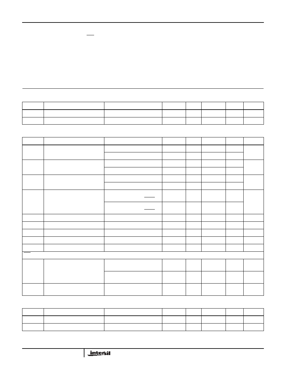
Block Diagram
X1
X2
OSCILLATOR
FREQUENCY
TIMER
LOGIC
DIVIDER
CALENDAR
8
CONTROL/
REGISTERS
1Hz
TIME
KEEPING
REGISTERS
ALARM REGS
COMPARE
MA
S
K
CONTROL
DECODE
LOGIC
ALARM
(EEPROM)
(EEPROM)
SCL
SDA
SERIAL
INTERFACE
DECODER
4K
EEPROM
ARRAY
REGISTERS
STATUS
(SRAM)
SELECT
IRQ/F
OUT
V
DD
V
BAT
32.768kHz
(SRAM)
BATTERY
CIRCUITRY
SWITCH
OSC
COMPENSATION
Pin Descriptions
PIN NUMBER
SYMBOL
DESCRIPTION
SOIC
TSSOP
1
3
X1
The X1 pin is the input of an inverting amplifier and is intended to be connected to one pin of an external
32.768kHz quartz crystal. X1 can also be driven directly from a 32.768kHz source. (See Application Section)
2
4
X2
The X2 pin is the output of an inverting amplifier and is intended to be connected to one pin of an external
32.768kHz quartz crystal. (See Application Section)
3
5
IRQ/F
OUT
Interrupt Output/Frequency Output is a multi-functional pin that can be used as interrupt or frequency
output pin. The function is set via the control register. This output is an open drain configuration.
4
6
GND
Ground.
5
7
SDA
Serial Data (SDA) is a bidirectional pin used to transfer serial data into and out of the device. It has an open
drain output and may be wire OR'ed with other open drain or open collector outputs.
6
8
SCL
The Serial Clock (SCL) input is used to clock all serial data into and out of the device. The input buffer on
this pin is always active (not gated).
7
1
V
BAT
This input provides a backup supply voltage to the device. V
BAT
supplies power to the device in the event
that the V
DD
supply fails. This pin should be tied to ground if not used.
8
2
V
DD
Power Supply.
ISL12026
3
FN8231.3
April 13, 2006
Absolute Maximum Ratings
Thermal Information
Voltage on V
DD
, V
BAT
, SCL, SDA, and
IRQ/F
OUT Pins
(respect to ground) . . . . . . . . . . . . . . . . . . . . . . . . . . -0.3V to 6.0V
Voltage on X1 and X2 Pins
(respect to ground) . . . . . . . . . . . . . . . . . . . . . . . . . . -0.3V to 2.5V
ESD Rating (MIL-STD-883, Method 3014) . . . . . . . . . . . . . . .>±2kV
ESD Rating (Machine Model) . . . . . . . . . . . . . . . . . . . . . . . . .>175V
Thermal Resistance (Note)
JA
(°C/W)
8 Ld SOIC Package . . . . . . . . . . . . . . . . . . . . . . . . .
120
8 Ld TSSOP Package . . . . . . . . . . . . . . . . . . . . . . .
140
Storage Temperature . . . . . . . . . . . . . . . . . . . . . . . .-65°C to +150°C
Lead Temperature (Soldering, 10s) . . . . . . . . . . . . . . . . . . . . . 300°C
CAUTION: Stresses above those listed in "Absolute Maximum Ratings" may cause permanent damage to the device. This is a stress only rating and operation of the
device at these or any other conditions above those indicated in the operational sections of this specification is not implied.
NOTE:
JA
is measured with the component mounted on a high effective thermal conductivity test board in free air. See Tech Brief TB379 for details.
DC Operating Specifications
Unless otherwise noted, V
DD
= +2.7V to +5.5V, T
A
= -40°C to +85°C, Typical values are @ T
A
= 25°C and
V
DD
= 3.3V
SYMBOL
PARAMETER
CONDITIONS
MIN
TYP
MAX
UNIT
NOTES
V
DD
Main Power Supply
2.7
5.5
V
V
BAT
Backup Power Supply
1.8
5.5
V
Electrical Specifications
SYMBOL
PARAMETER
CONDITIONS
MIN
TYP
MAX
UNIT
NOTES
I
DD1
Supply Current with I
2
C Active
V
DD
= 2.7V
500
µA
1, 2, 3
V
DD
= 5.5V
800
µA
I
DD2
Supply Current for Non-Volatile
Programming
V
DD
= 2.7V
2.5
mA
1, 2, 3
V
DD
= 5.5V
3.5
mA
I
DD3
Supply Current for Main
Timekeeping (Low Power Mode)
V
DD
= V
SDA
= V
SCL
= 2.7V
10
µA
3
V
DD
= V
SDA
= V
SCL
= 5.5V
20
µA
I
BAT
Battery Supply Current
V
BAT
= 1.8V,
V
DD
= V
SDA
= V
SCL
= V
RESET
= 0
800
1000
nA
1, 4, 5
V
BAT
= 3.0V,
V
DD
= V
SDA
= V
SCL
= V
RESET
= 0
850
1200
nA
I
BATLKG
Battery Input Leakage
V
DD
= 5.5V, V
BAT
= 1.8V
100
nA
V
TRIP
V
BAT
Mode Threshold
1.8
2.2
2.6
V
5
V
TRIPHYS
V
TRIP
Hysteresis
30
mV
5, 8
V
BATHYS
V
BAT
Hysteresis
50
mV
5, 8
V
DD SR-
V
DD
Negative Slew Rate
10
V/ms
6
IRQ/F
OUT
V
OL
Output Low Voltage
V
DD
= 5V
I
OL
= 3mA
0.4
V
V
DD
= 1.8V
I
OL
= 1mA
0.4
V
I
LO
Output Leakage Current
V
DD
= 5.5V
V
OUT
= 5.5V
100
400
nA
EEPROM Specifications
SYMBOL
PARAMETER
TEST CONDITIONS
MIN
TYP
MAX
UNITS
NOTES
EEPROM Endurance
>2,000,000
Cycles
EEPROM Retention
Temperature
75°C
50
Years
ISL12026
4
FN8231.3
April 13, 2006
Serial Interface (I
2
C) Specifications
DC Electrical Specifications
SYMBOL
PARAMETER
TEST CONDITIONS
MIN
TYP
MAX
UNITS
NOTES
V
IL
SDA, and SCL Input Buffer LOW
Voltage
-0.3
0.3 x V
DD
V
V
IH
SDA, and SCL Input Buffer HIGH
Voltage
0.7 x V
DD
V
DD
+ 0.3
V
Hysteresis SDA and SCL Input Buffer
Hysteresis
0.05 x V
DD
V
V
OL
SDA Output Buffer LOW Voltage
I
OL
= 4mA
0
0.4
V
I
LI
Input Leakage Current on SCL
V
IN
= 5.5V
100
nA
I
LO
I/O Leakage Current on SDA
V
IN
= 5.5V
100
nA
AC Electrical Specifications
SYMBOL
PARAMETER
TEST CONDITIONS
MIN
TYP
MAX
UNITS
NOTES
f
SCL
SCL Frequency
400
kHz
t
IN
Pulse width Suppression Time at
SDA and SCL Inputs
Any pulse narrower than the max
spec is suppressed.
50
ns
t
AA
SCL Falling Edge to SDA Output
Data Valid
SCL falling edge crossing 30% of
V
DD
, until SDA exits the 30% to
70% of V
DD
window.
900
ns
t
BUF
Time the Bus Must be Free Before
the Start of a New Transmission
SDA crossing 70% of V
DD
during
a STOP condition, to SDA
crossing 70% of V
DD
during the
following START condition.
1300
ns
t
LOW
Clock LOW Time
Measured at the 30% of V
DD
crossing.
1300
ns
t
HIGH
Clock HIGH Time
Measured at the 70% of V
DD
crossing.
600
ns
t
SU:STA
START Condition Setup Time
SCL rising edge to SDA falling
edge. Both crossing 70% of V
DD
.
600
ns
t
HD:STA
START Condition Hold Time
From SDA falling edge crossing
30% of V
DD
to SCL falling edge
crossing 70% of V
DD
.
600
ns
t
SU:DAT
Input Data Setup Time
From SDA exiting the 30% to
70% of V
DD
window, to SCL rising
edge crossing 30% of V
DD
.
100
ns
t
HD:DAT
Input Data Hold Time
From SCL rising edge crossing
70% of V
DD
to SDA entering the
30% to 70% of V
DD
window.
0
ns
t
SU:STO
STOP Condition Setup Time
From SCL rising edge crossing
70% of V
DD
, to SDA rising edge
crossing 30% of V
DD
.
600
ns
t
HD:STO
STOP Condition Hold Time for
Read, or Volatile Only Write
From SDA rising edge to SCL
falling edge. Both crossing 70%
of V
DD
.
600
ns
t
DH
Output Data Hold Time
From SCL falling edge crossing
30% of V
DD
, until SDA enters the
30% to 70% of V
DD
window.
0
ns
Cb
Capacitive Loading of SDA or SCL Total on-chip and off-chip.
10
400
pF
ISL12026
5
FN8231.3
April 13, 2006
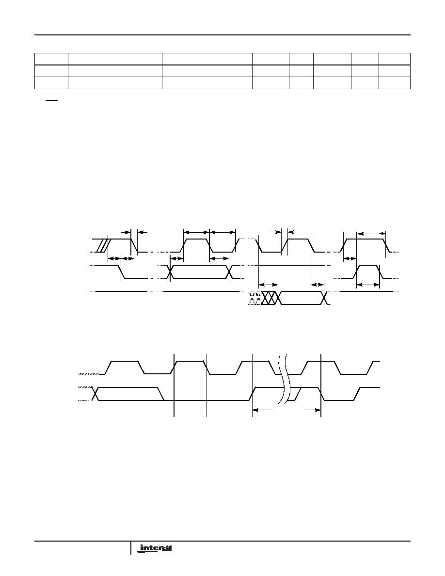
Timing Diagrams
Bus Timing
Write Cycle Timing
Cpin
SDA, and SCL Pin Capacitance
10
pF
t
WC
Non-volatile Write Cycle Time
12
20
ms
8
NOTES:
1. IRQ/F
OUT
Inactive.
2. V
IL
= V
DD
x 0.1, V
IH
= V
DD
x 0.9, f
SCL
= 400kHz
3. V
DD
> V
BAT
+V
BATHYS
4. Bit BSW = 0 (Standard Mode), V
BAT
>= 1.8V
5. Specified at 25°C.
6. In order to ensure proper timekeeping, the V
DD SR-
specification must be followed.
7. Parameter is not 100% tested.
8. t
WC
is the minimum cycle time to be allowed for any non-volatile Write by the user, it is the time from valid STOP condition at the end of Write
sequence of a serial interface Write operation, to the end of the self-timed internal non-volatile write cycle.
AC Electrical Specifications
(Continued)
SYMBOL
PARAMETER
TEST CONDITIONS
MIN
TYP
MAX
UNITS
NOTES
t
SU:STO
t
DH
t
HIGH
t
SU:STA
t
HD:STA
t
HD:DAT
t
SU:DAT
SCL
SDA
(INPUT TIMING)
SDA
(OUTPUT TIMING)
t
F
t
LOW
t
BUF
t
AA
t
R
t
HD:STO
SCL
SDA
t
WC
8TH BIT OF LAST BYTE
ACK
STOP
CONDITION
START
CONDITION
ISL12026