
1
«
FN3082.7
ICL7106, ICL7107, ICL7107S
3
1
/
2
Digit, LCD/LED Display, A/D
Converters
The Intersil ICL7106 and ICL7107 are high performance, low
power, 3
1
/
2
digit A/D converters. Included are seven
segment decoders, display drivers, a reference, and a clock.
The ICL7106 is designed to interface with a liquid crystal
display (LCD) and includes a multiplexed backplane drive;
the ICL7107 will directly drive an instrument size light
emitting diode (LED) display.
The ICL7106 and ICL7107 bring together a combination of
high accuracy, versatility, and true economy. It features auto-
zero to less than 10
Ą
V, zero drift of less than 1
Ą
V/
o
C, input
bias current of 10pA (Max), and rollover error of less than
one count. True differential inputs and reference are useful in
all systems, but give the designer an uncommon advantage
when measuring load cells, strain gauges and other bridge
type transducers. Finally, the true economy of single power
supply operation (ICL7106), enables a high performance
panel meter to be built with the addition of only 10 passive
components and a display.
Features
Ę Guaranteed Zero Reading for 0V Input on All Scales
Ę True Polarity at Zero for Precise Null Detection
Ę 1pA Typical Input Current
Ę True Differential Input and Reference, Direct Display Drive
- LCD ICL7106, LED lCL7107
Ę Low Noise - Less Than 15
Ą
V
P-P
Ę On Chip Clock and Reference
Ę Low Power Dissipation - Typically Less Than 10mW
Ę No Additional Active Circuits Required
Ę Enhanced Display Stability
Ę Pb-Free Plus Anneal Available (RoHS Compliant)
Ordering Information
PART NO.
PART MARKING
TEMP. RANGE
(░C)
PACKAGE
PKG. DWG. #
ICL7106CPL
ICL7106CPL
0 to 70
40 Ld PDIP
E40.6
ICL7106CPLZ (Note 2)
ICL7106CPLZ
0 to 70
40 Ld PDIP(Pb-free) (Note 3)
E40.6
ICL7106CM44
ICL7106CM44
0 to 70
44 Ld MQFP
Q44.10x10
ICL7106CM44Z (Note 2)
ICL7106CM44Z
0 to 70
44 Ld MQFP (Pb-free)
Q44.10x10
ICL7106CM44ZT (Note 2)
ICL7106CM44Z
0 to 70
44 Ld MQFP Tape and Reel (Pb-free) Q44.10x10
ICL7107CPL
ICL7107CPL
0 to 70
40 Ld PDIP
E40.6
ICL7107CPLZ (Note 2)
ICL7107CPLZ
0 to 70
40 Ld PDIP(Pb-free) (Note 3)
E40.6
ICL7107RCPL
ICL7107RCPL
0 to 70
40 Ld PDIP (Note 1)
E40.6
ICL7107RCPLZ (Note 2)
ICL7107RCPLZ
0 to 70
40 Ld PDIP (Pb-free) (Notes 1, 3)
E40.6
ICL7107SCPL
ICL7107SCPL
0 to 70
40 Ld PDIP (Notes 1, 3)
E40.6
ICL7107SCPLZ (Note 2)
ICL7107SCPLZ
0 to 70
40 Ld PDIP (Pb-free) (Notes 1, 3)
E40.6
ICL7107CM44
ICL7107CM44
0 to 70
44 Ld MQFP
Q44.10x10
ICL7107CM44T
ICL7107CM44
0 to 70
44 Ld MQFP Tape and Reel
Q44.10x10
ICL7107CM44Z (Note 2)
ICL7107CM44Z
0 to 70
44 Ld MQFP (Pb-free)
Q44.10x10
ICL7107CM44ZT (Note 2)
ICL7107CM44Z
0 to 70
44 Ld MQFP Tape and Reel (Pb-free) Q44.10x10
NOTES:
1. "R" indicates device with reversed leads for mounting to PC board underside. "S" indicates enhanced stability.
2. Intersil Pb-free plus anneal products employ special Pb-free material sets; molding compounds/die attach materials and 100% matte tin plate
termination finish, which are RoHS compliant and compatible with both SnPb and Pb-free soldering operations. Intersil Pb-free products are
MSL classified at Pb-free peak reflow temperatures that meet or exceed the Pb-free requirements of IPC/JEDEC J STD-020.
3. Pb-free PDIPs can be used for through hole wave solder processing only. They are not intended for use in Reflow solder processing applications.
Data Sheet
September 15, 2005
CAUTION: These devices are sensitive to electrostatic discharge; follow proper IC Handling Procedures.
1-888-INTERSIL or 1-888-468-3774
|
Intersil (and design) is a registered trademark of Intersil Americas Inc.
Copyright Intersil Americas Inc. 2002, 2004, 2005. All Rights Reserved
All other trademarks mentioned are the property of their respective owners.

2
FN3082.7
Pinouts
ICL7106, ICL7107 (PDIP)
TOP VIEW
ICL7107R (PDIP)
TOP VIEW
ICL7106, ICL7107 (MQFP)
TOP VIEW
13
1
2
3
4
5
6
7
8
9
10
11
12
14
15
16
17
18
19
20
V+
D1
C1
B1
A1
F1
G1
E1
D2
C2
B2
A2
F2
E2
D3
B3
F3
E3
(1000) AB4
POL
28
40
39
38
37
36
35
34
33
32
31
30
29
27
26
25
24
23
22
21
OSC 1
OSC 2
OSC 3
TEST
REF HI
REF LO
C
REF
+
C
REF
-
COMMON
IN HI
IN LO
A-Z
BUFF
INT
V-
G2 (10's)
C3
A3
G3
BP/GND
(1's)
(10's)
(100's)
(MINUS)
(100's)
OSC 2
NC
OSC 3
TEST
NC
NC
1
2
3
4
5
6
7
8
9
10
11
12 13 14 15 16 17
OSC 1
V+
D1
C1
B1
A1 F1 G1 E1 D2 C2
28
27
26
25
24
23
22
21
20
19
18
B2 A2 F2 E2 D3
B3
F3
E3
AB4
POL
BP/GND
39 38 37 36 35 34
33
32
31
30
29
44 43 42 41 40
IN H
I
IN L
O
A-
Z
BU
F
F
INT
V-
NC
G2
C3
A3
G3
RE
F
HI
RE
F
LO
C
RE
F
+
C
RE
F
-
CO
MMON
ICL7106, ICL7107, ICL7107S

3
FN3082.7
Absolute Maximum Ratings
Thermal Information
Supply Voltage
ICL7106, V+ to V- . . . . . . . . . . . . . . . . . . . . . . . . . . . . . . . . . . .15V
ICL7107, V+ to GND . . . . . . . . . . . . . . . . . . . . . . . . . . . . . . . . .6V
ICL7107, V- to GND . . . . . . . . . . . . . . . . . . . . . . . . . . . . . . . . . -9V
Analog Input Voltage (Either Input) (Note 1) . . . . . . . . . . . . V+ to V-
Reference Input Voltage (Either Input). . . . . . . . . . . . . . . . . V+ to V-
Clock Input
ICL7106 . . . . . . . . . . . . . . . . . . . . . . . . . . . . . . . . . . . TEST to V+
ICL7107 . . . . . . . . . . . . . . . . . . . . . . . . . . . . . . . . . . . . GND to V+
Operating Conditions
Temperature Range . . . . . . . . . . . . . . . . . . . . . . . . . . . . 0
o
C to 70
o
C
Thermal Resistance (Typical, Note 2)
JA
(
o
C/W)
PDIP Package . . . . . . . . . . . . . . . . . . . . . . . . . . . . .
50
MQFP Package . . . . . . . . . . . . . . . . . . . . . . . . . . . .
75
Maximum Junction Temperature . . . . . . . . . . . . . . . . . . . . . . . 150
o
C
Maximum Storage Temperature Range . . . . . . . . . . -65
o
C to 150
o
C
Maximum Lead Temperature (Soldering 10s) . . . . . . . . . . . . . 300
o
C
(MQFP - Lead Tips Only)
NOTE: Pb-free PDIPs can be used for through hole wave solder
processing only. They are not intended for use in Reflow solder
processing applications.
CAUTION: Stresses above those listed in "Absolute Maximum Ratings" may cause permanent damage to the device. This is a stress only rating and operation of the
device at these or any other conditions above those indicated in the operational sections of this specification is not implied.
NOTES:
1. Input voltages may exceed the supply voltages provided the input current is limited to
▒
100
Ą
A.
2.
JA
is measured with the component mounted on a low effective thermal conductivity test board in free air. See Tech Brief TB379 for details.
Electrical Specifications
(Note 3)
PARAMETER
TEST CONDITIONS
MIN
TYP
MAX
UNIT
SYSTEM PERFORMANCE
Zero Input Reading
V
IN
= 0.0V, Full Scale = 200mV
-000.0
▒
000.0
+000.0
Digital
Reading
Stability (Last Digit) (ICL7106S, ICL7107S
Only)
Fixed Input Voltage (Note 6)
-000.0
▒
000.0
+000.0
Digital
Reading
Ratiometric Reading
V
lN
= V
REF
, V
REF
= 100mV
999
999/10
00
1000
Digital
Reading
Rollover Error
-V
IN
= +V
lN
200mV
Difference in Reading for Equal Positive and Negative
Inputs Near Full Scale
-
▒
0.2
▒
1
Counts
Linearity
Full Scale = 200mV or Full Scale = 2V Maximum
Deviation from Best Straight Line Fit (Note 5)
-
▒
0.2
▒
1
Counts
Common Mode Rejection Ratio
V
CM
= 1V, V
IN
= 0V, Full Scale = 200mV (Note 5)
-
50
-
Ą
V/V
Noise
V
IN
= 0V, Full Scale = 200mV
(Peak-To-Peak Value Not Exceeded 95% of Time)
-
15
-
Ą
V
Leakage Current Input
V
lN
= 0 (Note 5)
-
1
10
pA
Zero Reading Drift
V
lN
= 0, 0
o
C To 70
o
C (Note 5)
-
0.2
1
Ą
V/
o
C
Scale Factor Temperature Coefficient
V
IN
= 199mV, 0
o
C To 70
o
C
,
(Ext. Ref. 0ppm/ū
o
C) (Note 5)
-
1
5
ppm/
o
C
End Power Supply Character V+ Supply
Current
V
IN
= 0 (Does Not Include LED Current for ICL7107)
-
1.0
1.8
mA
End Power Supply Character V- Supply Current ICL7107 Only
-
0.6
1.8
mA
COMMON Pin Analog Common Voltage
25k
Between Common and
Positive Supply (With Respect to + Supply)
2.4
3.0
3.2
V
Temperature Coefficient of Analog Common
25k
Between Common and
Positive Supply (With Respect to + Supply)
-
80
-
ppm/
o
C
DISPLAY DRIVER ICL7106 ONLY
Peak-To-Peak Segment Drive Voltage
Peak-To-Peak Backplane Drive Voltage
V+ = to V- = 9V (Note 4)
4
5.5
6
V
ICL7106, ICL7107, ICL7107S

4
FN3082.7
DISPLAY DRIVER ICL7107 ONLY
Segment Sinking Current
V+ = 5V, Segment Voltage = 3V
Except Pins 19 and 20
5
8
-
mA
Pin 19 Only
10
16
-
mA
Pin 20 Only
4
7
-
mA
NOTES:
3. Unless otherwise noted, specifications apply to both the ICL7106 and ICL7107 at T
A
= 25
o
C, f
CLOCK
= 48kHz. ICL7106 is tested in the circuit
of Figure 1. ICL7107 is tested in the circuit of Figure 2.
4. Back plane drive is in phase with segment drive for "off" segment, 180 degrees out of phase for "on" segment. Frequency is 20 times conversion
rate. Average DC component is less than 50mV.
5. Not tested, guaranteed by design.
6. Sample Tested.
Typical Applications and Test Circuits
FIGURE 1. ICL7106 TEST CIRCUIT AND TYPICAL APPLICATION WITH LCD DISPLAY COMPONENTS SELECTED FOR 200mV FULL
SCALE
FIGURE 2. ICL7107 TEST CIRCUIT AND TYPICAL APPLICATION WITH LED DISPLAY COMPONENTS SELECTED FOR 200mV FULL
SCALE
Electrical Specifications
(Note 3) (Continued)
PARAMETER
TEST CONDITIONS
MIN
TYP
MAX
UNIT
13
1
2
3
4
5
6
7
8
9
10
11
12
14
15
16
17
18
19
20
28
40
39
38
37
36
35
34
33
32
31
30
29
27
26
25
24
23
22
21
V+
D1
C1
B1
A1
F1
G1
E1
D2
C2
B2
A2
F2
E2
D3
B3
F3
E3
AB4
PO
L
OSC 1
OSC 2
OSC 3
TE
ST
REF HI
REF LO
C
REF
+
C
REF
-
CO
M
IN H
I
IN L
O
A-Z
BU
F
F
INT
V-
G2
C3
A3
G3
BP
DISPLAY
DISPLAY
C
1
C
2
C
3
C
4
R
3
R
1
R
4
C
5
+
-
IN
R
5
R
2
9V
ICL7106
C
1
= 0.1
Ą
F
C
2
= 0.47
Ą
F
C
3
= 0.22
Ą
F
C
4
= 100pF
C
5
= 0.02
Ą
F
R
1
= 24k
R
2
= 47k
R
3
= 100k
R
4
= 1k
R
5
= 1M
+
-
13
1
2
3
4
5
6
7
8
9
10
11
12
14
15
16
17
18
19
20
28
40
39
38
37
36
35
34
33
32
31
30
29
27
26
25
24
23
22
21
V+
D1
C1
B1
A1
F1
G1
E1
D2
C2
B2
A2
F2
E2
D3
B3
F3
E3
AB
4
POL
OS
C
1
OS
C
2
OS
C
3
TEST
REF
HI
REF
LO
C
REF
+
C
REF
-
COM
IN HI
IN LO
A-
Z
BUFF
IN
T
V-
G2
C3
A3
G3
GND
DISPLAY
DISPLAY
C
1
C
2
C
3
C
4
R
3
R
1
R
4
C
5
+
-
IN
R
5
R
2
ICL7107
+5V
-5V
C
1
= 0.1
Ą
F
C
2
= 0.47
Ą
F
C
3
= 0.22
Ą
F
C
4
= 100pF
C
5
= 0.02
Ą
F
R
1
= 24k
R
2
= 47k
R
3
= 100k
R
4
= 1k
R
5
= 1M
ICL7106, ICL7107, ICL7107S
5
FN3082.7
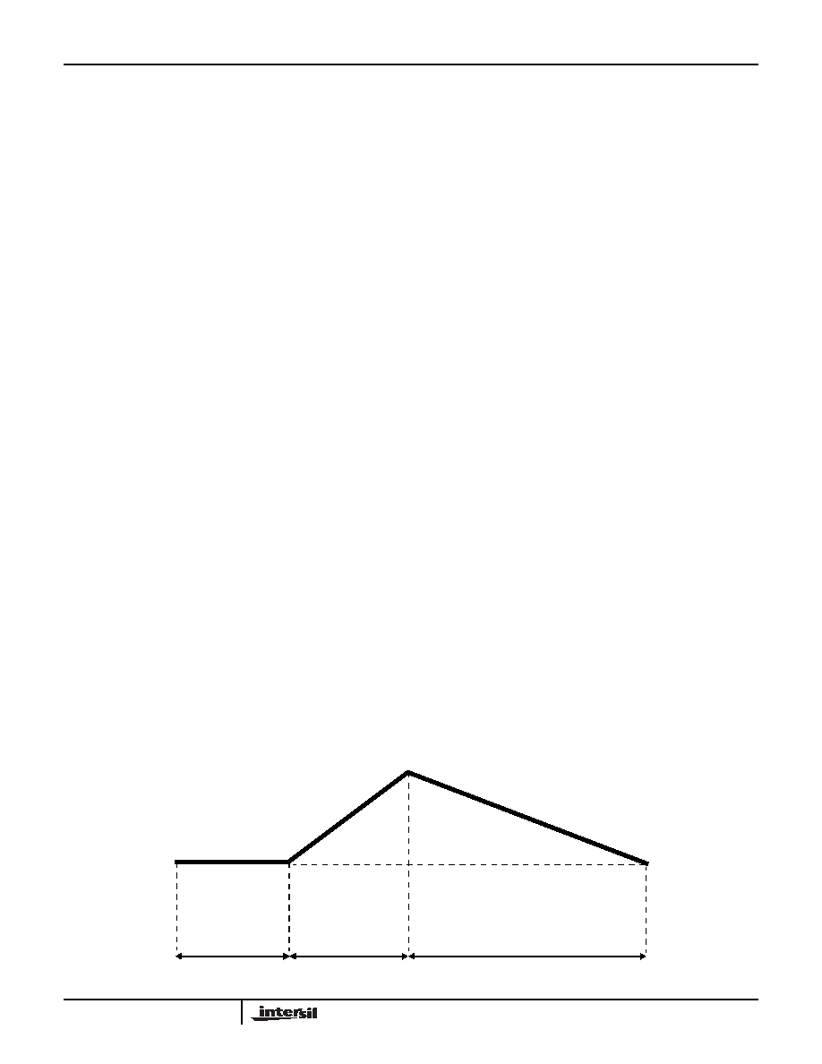
Typical Integrator Amplifier Output Waveform (INT Pin)
Design Information Summary Sheet
Ę OSCILLATOR FREQUENCY
f
OSC
= 0.45/RC
C
OSC
> 50pF; R
OSC
> 50k
f
OSC
(Typ) = 48kHz
Ę OSCILLATOR PERIOD
t
OSC
= RC/0.45
Ę INTEGRATION CLOCK FREQUENCY
f
CLOCK
= f
OSC
/4
Ę INTEGRATION PERIOD
t
INT
= 1000 x (4/f
OSC
)
Ę 60/50Hz REJECTION CRITERION
t
INT
/t
60Hz
or t
lNT
/t
60Hz
= Integer
Ę OPTIMUM INTEGRATION CURRENT
I
INT
= 4
Ą
A
Ę FULL SCALE ANALOG INPUT VOLTAGE
V
lNFS
(Typ) = 200mV or 2V
Ę INTEGRATE RESISTOR
Ę INTEGRATE CAPACITOR
Ę INTEGRATOR OUTPUT VOLTAGE SWING
Ę V
INT
MAXIMUM SWING:
(V- + 0.5V) < V
INT
< (V+ - 0.5V), V
INT
(Typ) = 2V
Ę DISPLAY COUNT
Ę CONVERSION CYCLE
t
CYC
= t
CL0CK
x 4000
t
CYC
= t
OSC
x 16,000
when f
OSC
= 48kHz; t
CYC
= 333ms
Ę COMMON MODE INPUT VOLTAGE
(V- + 1V) < V
lN
< (V+ - 0.5V)
Ę AUTO-ZERO CAPACITOR
0.01
Ą
F < C
AZ
< 1
Ą
F
Ę REFERENCE CAPACITOR
0.1
Ą
F < C
REF
< 1
Ą
F
Ę V
COM
Biased between Vi and V-.
Ę V
COM
V+ - 2.8V
Regulation lost when V+ to V- <
6.8V
If V
COM
is externally pulled down to (V+ to V-)/2,
the V
COM
circuit will turn off.
Ę ICL7106 POWER SUPPLY: SINGLE 9V
V+ - V- = 9V
Digital supply is generated internally
V
GND
V+ - 4.5V
Ę ICL7106 DISPLAY: LCD
Type: Direct drive with digital logic supply amplitude.
Ę ICL7107 POWER SUPPLY: DUAL
▒
5.0V
V+ = +5V to GND
V- = -5V to GND
Digital Logic and LED driver supply V+ to GND
Ę ICL7107 DISPLAY: LED
Type: Non-Multiplexed Common Anode
R
INT
V
INFS
I
INT
-----------------
=
C
INT
t
INT
(
)
I
INT
(
)
V
INT
--------------------------------
=
V
INT
t
INT
(
)
I
INT
(
)
C
INT
--------------------------------
=
COUNT
1000
V
IN
V
REF
---------------
ū
=
AUTO ZERO PHASE
(COUNTS)
2999 - 1000
SIGNAL INTEGRATE
PHASE FIXED
1000 COUNTS
DE-INTEGRATE PHASE
0 - 1999 COUNTS
TOTAL CONVERSION TIME = 4000 x t
CLOCK
= 16,000 x t
OSC
ICL7106, ICL7107, ICL7107S