
1
File Number
4499.1
CAUTION: These devices are sensitive to electrostatic discharge; follow proper IC Handling Procedures.
http://www.intersil.com or 407-727-9207 | Copyright ® Intersil Corporation 1999
HMP8190, HMP8191
NTSC/PAL Video Encoder
The HMP8190 and HMP8191 are NTSC and PAL encoders
designed for use in systems requiring the generation of high-
quality NTSC and PAL video.
YCbCr digital video data drive the P0-P15 inputs. The Y data
is optionally lowpass filtered to 6MHz and drives the Y
analog output. Cb and Cr are each lowpass filtered to
1.3MHz, quadrature modulated, and added together. The
result drives the C analog output. The digital Y and C data
are also added together and drive the composite analog
output.
The DACs can drive doubly-terminated (37.5
) lines, and
run at a 2x oversampling rate to simplify the analog output
filter requirements.
Applications
À DVD Players
À Video CD Players
À Digital VCRs
À Multimedia PCs
Related Products
- NTSC/PAL Encoders
- HMP8154, HMP8156A
- HMP8170 ¡ HMP8173
À NTSC/PAL Decoders
HMP8115, HMP8116
Features
À (M) NTSC and (B, D, G, H, I, M, N, NC) PAL Operation
À BT.601 and Square Pixel Operation
À Digital Input Formats
- 8-Bit, 16-Bit 4:2:2 YCbCr
- 8-Bit BT.656
À Composite and Y/C Analog Outputs
À Flexible Video Timing Control
- Timing Master or Slave
- Selectable Polarity on Each Control Signal
- Programmable Blank Output Timing
À "Sliced" VBI Data Support
- Closed Captioning
- Widescreen Signalling (WSS)
À Three 2x Oversampling, 10-Bit DACs
- Fast I
2
C Interface
Ordering Information
PART NUMBER
MACROVISION
v7.01
TEMP. RANGE (
o
C)
PACKAGE
PKG. NO.
HMP8190CN
No
0 to 70
64 Ld PQFP (Note 2)
Q64.14x14
HMP8191CN (Note 1)
Yes
0 to 70
64 Ld PQFP (Note 2)
Q64.14x14
HMP8190EVAL1 (Note 3)
Daughter Card Evaluation Platform.
NOTES:
1. The HMP8191 may be purchased by Macrovision Authorized Buyers only. This device is protected by U.S. patent numbers 4,631,603,
4,577,216, and 4,819,098, and other intellectual property rights. The use of Macrovision's copy protection technology in the device must be
authorized by Macrovision and is intended for home and other limited pay-per-view uses only, unless otherwise authorized in writing by
Macrovision. Reverse engineering or disassembly is prohibited.
2. PQFP is also known as QFP and MQFP.
3. Evaluation board descriptions are in the Applications section.
Data Sheet
May 1999
2
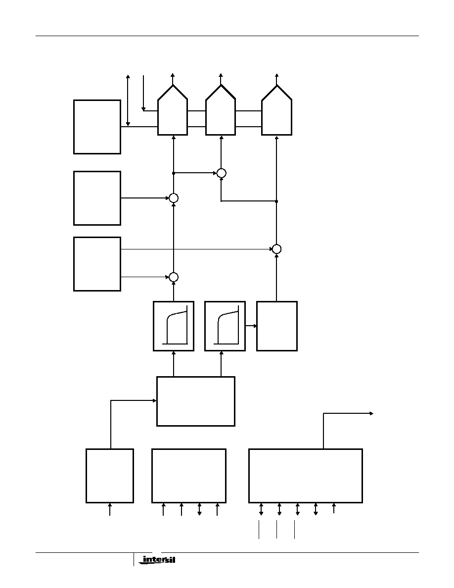
Functional Bloc
k Dia
gram
SA
SCL
SD
A
RESET
HOST
INTERF
A
C
E
P0 - P15
4:2:2 T
O
4:4:4 SAMPLE
CONVERSION
(OPTIONAL)
LP FIL
TER
Y
Cb/Cr
VBI
DA
T
A
PR
OCESSING
DAC
DAC
DAC
Y
NTSC/
C
PA
L
HSYNC
VSYNC
BLANK
CLK
VIDEO
TIMING
CLK2
FIELD
CONTR
OL
VREF
FS
ADJUST
INTERNAL
1.195V
REFERENCE
2 X
UPSAMPLE
CHR
OMA
MODULA
TION
LP FIL
TER
(4:4:4
TO
8:8:8)
MA
CR
O
VISION
PR
OCESSING
(HMP8191
ONL
Y)
+
+
+
+
HMP8190, HMP8191

3
Functional Operation
The HMP8190 and HMP8191 are fully integrated digital
encoders. Both accept YCbCr digital video input data and
generate analog video output signals. The three outputs are
one composite video signal and Y/C (S-Video).
The HMP8190/HMP8191 accepts pixel data in one of several
formats and transforms it into 4:4:4 sampled luminance and
chrominance (YCbCr) data. The encoder then interpolates the
YCbCr data to twice the pixel rate and low pass filters it to
match the bandwidth of the video output format. If enabled,
the encoder also adds vertical blanking interval (VBI)
information to the Y data. At the same time, the encoder
modulates the chrominance data with a digitally synthesized
subcarrier. Finally, the encoder outputs luminance,
chrominance, and their sum as analog signals using 10-bit
D/A converters.
The HMP8190/HMP8191 provides operating modes to
support all versions of the NTSC and PAL standards and
accepts full size input data with rectangular (BT.601) and
square pixel aspect ratios. It operates from a single clock at
twice the pixel clock rate determined by the operating mode.
The HMP8190/HMP8191's video timing control is flexible. It
may operate as the master, generating the system's video
timing control signals, or it may accept external timing
controls. The polarity of the timing controls and the number
of active pixels and lines are programmable.
Pixel Data Input
The HMP8190/HMP8191 accepts BT.601 YCbCr pixel data
via the P0-P15 input pins. The definition of each pixel input pin
is determined by the input format selected in the input format
register. The definition for each mode is shown in Table 1.
The YCbCr luminance and color difference signals are each
8 bits, scaled 0 to 255. The nominal range for Y is 16 (black)
to 235 (white). Y values less than 16 are clamped to 16;
values greater than 235 are processed normally. The
nominal range for Cb and Cr is 16 to 240 with 128
representing zero. Cb and Cr values outside their nominal
range are processed normally. Note that when converted to
the analog outputs, some combinations of YCbCr outside
their nominal ranges would generate a composite video
signal larger than the analog output limit. The composite
signal will be clipped but the S-video outputs (Y and C) will
not be.
The color difference signals are time multiplexed into one
8-bit bus beginning with a Cb sample. The Y and CbCr
busses may be input in parallel (16-bit mode) or may be time
multiplexed and input as a single bus (8-bit mode). The
single bus may also contain SAV and EAV video timing
reference codes or ancillary data (BT.656 mode).
Pixel Input and Control Signal Timing
The pixel input timing and the video control signal
input/output timing of the HMP8190/HMP8191 depend on
the part's operating mode. The periods when the encoder
samples its inputs and generates its outputs are
summarized in Table 2.
Figures 1, 2, and 3 show the timing of CLK, CLK2, BLANK,
and the pixel input data with respect to each other. BLANK
may be an input or an output; the figures show both. When it
is an input, BLANK must arrive coincident with the pixel input
data; all are sampled at the same time.
When BLANK is an output, its timing with respect to the pixel
inputs depends on the blank timing select bit in the
timing_I/O_1 register. If the bit is cleared, the
HMP8190/HMP8191 negates BLANK one CLK cycle before
it samples the pixel inputs.
If the bit is set, the encoder negates BLANK during the same
CLK cycle in which it samples the input data. In effect, the
input data must arrive one CLK cycle earlier than when the
bit is cleared. This mode is not shown in the figures.
TABLE 1. PIXEL DATA INPUT FORMATS
PIN
NAME
16-BIT
4:2:2
YCBCR
8-BIT
4:2:2
YCBCR
BT.656
P0
P1
P2
P3
P4
P5
P6
P7
Cb0, Cr0
Cb1, Cr1
Cb2, Cr2
Cb3, Cr3
Cb4, Cr4
Cb5, Cr5
Cb6, Cr6
Cb7, Cr7
Ignored
P8
P9
P10
P11
P12
P13
P14
P15
Y0
Y1
Y2
Y3
Y4
Y5
Y6
Y7
Y0, Cb0, Cr0
Y1, Cb1, Cr1
Y2, Cb2, Cr2
Y3, Cb3, Cr3
Y4, Cb4, Cr4
Y5, Cb5, Cr5
Y6, Cb6, Cr6
Y7, Cb7, Cr7
YCbCr Data,
SAV and EAV
Sequences,
and
Ancillary Data
TABLE 2. PIXEL INPUT AND CONTROL SIGNAL I/O TIMING
INPUT FORMAT
INPUT PIXEL DATA
SAMPLE
VIDEO TIMING CONTROL (NOTE 1)
CLK FREQUENCY
INPUT SAMPLE
OUTPUT ON
INPUT
OUTPUT
16-Bit YCbCr
Rising edge of CLK2 when CLK is low
Rising edge of CLK2
when CLK is high.
One-half CLK2
8-Bit YCbCr
Every rising edge of
CLK2
Every rising edge of
CLK2
Any rising edge of CLK2
Ignored
One-half CLK2
BT.656
Every rising edge of
CLK2
Not Allowed
Any rising edge of CLK2
Ignored
One-half CLK2
NOTE: Video timing control signals include HSYNC, VSYNC, BLANK and FIELD. The sync and blanking I/O directions are independent; FIELD is
always an output.
HMP8190, HMP8191

4
8-Bit YCbCr Format
When 8-bit YCbCr format is selected, the data is latched on
each rising edge of CLK2. The pixel data must be [Cb Y Cr
Y' Cb Y Cr Y' . . . ], with the first active data each scan line
being Cb data. The pixel input timing is shown in Figure 1.
As inputs, BLANK, HSYNC, and VSYNC are latched on
each rising edge of CLK2. As outputs, BLANK, HSYNC, and
VSYNC are output following the rising edge of CLK2. If the
CLK pin is configured as an input, it is ignored. If configured
as an output, it is one-half the CLK2 frequency.
16-Bit YCbCr Format
When 16-bit YCbCr format is selected, the pixel data is
latched on the rising edge of CLK2 while CLK is low. The
pixel input timing is shown in Figure 2.
As inputs, BLANK, HSYNC, and VSYNC are latched on the
rising edge of CLK2 while CLK is low. As outputs, HSYNC,
VSYNC, and BLANK are output following the rising edge of
CLK2 while CLK is high. In these modes of operation, CLK is
one-half the CLK2 frequency.
8-Bit BT.656 Format
When BT.656 format is selected, data is latched on each
rising edge of CLK2. The pixel input timing is shown in
Figure 3. The figure shows the EAV code at the end of the
line. The format of the SAV and EAV codes are shown in
Table 3.
The BT.656 input may also include ancillary data to load the
VBI or RTCI data registers. The HMP8190/HMP8191 will
use the ancillary data when enabled in the VBI data input
and timing I/O registers. The ancillary data formats and the
enable registers are described later in this datasheet.
As inputs, the BLANK, HSYNC, and VSYNC pins are
ignored since all timing is derived from the EAV and SAV
sequences within the data stream. As outputs, BLANK,
HSYNC and VSYNC are output following the rising edge of
CLK2. If the CLK pin is configured as an input, it is ignored. If
configured as an output, it is one-half the CLK2 frequency.
FIGURE 1. PIXEL INPUT TIMING - 8-BIT YCBCR
FIGURE 2. PIXEL INPUT TIMING - 16-BIT YCBCR
Cb 0
Y 0
Cr 0
Y 1
Cb 2
Y 2
CLK2
P8-P15
BLANK
(INPUT)
Y N
BLANK
(OUTPUT)
Y 0
Y 1
Y 2
Y 3
Y 4
Y 5
CLK
P8-P15
BLANK
(INPUT)
Cb 0
Cr 0
Cb 2
Cr 2
Cb 4
Cr 4
P0-P7
CLK2
Y N
Cr N-1
BLANK
(OUTPUT)
HMP8190, HMP8191

5
Video Timing Control
The pixel input data and the output video timing of the
HMP8190/HMP8191 are at 50 or 59.94 fields per second
interlaced. The timing is controlled by the BLANK, HSYNC,
VSYNC, FIELD, and CLK2 pins.
HSYNC, VSYNC, and Field Timing
The leading edge of HSYNC indicates the beginning of a
horizontal sync interval. If HSYNC is an output, it is asserted
for about 4.7
Á
s. If HSYNC is an input, it must be active for at
least two CLK2 periods. The width of the analog horizontal
sync tip is determined from the video standard and does not
depend on the width of HSYNC.
The leading edge of VSYNC indicates the beginning of a
vertical sync interval. If VSYNC is an output, it is asserted for
3 scan lines in (MM) NTSC and (M, N) PAL modes or 2.5
scan lines in (B, D, G, H, I, NC) PAL modes. If VSYNC is an
input, it must be asserted for at least two CLK2 periods.
When HSYNC and VSYNC are configured as outputs, their
leading edges will occur simultaneously at the start of an
odd field. At the start of an even field, the leading edge of
VSYNC occurs in the middle of the line.
When HSYNC and VSYNC are configured as inputs, the
HMP8190/HMP8191 provides a programmable HSYNC
window for determining FIELD. The window is specified with
respect to the leading or trailing edge of VSYNC. The edge
is selected in the field control register. When HSYNC is
found inside the window, then the encoder sets FIELD to the
value specified in the field control register.
The HMP8190/HMP8191 provides programmable timing for
the VSYNC input. At the active edge of VSYNC, the encoder
resets its vertical half-line counter to the value specified by
the field control register. This allows the input and output
syncs to be offset, although the data must still be aligned.
The FIELD signal is always an output and changes state
near each leading edge of VSYNC. The delay between the
syncs and FIELD depends on the encoder's operating mode
as summarized in Table 4. In modes in which the encoder
uses CLK to gate its inputs and outputs, the FIELD signal
may be delayed 0-12 additional CLK2 periods.
Figure 4 illustrates the HSYNC, VSYNC, and FIELD general
timing for (M) NTSC and (M, N) PAL. Figure 5 illustrates the
general timing for (B, D, G, H, I, NC) PAL. In the figures, all
the signals are shown active low (their reset state), and
FIELD is low during odd fields.
FIGURE 3. PIXEL INPUT TIMING - BT.656
TABLE 3. BT.656 EAV AND SAV SEQUENCES
PIXEL INPUT
P15
P14
P13
P12
P11
P10
P9
P8
Preamble Word 1
1
1
1
1
1
1
1
1
Preamble Word 2
0
0
0
0
0
0
0
0
Preamble Word 3
0
0
0
0
0
0
0
0
Status Word
1
F
V
H
P3
P2
P1
P0
NOTE:
F: 0 = Field 1; 1 = Field 2
V: 0 = Active Line; 1 = Vertical Blanking
H: 0 = Start Active Video; 1 = End Active Video
P3 - P0: Protection bits; Ignored
Cb 2
Y 2
Cr 2
Y 3
Cb 4
Y 4
CLK2
P8-P15
"FF"
"00"
BLANK
(OUTPUT)
"00"
EAV
"10"
"10"
"80"
TABLE 4. FIELD OUTPUT TIMING
OPERATING MODE
CLK2
DELAY
COMMENTS
SYNC I/O
DIRECTION
BLANK I/O
DIRECTION
Input
Input
148
FIELD lags VSYNC switch-
ing from odd to even.
FIELD lags the earlier of
VSYNC and HSYNC when
syncs are aligned when
switching from even to odd.
Input
Output
138
FIELD lags VSYNC.
Output
Don't Care
32
FIELD leads VSYNC.
HMP8190, HMP8191