Other brands and names are the property of their respective owners
Information in this document is provided in connection with Intel products Intel assumes no liability whatsoever including infringement of any patent or
copyright for sale and use of Intel products except as provided in Intel's Terms and Conditions of Sale for such products Intel retains the right to make
changes to these specifications at any time without notice Microcomputer Products may have minor variations to this specification known as errata
December 1995
COPYRIGHT
INTEL CORPORATION 1996
Order Number 290414-003
UPI-C42 UPI-L42
UNIVERSAL PERIPHERAL INTERFACE
CHMOS 8-BIT SLAVE MICROCONTROLLER
Y
Pin Software and Architecturally
Compatible with all UPI-41 and UPI-42
Products
Y
Low Voltage Operation with the UPI-
L42
Full 3 3V Support
Y
Hardware A20 Gate Support
Y
Suspend Power Down Mode
Y
Security Bit Code Protection Support
Y
8-Bit CPU plus ROM OTP EPROM RAM
I O Timer Counter and Clock in a
Single Package
Y
4096 x 8 ROM OTP 256 x 8 RAM 8-Bit
Timer Counter 18 Programmable I O
Pins
Y
DMA Interrupt or Polled Operation
Supported
Y
One 8-Bit Status and Two Data
Registers for Asynchronous Slave-to-
Master Interface
Y
Fully Compatible with all Intel and Most
Other Microprocessor Families
Y
Interchangeable ROM and OTP EPROM
Versions
Y
Expandable I O
Y
Sync Mode Available
Y
Over 90 Instructions 70% Single Byte
Y
Quick Pulse Programming Algorithm
Fast OTP Programming
Y
Available in 40-Lead Plastic 44-Lead
Plastic Leaded Chip Carrier and
44-Lead Quad Flat Pack Packages
(See Packaging Spec Order
240800 Package Type P N
and S)
The UPI-C42 is an enhanced CHMOS version of the industry standard Intel UPI-42 family It is fabricated on
Intel's CHMOS III-E process The UPI-C42 is pin software and architecturally compatible with the NMOS UPI
family The UPI-C42 has all of the same features of the NMOS family plus a larger user programmable memory
array (4K) hardware A20 gate support and lower power consumption inherent to a CHMOS product
The UPI-L42 offers the same functionality and socket compatibility as the UPI-C42 as well as providing low
voltage 3 3V operation
The UPI-C42 is essentially a ``slave'' microcontroller or a microcontroller with a slave interface included on the
chip Interface registers are included to enable the UPI device to function as a slave peripheral controller in the
MCS Modules and iAPX family as well as other 8- 16- and 32-bit systems
To allow full user flexibility the program memory is available in ROM and One-Time Programmable EPROM
(OTP)
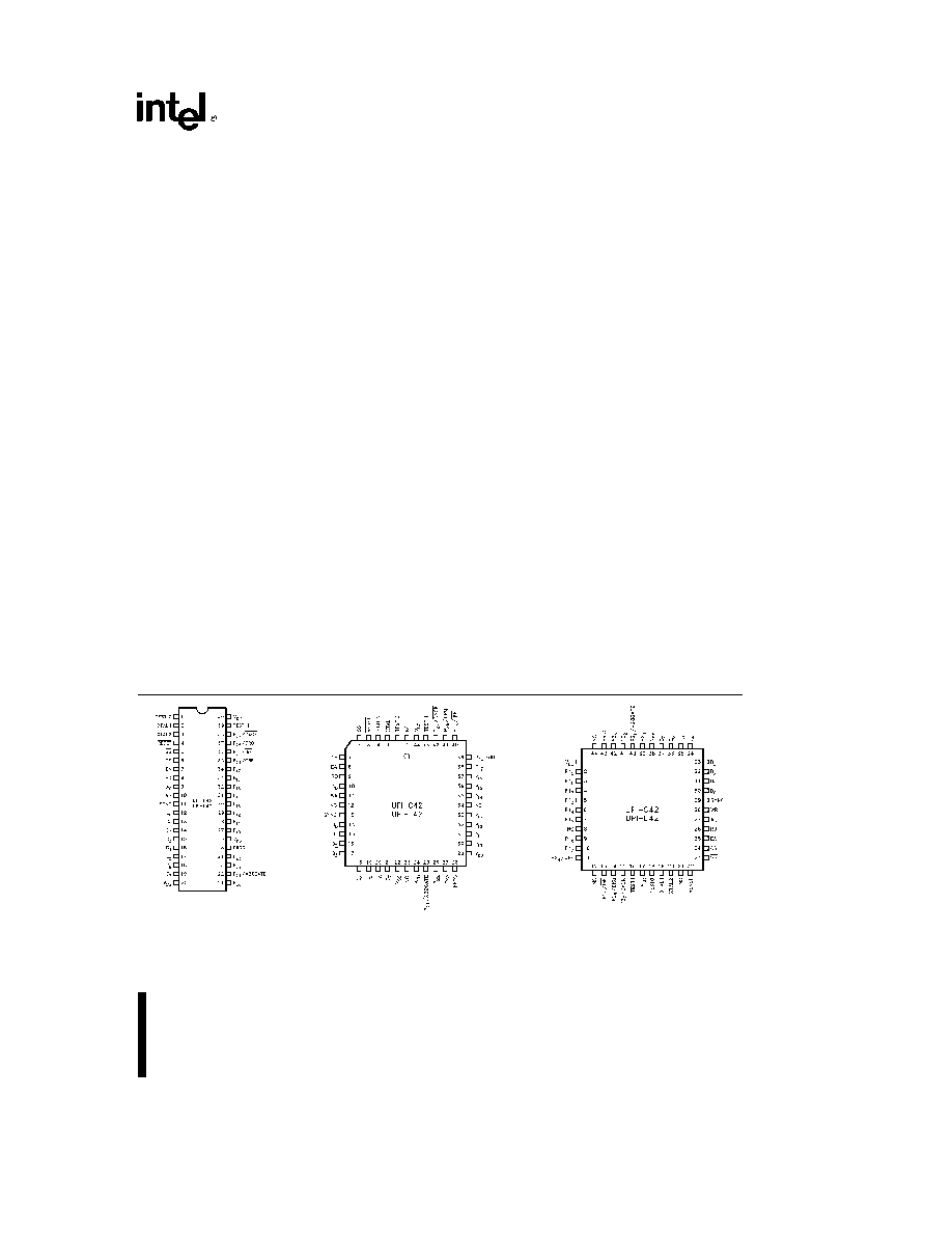
290414 ş 1
Figure 1 DIP Pin
Configuration
290414 ş 2
Figure 2 PLCC Pin Configuration
290414 ş 3
Figure 3 QFP Pin Configuration
UPI-C42 UPI-L42
Table 1 Pin Description
DIP
PLCC
QFP
Symbol
Pin
Pin
Pin
Type
Name and Function
No
No
No
TEST 0
1
2
18
I
TEST INPUTS
Input pins which can be directly tested using conditional
branch instructions
TEST 1
39
43
16
FREQUENCY REFERENCE
TEST 1 (T
1
) functions as the event timer
input (under software control) TEST 0 (T
0
) is a multi-function pin used
during PROM programming and ROM EPROM verification during Sync
Mode to reset the instruction state to S1 and synchronize the internal clock
to PH1
XTAL 1
2
3
19
O
OUTPUT
Output from the oscillator amplifier
XTAL 2
3
4
20
I
INPUT
Input to the oscillator amplifier and internal clock generator
circuits
RESET
4
5
22
I
RESET
Input used to reset status flip-flops set the program counter to
zero and force the UPI-C42 from the suspend power down mode
RESET is also used during EPROM programming and verification
SS
5
6
23
I
SINGLE STEP
Single step input used in conjunction with the SYNC output
to step the program through each instruction (EPROM) This should be tied
to
a
5V when not used This pin is also used to put the device in Sync
Mode by applying 12 5V to it
CS
6
7
24
I
CHIP SELECT
Chip select input used to select one UPI microcomputer
out of several connected to a common data bus
EA
7
8
25
I
EXTERNAL ACCESS
External access input which allows emulation
testing and ROM EPROM verification This pin should be tied low if
unused
RD
8
9
26
I
READ
I O read input which enables the master CPU to read data and
status words from the OUTPUT DATA BUS BUFFER or status register
A
0
9
10
27
I
COMMAND DATA SELECT
Address Input used by the master processor
to indicate whether byte transfer is data (A
0
e
0 F1 is reset) or command
(A
0
e
1 F1 is set) A
0
e
0 during program and verify operations
WR
10
11
28
I
WRITE
I O write input which enables the master CPU to write data and
command words to the UPI INPUT DATA BUS BUFFER
SYNC
11
13
29
O
OUTPUT CLOCK
Output signal which occurs once per UPI instruction
cycle SYNC can be used as a strobe for external circuitry it is also used to
synchronize single step operation
D
0
ş D
7
(BUS)
12 ş 19
14 ş 21
30 ş 37
I O
DATA BUS
Three-state bidirectional DATA BUS BUFFER lines used to
interface the UPI microcomputer to an 8-bit master system data bus
P
10
ş P
17
27 ş 34
30 ş 33
2 ş 10
I O
PORT 1
8-bit PORT 1 quasi-bidirectional I O lines P
10
ş P
17
access the
signature row and security bit
35 ş 38
2
UPI-C42 UPI-L42
Table 1 Pin Description
(Continued)
DIP
PLCC
QFP
Symbol
Pin
Pin
Pin
Type
Name and Function
No
No
No
P
20
ş P
27
21 ş 24
24 ş 27
39 ş 42
I O
PORT 2
8-bit PORT 2 quasi-bidirectional I O lines The lower 4 bits
(P
20
ş P
23
) interface directly to the 8243 I O expander device and
35 ş 38
39 ş 42
11 13 ş 15
contain address and data information during PORT 4 ş 7 access P
21
can be programmed to provide hardware A20 gate support The upper
4 bits (P
24
ş P
27
) can be programmed to provide interrupt Request and
DMA Handshake capability Software control can configure P
24
as
Output Buffer Full (OBF) interrupt P
25
as Input Buffer Full (IBF)
interrupt P
26
as DMA Request (DRQ) and P
27
as DMA ACKnowledge
(DACK)
PROG
25
28
43
I O
PROGRAM
Multifunction pin used as the program pulse input during
PROM programming
During I O expander access the PROG pin acts as an address data
strobe to the 8243 This pin should be tied high if unused
V
CC
40
44
17
POWER
a
5V main power supply pin
V
DD
26
29
1
POWER
a
5V during normal operation
a
12 75V during programming
operation Low power standby supply pin
V
SS
20
22
38
GROUND
Circuit ground potential
290414 ş 4
Figure 4 Block Diagram
3
UPI-C42 UPI-L42
UPI-C42 L42 PRODUCT SELECTION GUIDE
UPI-C42
Low power CHMOS version of the UPI-42
Device
Package
ROM
OTP
Comments
80C42
N P S
4K
ROM Device
82C42PC
N P S
Phoenix MultiKey 42 firmware PS 2 style mouse support
82C42PD
N P S
Phoenix MultiKey 42L firmware KBC and SCC for portable apps
82C42PE
N P S
Phoenix MultiKey 42G firmware Energy Efficient KBC solution
87C42
N P S
4K
One Time Programmable Version
UPI-L42
The low voltage 3 3V version of the UPI-C42
Device
Package
ROM
OTP
Comments
80L42
N P S
4K
ROM Device
82L42PC
N P S
Phoenix MultiKey 42 firmware PS 2 style mouse support
82L42PD
N P S
Phoenix MultiKey 42L firmware KBC and SCC for portable apps
87L42
N P S
4K
One Time Programmable Version
N
e
44 lead PLCC P
e
40 lead PDIP S
e
44 lead QFP D
e
40 lead CERDIP
KBC
e
Key Board Control SCC
e
Scan Code Control
THE INTEL 82C42
As shown in the UPI-C42 product matrix the UPI-
C42 is offered as a pre-programmed 80C42 with var-
ious versions of MultiKey 42 keyboard controller
firmware developed by Phoenix Technologies Ltd
The 82C42PC provides a low powered solution for
industry standard keyboard and PS 2 style mouse
control The 82C42PD provides a cost effective
means for keyboard and scan code control for note-
book platforms The 82C42PE allows a quick time to
market low cost solution for energy efficient desk-
top designs
4
UPI-C42 UPI-L42
UPI-42 COMPATIBLE FEATURES
1
Two Data Bus Buffers one for input and one for
output This allows a much cleaner Master Slave
protocol
290414 ş 5
2
8 Bits of Status
ST
7
ST
6
ST
5
ST
4
F
1
F
0
IBF OBF
D
7
D
6
D
5
D
4
D
3
D
2
D
1
D
0
ST
4
ş ST
7
are user definable status bits These
bits are defined by the ``MOV STS A'' single
byte single cycle instruction Bits 4 ş 7 of the
acccumulator are moved to bits 4 ş 7 of the status
register Bits 0 ş 3 of the status register are not
affected
MOV STS A
Op Code 90H
1
0
0
1
0
0
0
0
D
7
D
0
3
RD and WR are edge triggered IBF OBF F
1
and
INT change internally after the trailing edge of RD
or WR
During the time that the host CPU is reading the
status register the UPI is prevented from updat-
ing this register or is `locked out '
290414 ş 6
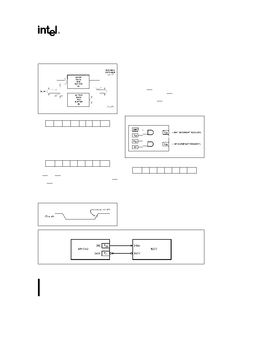
4
P
24
and P
25
are port pins or Buffer Flag pins
which can be used to interrupt a master proces-
sor These pins default to port pins on Reset
If the ``EN FLAGS'' instruction has been execut-
ed P
24
becomes the OBF (Output Buffer Full)
pin A ``1'' written to P
24
enables the OBF pin (the
pin outputs the OBF Status Bit) A ``0'' written to
P
24
disables the OBF pin (the pin remains low)
This pin can be used to indicate that valid data is
available from the UPI (in Output Data Bus Buff-
er)
If ``EN FLAGS'' has been executed P
25
be-
comes the IBF (Input Buffer Full) pin A ``1'' writ-
ten to P
25
enables the IBF pin (the pin outputs
the inverse of the IBF Status Bit A ``0'' written to
P
25
disables the IBF pin (the pin remains low)
This pin can be used to indicate that the UPI is
ready for data
Data Bus Buffer Interrupt Capability
290414 ş 7
EN FLAGS
Op Code 0F5H
1
1
1
1
0
1
0
1
D
7
D
0
5
P
26
and P
27
are port pins or DMA handshake
pins for use with a DMA controller These pins
default to port pins on Reset
If the ``EN DMA'' instruction has been executed
P
26
becomes the DRQ (DMA Request) pin A ``1''
written to P
26
causes a DMA request (DRQ is
activated) DRQ is deactivated by DACK
RD
DACK
WR or execution of the ``EN DMA'' in-
struction
DMA Handshake Capability
290414 ş 8
5