Äîêóìåíòàöèÿ è îïèñàíèÿ www.docs.chipfind.ru

Intel® PXA255 Processor
Electrical, Mechanical, and Thermal Specification
Data Sheet
Product Features
High Performance Processor
--Intel® XScaleTM Microarchitecture
--32 KB Instruction Cache
--32 KB Data Cache
--2 KB "mini" Data Cache
--Extensive Data Buffering
Intel® Media Processing Technology
--Enhanced 16-bit Multiply
--40-bit Accumulator
Flexible Clocking
--CPU clock from 100 to 400 MHz
--Flexible memory clock ratios
--Frequency change modes
Rich Serial Peripheral Set
--AC97 Audio Port
--I
2
S Audio Port
--USB Client Controller
--High Speed UART
--Second UART with flow control
--UART with hardware flow control
--FIR and SIR infrared comm ports
Low Power
--Less than 500 mW Typical Internal
Dissipation
--Supply Voltage may be Reduced to
1.00 V
--Low Power/Sleep Modes
High Performance Memory Controller
--Four Banks of SDRAM - up to 100 MHz
--Five Static Chip Selects
--Support for PCMCIA or Compact Flash
--Companion Chip interface
Additional Peripherals for system
connectivity
--Multimedia Card Controller (MMC)
--SSP Controller
--Network SSP controller for baseband
--I2C Controller
--Two Pulse Width Modulators (PWMs)
--All peripheral pins double as GPIOs
Hardware debug features
Hardware Performance Monitoring features
Order Number: 278805-002
February, 2004

2
Data Sheet
INFORMATION IN THIS DOCUMENT IS PROVIDED IN CONNECTION WITH INTEL® PRODUCTS. NO LICENSE, EXPRESS OR IMPLIED, BY
ESTOPPEL OR OTHERWISE, TO ANY INTELLECTUAL PROPERTY RIGHTS IS GRANTED BY THIS DOCUMENT. EXCEPT AS PROVIDED IN
INTEL'S TERMS AND CONDITIONS OF SALE FOR SUCH PRODUCTS, INTEL ASSUMES NO LIABILITY WHATSOEVER, AND INTEL DISCLAIMS
ANY EXPRESS OR IMPLIED WARRANTY, RELATING TO SALE AND/OR USE OF INTEL PRODUCTS INCLUDING LIABILITY OR WARRANTIES
RELATING TO FITNESS FOR A PARTICULAR PURPOSE, MERCHANTABILITY, OR INFRINGEMENT OF ANY PATENT, COPYRIGHT OR OTHER
INTELLECTUAL PROPERTY RIGHT. Intel products are not intended for use in medical, life saving, or life sustaining applications.
Intel may make changes to specifications and product descriptions at any time, without notice.
Designers must not rely on the absence or characteristics of any features or instructions marked "reserved" or "undefined." Intel reserves these for
future definition and shall have no responsibility whatsoever for conflicts or incompatibilities arising from future changes to them.
The PXA255 processor EMTS Data Sheet may contain design defects or errors known as errata which may cause the product to deviate from
published specifications. Current characterized errata are available on request.
MPEG is an international standard for video compression/decompression promoted by ISO. Implementations of MPEG CODECs, or MPEG enabled
platforms may require licenses from various entities, including Intel Corporation.
Contact your local Intel sales office or your distributor to obtain the latest specifications and before placing your product order.
Copies of documents which have an ordering number and are referenced in this document, or other Intel literature may be obtained by calling
1-800-548-4725 or by visiting Intel's website at http://www.intel.com.
Copyright © Intel Corporation, 2004
*Other names and brands may be claimed as the property of others.

PXA255 Processor -- Electrical, Mechanical, and Thermal Specification
Data Sheet
3
Contents
1.0
About This Document ............................................................................................7
2.0
Functional Overview ..............................................................................................7
3.0
Package Information ..............................................................................................8
3.1
Package Introduction.....................................................................................8
3.1.1
Functional Signal Definitions ............................................................8
3.1.1.1
PXA255 Processor Signal Pin Descriptions .....................8
3.2
Package Power Ratings ..............................................................................22
4.0
Electrical Specifications ......................................................................................22
4.1
Absolute Maximum Ratings.........................................................................22
4.2
Power Consumption Specifications .............................................................23
4.3
Operating Conditions...................................................................................25
4.4
Targeted DC Specifications.........................................................................26
4.5
Targeted AC Specifications .........................................................................27
4.6
Oscillator Electrical Specifications...............................................................28
4.6.1
32.768-kHz Oscillator Specifications ..............................................28
4.6.2
3.6864 MHz Oscillator Specifications .............................................29
4.7
Reset and Power AC Timing Specifications ................................................30
4.7.1
Power-On Timing ...........................................................................30
4.7.2
Hardware Reset Timing..................................................................32
4.7.3
Watchdog Reset Timing .................................................................32
4.7.4
GPIO Reset Timing ........................................................................32
4.7.5
Sleep Mode Timing ........................................................................33
4.8
Memory Bus and PCMCIA AC Specifications .............................................35
4.9
Peripheral Module AC Specifications ..........................................................37
4.9.1
LCD Module AC Timing..................................................................37
4.9.2
SSP Module AC Timing..................................................................37
4.9.3
Boundary Scan Test Signal Timings ..............................................38
4.10 AC Test Conditions .....................................................................................39

PXA255 Processor -- Electrical, Mechanical, and Thermal Specification
4
Data Sheet
Figures
1
Processor Block Diagram...................................................................................... 8
2
PXA255 processor .............................................................................................. 19
3
Power-On Reset Timing ...................................................................................... 31
4
Hardware Reset Timing ...................................................................................... 32
5
GPIO Reset Timing ............................................................................................. 33
6
Sleep Mode Timing ............................................................................................. 34
7
LCD AC Timing Definitions ................................................................................. 37
8
SSP AC Timing Definitions ................................................................................. 38
9
AC Test Load ...................................................................................................... 39
Tables
1
Related Documentation......................................................................................... 7
2
Processor Pin Types ............................................................................................. 9
3
Pin and Signal Descriptions for the PXA255 Processor........................................ 9
4
Pin Description Notes.......................................................................................... 18
5
PXA255 processor 256-Lead 17x17mm mBGA Pinout -- Ballpad No. Order .... 20
6
JA
and Maximum Power Ratings........................................................................ 22
7
Absolute Maximum Ratings ................................................................................ 23
8
Power Consumption Specifications for PXA255 processor ................................ 24
9
Voltage, Temperature, and Frequency Electrical Specifications......................... 25
10 Standard Input, Output, and I/O Pin DC Operating Conditions ........................... 26
11 Standard Input, Output, I/O Pin DC Operating Conditions for 2.5-V Memory ..... 27
12 Standard Input, Output, and I/O Pin AC Operating Conditions ........................... 28
13 32.768-kHz Oscillator Specifications................................................................... 28
14 3.6864-MHz Oscillator Specifications ................................................................. 29
15 Power-On Timing Specifications ......................................................................... 31
16 Hardware Reset Timing Specifications ............................................................... 32
17 GPIO Reset Timing Specifications ...................................................................... 33
18 Sleep Mode Timing Specifications ...................................................................... 34
19 SRAM / ROM / Flash / Synchronous Fast Flash AC Specifications.................... 35
20 Variable Latency I/O Interface AC Specifications ............................................... 35
21 Card Interface (PCMCIA or Compact Flash) AC Specifications ......................... 36
22 Synchronous Memory Interface AC Specifications 1 .......................................... 36
23 LCD AC Timing Specifications ............................................................................ 37
24 SSP AC Timing Specifications ............................................................................ 38
25 Boundary Scan Test Signal Timing ..................................................................... 38
PXA255 Processor -- Electrical, Mechanical, and Thermal Specification
Data Sheet
5
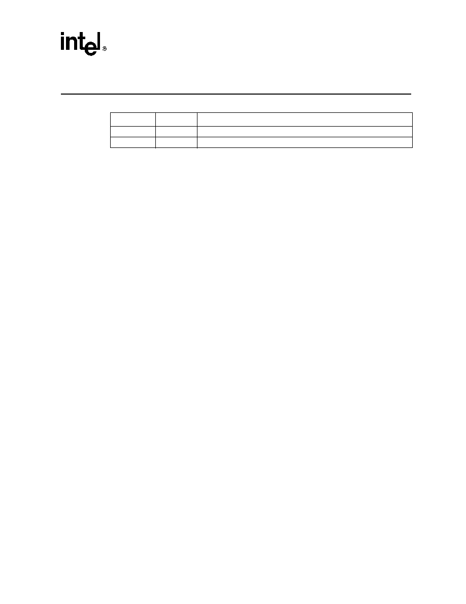
Revision History
Date
Revision
Description
March 2003
-001
First public release of the EMTS
February 2004
-002
Updated 400 MHz Idle mode power.
Document Outline