
Intel
ģ
E7501 Chipset Memory
Controller Hub (MCH)
Datasheet
December 2002
Document Number: 251927-001

2
Intel
ģ
E7501 Chipset MCH Datasheet
INFORMATION IN THIS DOCUMENT IS PROVIDED IN CONNECTION WITH INTEL
ģ
PRODUCTS. NO LICENSE, EXPRESS OR IMPLIED, BY
ESTOPPEL OR OTHERWISE, TO ANY INTELLECTUAL PROPERTY RIGHTS IS GRANTED BY THIS DOCUMENT. EXCEPT AS PROVIDED IN
INTEL'S TERMS AND CONDITIONS OF SALE FOR SUCH PRODUCTS, INTEL ASSUMES NO LIABILITY WHATSOEVER, AND INTEL DISCLAIMS
ANY EXPRESS OR IMPLIED WARRANTY, RELATING TO SALE AND/OR USE OF INTEL PRODUCTS INCLUDING LIABILITY OR WARRANTIES
RELATING TO FITNESS FOR A PARTICULAR PURPOSE, MERCHANTABILITY, OR INFRINGEMENT OF ANY PATENT, COPYRIGHT OR OTHER
INTELLECTUAL PROPERTY RIGHT. Intel products are not intended for use in medical, life saving, or life sustaining applications.
Intel may make changes to specifications and product descriptions at any time, without notice.
Designers must not rely on the absence or characteristics of any features or instructions marked "reserved" or "undefined." Intel reserves these for
future definition and shall have no responsibility whatsoever for conflicts or incompatibilities arising from future changes to them.
The Intel
ģ
E7501 chipset MCH component may contain design defects or errors known as errata which may cause the product to deviate from
published specifications. Current characterized errata are available on request.
Contact your local Intel sales office or your distributor to obtain the latest specifications and before placing your product order.
Intel, Intel Xeon, and the Intel logo are trademarks or registered trademarks of Intel corporation or its subsidiaries in the United States and other
countries.
*Other names and brands may be claimed as the property of others.
Copyright © 2002, Intel Corporation

Intel
ģ
E7501 Chipset MCH Datasheet
3
Contents
1
Introduction
................................................................................................................13
1.1
Terminology.........................................................................................................13
1.2
Reference Documents.........................................................................................14
1.3
Intel
ģ
E7501 Chipset System Architecture..........................................................14
2
Signal Description
...................................................................................................17
2.1
System Bus Interface Signals .............................................................................19
2.2
DDR Channel A Signals ......................................................................................22
2.3
DDR Channel B Signals ......................................................................................23
2.4
Hub Interface_A Signals......................................................................................24
2.5
Hub Interface_B Signals......................................................................................25
2.6
Hub Interface_C Signals .....................................................................................26
2.7
Hub Interface_D Signals .....................................................................................27
2.8
Clocks, Reset, Power, and Miscellaneous Signals .............................................28
3
Register Description
...............................................................................................29
3.1
Register Terminology ..........................................................................................29
3.2
Platform Configuration.........................................................................................30
3.2.1
Standard PCI Configuration Mechanism ................................................31
3.3
PCI Configuration Cycle Routing.........................................................................31
3.3.1
Logical PCI Bus 0 Configuration Mechanism .........................................32
3.3.2
Primary PCI Downstream Configuration Mechanism .............................32
3.3.3
HI_B, HI_C, HI_D Bus Configuration Mechanism ..................................32
3.4
I/O Mapped Registers .........................................................................................33
3.4.1
CONFIG_ADDRESS--Configuration Address Register ........................33
3.4.2
CONFIG_DATA--Configuration Data Register......................................33
3.5
Chipset Host Controller Registers (Device 0, Function 0)...................................34
3.5.1
VID--Vendor Identification Register (D0:F0) .........................................35
3.5.2
DID--Device Identification Register (D0:F0)..........................................35
3.5.3
PCICMD--PCI Command Register (D0:F0) ..........................................36
3.5.4
PCISTS--PCI Status Register (D0:F0) ..................................................37
3.5.5
RID--Revision Identification Register (D0:F0) .......................................38
3.5.6
SUBC--Sub-Class Code Register (D0:F0) ............................................38
3.5.7
BCC--Base Class Code Register (D0:F0).............................................38
3.5.8
MLT--Master Latency Timer Register (D0:F0) ......................................39
3.5.9
HDR--Header Type Register (D0:F0)....................................................39
3.5.10 SVID--Subsystem Vendor Identification Register (D0:F0) ....................39
3.5.11 SID--Subsystem Identification Register (D0:F0) ...................................40
3.5.12 CAPPTR--Capabilities Pointer Register (D0:F0)...................................40
3.5.13 MCHCAP--MCH Capabilities Structure Register (D0:F0) .....................41
3.5.14 MCHCFG--MCH Configuration Register (D0:F0)..................................41
3.5.15 MCHCFGNS--MCH Configuration Register (D0:F0).............................43
3.5.16 FDHC--Fixed DRAM Hole Control Register (D0:F0).............................43
3.5.17 PAM[6:0]--Programmable Attribute Map Registers (D0:F0)..................44
3.5.18 DRB[0:7]--DRAM Row Boundary Register (D0:F0) ..............................46
3.5.19 DRA[3:0]--DRAM Row Attribute Register (D0:F0) ................................47

4
Intel
ģ
E7501 Chipset MCH Datasheet
3.5.20 DRT--DRAM Timing Register (D0:F0) .................................................. 48
3.5.21 DRC--DRAM Controller Mode Register (D0:F0) ................................... 50
3.5.22 CKDIS--CK / CK# Disable Register (D0:F0) ......................................... 51
3.5.23 CFGCTL--Configuration Control Register (D0:F0)................................ 52
3.5.24 SMRAMC--System Management RAM Control Register (D0:F0)......... 53
3.5.25 ESMRAMC--Extended System Management RAM Control
Register (D0:F0)..................................................................................... 54
3.5.26 TOLM--Top of Low Memory Register (D0:F0) ...................................... 55
3.5.27 REMAPBASE--Remap Base Address Register (D0:F0)....................... 55
3.5.28 REMAPLIMIT--Remap Limit Address Register (D0:F0)........................ 56
3.5.29 SKPD--Scratchpad Data Register (D0:F0)............................................ 56
3.5.30 DVNP--Device Not Present Register (D0:F0) ....................................... 57
3.6
Host RASUM Controller Registers (Device 0, Function 1).................................. 58
3.6.1
VID--Vendor Identification Register (D0:F1) ......................................... 59
3.6.2
DID--Device Identification Register (D0:F1).......................................... 59
3.6.3
PCICMD--PCI Command Register (D0:F1) .......................................... 60
3.6.4
PCISTS--PCI Status Register (D0:F1).................................................. 61
3.6.5
RID--Revision Identification Register (D0:F1) ....................................... 61
3.6.6
SUBC--Sub-Class Code Register (D0:F1) ............................................ 62
3.6.7
BCC--Base Class Code Register (D0:F1)............................................. 62
3.6.8
MLT--Master Latency Timer Register (D0:F1) ...................................... 62
3.6.9
HDR--Header Type Register (D0:F1).................................................... 63
3.6.10 SVID--Subsystem Vendor Identification Register (D0:F1) .................... 63
3.6.11 SID--Subsystem Identification Register (D0:F1) ................................... 63
3.6.12 FERR_GLOBAL--First Global Error Register (D0:F1)........................... 64
3.6.13 NERR_GLOBAL--Next Global Error Register (D0:F1).......................... 65
3.6.14 HIA_FERR--HI_A First Error Register (D0:F1) ..................................... 66
3.6.15 HIA_NERR--HI_A Next Error Register (D0:F1)..................................... 67
3.6.16 SCICMD_HIA--SCI Command Register (D0:F1) .................................. 68
3.6.17 SMICMD_HIA--SMI Command Register (D0:F1).................................. 69
3.6.18 SERRCMD_HIA--SERR Command Register (D0:F1) .......................... 70
3.6.19 SYSBUS_FERR--System Bus First Error Register (D0:F1).................. 71
3.6.20 SYSBUS_NERR-- System Bus Next Error Register (D0:F1)................ 72
3.6.21 SCICMD_SYSBUS--SCI Command Register (D0:F1).......................... 73
3.6.22 SMICMD_SYSBUS--SMI Command Register (D0:F1) ......................... 74
3.6.23 SERRCMD_SYSBUS--SERR Command Register (D0:F1).................. 75
3.6.24 DRAM_FERR--DRAM First Error Register (D0:F1) .............................. 76
3.6.25 DRAM_NERR--DRAM Next Error Register (D0:F1) ............................. 76
3.6.26 SCICMD_DRAM--SCI Command Register (D0:F1).............................. 77
3.6.27 SMICMD_DRAM--SMI Command Register (D0:F1) ............................. 77
3.6.28 SERRCMD_DRAM--SERR Command Register (D0:F1)...................... 78
3.6.29 DRAM_CELOG_ADD--DRAM First Correctable Memory Error
Address Register (D0:F1)....................................................................... 78
3.6.30 DRAM_UELOG_ADD--DRAM First Uncorrectable Memory Error
Address Register (D0:F1)....................................................................... 79
3.6.31 DRAM_CELOG_SYNDROME--DRAM First Correctable Memory
Error Syndrome Register (D0:F1) .......................................................... 79
3.7
Hub Interface_B PCI-to-PCI Bridge Registers (Device 2, Function 0) ................ 80
3.7.1
VID--Vendor Identification Register (D2:F0) ......................................... 81
3.7.2
DID--Device Identification Register (D2:F0).......................................... 81

Intel
ģ
E7501 Chipset MCH Datasheet
5
3.7.3
PCICMD--PCI Command Register (D2:F0) ..........................................82
3.7.4
PCISTS--PCI Status Register (D2:F0) ..................................................83
3.7.5
RID--Revision Identification Register (D2:F0) .......................................84
3.7.6
SUBC--Sub-Class Code Register (D2:F0) ............................................84
3.7.7
BCC--Base Class Code Register (D2:F0).............................................84
3.7.8
MLT--Master Latency Timer Register (D2:F0) ......................................85
3.7.9
HDR--Header Type Register (D2:F0)....................................................85
3.7.10 PBUSN--Primary Bus Number Register (D2:F0) ..................................86
3.7.11 SBUSN--Secondary Bus Number Register (D2:F0)..............................86
3.7.12 SUBUSN--Subordinate Bus Number Register (D2:F0).........................87
3.7.13 SMLT--Secondary Bus Master Latency Timer Register (D2:F0) ..........87
3.7.14 IOBASE--I/O Base Address Register (D2:F0).......................................88
3.7.15 IOLIMIT--I/O Limit Address Register (D2:F0)........................................88
3.7.16 SEC_STS--Secondary Status Register (D2:F0) ...................................89
3.7.17 MBASE--Memory Base Address Register (D2:F0) ...............................90
3.7.18 MLIMIT--Memory Limit Address Register (D2:F0) ................................91
3.7.19 PMBASE--Prefetchable Memory Base Address Register (D2:F0)........92
3.7.20 PMLIMIT--Prefetchable Memory Limit Address Register (D2:F0).........92
3.7.21 BCTRL--Bridge Control Register (D2:F0) .............................................93
3.8
Hub Interface_B PCI-to-PCI Bridge Error Reporting Registers (Device 2,
Function 1) ..........................................................................................................94
3.8.1
VID--Vendor Identification Register (D2:F1) .........................................95
3.8.2
DID--Device Identification Register (D2:F1)..........................................95
3.8.3
PCICMD--PCI Command Register (D2:F1) ..........................................96
3.8.4
PCISTS--PCI Status Register (D2:F1) ..................................................96
3.8.5
RID--Revision Identification Register (D2:F1) .......................................97
3.8.6
SUBC--Sub-Class Code Register (D2:F1) ............................................97
3.8.7
BCC--Base Class Code Register (D2:F1).............................................98
3.8.8
HDR--Header Type Register (D2:F1)....................................................98
3.8.9
SVID--Subsystem Vendor Identification Register (D2:F1) ....................99
3.8.10 SID--Subsystem Identification Register (D2:F1) ...................................99
3.8.11 HIB_FERR--HI_B First Error Register (D2:F1) ...................................100
3.8.12 HIB_NERR--HI_B Next Error Register (D2:F1)...................................101
3.8.13 SERRCMD--SERR Command Register (D2:F1) ................................102
3.8.14 SMICMD--SMI Command Register (D2:F1)........................................103
3.8.15 SCICMD--SCI Command Register (D2:F1) ........................................104
3.9
Hub Interface_C PCI-to-PCI Bridge Registers (Device 3, Function 0, 1) ..........105
3.10
Hub Interface_D PCI-to-PCI Bridge Registers (Device 4, Function 0, 1) ..........107
4
System Address Map
............................................................................................109
4.1
System Memory Spaces ...................................................................................109
4.1.1
VGA and MDA Memory Spaces...........................................................111
4.1.2
PAM Memory Spaces...........................................................................111
4.1.3
ISA Hole Memory Space ......................................................................112
4.1.4
TSEG SMM Memory Space .................................................................112
4.1.5
I/O APIC Memory Space ......................................................................113
4.1.6
System Bus Interrupt Memory Space...................................................113
4.1.7
High SMM Memory Space ...................................................................113
4.1.8
Device 2 Memory and Prefetchable Memory .......................................113
4.1.9
Device 3 Memory and Prefetchable Memory .......................................114

6
Intel
ģ
E7501 Chipset MCH Datasheet
4.1.10 Device 4 Memory and Prefetchable Memory ....................................... 114
4.1.11 HI_A Subtractive Decode..................................................................... 114
4.2
I/O Address Space ............................................................................................ 114
4.3
SMM Space....................................................................................................... 115
4.3.1
System Management Mode (SMM) Memory Range............................ 115
4.3.2
SMM Space Restrictions...................................................................... 115
4.3.3
SMM Space Definition.......................................................................... 115
4.4
Memory Re-Claim Background ......................................................................... 116
4.4.1
Memory Re-Mapping............................................................................ 116
5
Functional Description
........................................................................................ 117
5.1
Processor System Bus (PSB) ........................................................................... 117
5.1.1
In Order Queue (IOQ) Depth................................................................ 117
5.1.2
Out of Order Queue (OOQ) Depth ....................................................... 117
5.1.3
System Bus Dynamic Inversion............................................................ 118
5.1.4
System Bus Interrupt............................................................................ 118
5.2
Hub Interface A ................................................................................................. 119
5.3
Hub Interface B, C, and D ................................................................................. 119
5.4
Frequency and Bandwidth ................................................................................ 119
5.5
System Memory Controller................................................................................ 120
5.5.1
Single- and Dual-Channel Operation ................................................... 120
5.5.2
Memory Organization and Configuration.............................................. 120
5.5.2.1 Configuration Mechanism for DIMMs ...................................... 121
5.5.3
Memory Address Translation and Decoding ........................................ 122
5.5.4
DQ-DQS Mapping ................................................................................ 123
5.5.5
DDR Clock Generation......................................................................... 124
5.5.6
Refresh................................................................................................. 124
5.5.7
Memory Thermal Management ............................................................ 124
5.5.7.1 Determining When to Thermal Manage .................................. 124
5.6
Power and Thermal Management..................................................................... 125
5.6.1
Processor Power State Control............................................................ 125
5.6.2
Sleep State Control .............................................................................. 125
5.7
Clocking ............................................................................................................ 126
5.8
RASUM Features .............................................................................................. 127
5.8.1
DRAM ECC .......................................................................................... 127
5.8.2
DRAM Scrubbing ................................................................................. 127
5.8.3
DRAM Auto-Initialization ...................................................................... 127
6
Electrical Characteristics
.................................................................................... 129
6.1
Absolute Maximum Ratings .............................................................................. 129
6.2
Thermal Characteristics .................................................................................... 129
6.3
Power Characteristics ....................................................................................... 129
6.4
DC Characteristics ............................................................................................ 130
6.4.1
I/O Interface Signal Groupings............................................................. 130
6.4.2
DC Characteristics at VCC1_2 = 1.2 V Ī 5% ....................................... 131
6.4.3
System Bus Interface DC Characteristics ............................................ 132
6.4.4
DDR Interface DC Characteristics........................................................ 133
6.4.5
Hub Interface 2.0 DC Characteristics................................................... 134
6.4.6
Hub Interface 1.5 DC Characteristics................................................... 135
6.4.7
SMBus DC Characteristics................................................................... 136

Intel
ģ
E7501 Chipset MCH Datasheet
7
6.4.8
Reset and Miscellaneous CMOS Inputs DC Characteristics................136
7
Ballout and Package Specifications
...............................................................137
7.1
Ballout ...............................................................................................................137
7.2
Package Specifications .....................................................................................149
7.3
Chipset Interface Trace Length Compensation.................................................151
7.3.1
System Bus Signal Package Trace Length Data .................................152
7.3.2
MCH DDR Channel A Signal Package Trace Length Data..................154
7.3.3
MCH DDR Channel B Signal Package Trace Length Data..................156
7.3.4
MCH Hub Interface_B Signal Package Trace Length Data .................158
7.3.5
MCH Hub Interface_C Signal Package Trace Length Data .................158
7.3.6
MCH Hub Interface_D Signal Package Trace Length Data .................159
8
Testability
..................................................................................................................161
8.1
XORMODE# Usage ..........................................................................................161
8.2
XOR Chains ......................................................................................................162

8
Intel
ģ
E7501 Chipset MCH Datasheet
Figures
1-1
Intel
ģ
E7501 Chipset MCH Platform Block Diagram........................................... 15
2-1
MCH Interface Signals ........................................................................................ 18
3-1
PAM Registers .................................................................................................... 45
4-1
System Address Map ........................................................................................ 109
4-2
Detailed Extended Memory Range Address Map ............................................. 110
5-1
Intel
ģ
E7501 Chipset-Based System Clocking Diagram ................................... 126
7-1
MCH Ballout (left half of top view)..................................................................... 138
7-2
MCH Ballout (right half of top view)................................................................... 139
7-3
MCH Ballout (top view) ..................................................................................... 140
7-4
MCH Package Dimensions (Top View)............................................................. 149
7-5
MCH Package Dimensions (Side View)............................................................ 150
8-1
XOR Test Tree Chain........................................................................................ 161
Tables
2-1
Signal Description ............................................................................................... 19
2-2
DDR Channel_A Channel Signals ...................................................................... 22
2-3
DDR Channel_B Channel Signals ...................................................................... 23
2-4
HI _A Signals ...................................................................................................... 24
2-5
HI_B Signals ....................................................................................................... 25
2-6
HI_C Signals ....................................................................................................... 26
2-7
HI_D Signals ....................................................................................................... 27
2-8
Clocks, Reset, Power, and Miscellaneous Signals ............................................. 28
3-1
MCH Logical Configuration Resources ............................................................... 30
3-2
Chipset Host Controller Register Map (D0:F0) ................................................... 34
3-3
PAM Associated Attribute Bits ............................................................................ 45
3-4
Host RASUM Controller Register Map (HI_A--D0:F1) ....................................... 58
3-5
Hub Interface_B PCI-to-PCI Bridge Register Map (HI_B--D2:F0) ..................... 80
3-6
Hub Interface_B PCI-to-PCI Bridge Error Reporting Register Map
(HI_B--D2:F1) ................................................................................................... 94
3-7
Hub Interface_C PCI-to-PCI Bridge Register Map (HI_C--D3:F0)................... 105
3-8
Hub Interface_C PCI-to-PCI Bridge Error Reporting Register Map
(HI_C--D3:F1) .................................................................................................. 106
3-9
Hub Interface_D PCI-to-PCI Bridge Register Map (HI_D--D4:F0)................... 107
3-10
Hub Interface_D PCI-to-PCI Bridge Error Reporting Register Map
(HI_D--D4:F1) .................................................................................................. 108
4-1
SMM Address Range ........................................................................................ 116
5-1
DBI Signals to Data Bit Mapping....................................................................... 118
5-2
Memory per DIMM at Each DRAM Density....................................................... 121
5-3
Address Translation and Decoding in Dual-Channel Mode .............................. 122
5-4
Address Translation and Decoding in Single-Channel Mode............................ 123
6-1
Absolute Maximum Ratings .............................................................................. 129
6-2
DC Characteristics Functional Operating Range .............................................. 129
6-3
System Bus Interface Signal Groups ................................................................ 130
6-4
DDR Interface Signal Groups............................................................................ 130
6-5
Hub Interface 2.0 (HI_B, HI_C, HI_D) Signal Groups ....................................... 131
6-6
Hub Interface 1.5 (HI_A) Signal Groups ........................................................... 131
6-7
SMBus Signal Group........................................................................................ 131
6-8
Reset and Miscellaneous Signal Group ............................................................ 131

Intel
ģ
E7501 Chipset MCH Datasheet
9
6-9
Operating Condition Supply Voltage .................................................................131
6-10
System Bus Interface DC Characteristics .........................................................132
6-11
DDR Interface DC Characteristics.....................................................................133
6-12
Hub Interface 2.0 DC Characteristics................................................................134
6-13
Hub Interface 1.5 DC Characteristics................................................................135
6-14
SMBus DC Characteristics................................................................................136
6-15
Reset and Miscellaneous CMOS Inputs DC Characteristics.............................136
7-1
Ballout by Signal Name .....................................................................................141
7-2
Example Normalization Table ...........................................................................151
7-3
MCH LPKG Data for the System Bus................................................................152
7-4
MCH LPKG Data for DDR Channel A ...............................................................154
7-5
MCH LPKG Data for DDR Channel B ...............................................................156
7-6
MCH LPKG Data for Hub Interface_B...............................................................158
7-7
MCH LPKG Data for Hub Interface_C...............................................................158
7-8
MCH LPKG Data for Hub Interface_D...............................................................159
8-1
XOR Chains ......................................................................................................162

10
Intel
ģ
E7501 Chipset MCH Datasheet
Revision History
Revision
Description
Date
-001
Initial Release
December 2002

Intel
ģ
E7501 Chipset MCH Datasheet
11
Intel
ģ
E7501 Chipset MCH Features
I
Processor/Host Bus Support
--Intel
ģ
XeonTM processor with 512-KB
L2 cache and Intel
ģ
XeonTM processor
with 533 MHz system bus
--400 MHz or 533 MHz system bus
(2X address, 4X data)
--Symmetric Multiprocessing Protocol
(SMP) for up to two processors at
400 MHz or 533 MHz
--System bus Dynamic Bus Inversion
(DBI)
--36-bit system bus addressing
--12-deep in-order queue
--AGTL+ bus driver technology with
on-die termination resistors
--Parity protection on system bus data,
address/request, and response signals
I
Memory System
--Supports 72 bit, Registered, ECC DDR
DIMMs
--Supports 128 Mb, 256 Mb, and 512 Mb
DRAM densities
--Cache Latency of 2 and 2.5
I
Dual-Channel Support
--One 144-bit wide DDR memory port
(with ECC)
--Peak memory bandwidth of 3.2 GB/s or
4.21 GB/s
--Supports a maximum of 16 GB of
memory using (x4) double-sided
DIMMs
--DIMMs must be populated in pairs
I
Single-Channel Support
--One 72-bit wide DDR memory port
(with ECC)
--Peak memory bandwidth of 1.6 GB/s or
2.1 GB/s
--Supports a maximum of 8 GB of
memory using (x4) double-sided DIMM
I
Hub Interface_A to ICH3-S
--266 MB/s point-to-point Hub
Interface 1.5 (8 bit) connection to
ICH3-S
--66 MHz base clock running 4X
data transfers
--Isochronous support
--Parallel termination mode only
--64-bit addressing on inbound
transactions (maximum 16 GB memory
decode space)
I
Hub Interface_B, Hub Interface_C, and
Hub Interface_D
--1 GB/s point-to-point Hub Interface 2.0
--66 MHz base clock running 8x (1 GB/s)
data transfers
--Supports snooped and non-snooped
inbound accesses
--Parallel termination mode only
--64-bit addressing on inbound
transactions (maximum 16 GB memory
decode space)
--32-bit outbound addressing supported
for PCI-X
I
RASUM
--Provides SEC/DED ECC protection
when in single-channel mode of
operation, or when accessing x8 DIMMs
while in dual-channel mode of operation
--Provides S4EC/D4ED ECC protection
when accessing only x4 DIMMs while
in dual-channel mode of operation
--Hub Interface_A protected by parity
--Hub Interface_B≠D protected by ECC
--Memory auto-initialization by hardware
implemented to allow main memory to
be initialized with valid ECC
--Memory scrubbing supported
I
Package
--1005-ball, 42.5 mm FC-BGA package

12
Intel
ģ
E7501 Chipset MCH Datasheet
This page is intentionally left blank.

Intel
ģ
E7501 Chipset MCH Datasheet
13
Introduction
Introduction
1
The Intel
ģ
E7501 chipset is targeted for the server market, both front-end and general purpose low-
to mid-range. It is intended to be used with the Intel
ģ
XeonTM processor with 512-KB L2 cache and
the Intel
ģ
XeonTM processor with 533 MHz system bus. The E7501 chipset consists of three major
components: Intel
ģ
E7501 Chipset Memory Controller Hub (MCH), Intel
ģ
I/O Controller Hub 3-S
(ICH3-S), and the PCI/PCI-X 64-bit Hub 2.0 (P64H2). The MCH provides the processor system
bus interface, memory controller, hub interface for legacy I/O, and three high performance hub
interfaces for PCI/PCI-X bus expansion.
This document describes the E7501 chipset MCH. The MCH signals, registers, DC electrical
characteristics, ballout, package dimensions, and component testability are covered. The major
functional blocks of the MCH are described. For detailed descriptions of the other chipset
components, refer to the respective component's datasheet. Information on platform design can be
found in the Intel
ģ
XeonTM Processor and Intel
ģ
E7500 /E7501 Chipset Compatible Platform
Design Guide.
1.1
Terminology
Term
Description
Memory Controller Hub
(MCH)
The component that contains the processor interface and system memory
interface. It communicates with the I/O Controller Hub (ICH3-S) and the P64H2
over a proprietary interconnect called the Hub Interface (HI).
Intel
ģ
ICH3-S
The I/O Controller Hub component that contains the primary PCI interface, LPC
interface, USB, ATA-100, and other legacy functions. It connects to the MCH's
8-bit Hub Interface 1.5.
Intel
ģ
P64H2
The Bus Controller Hub component that has a 16-bit hub interconnect on its
primary side and
two, 64-bit, PCI-X 1.0 interfaces on the secondary side. It
connects to one of the MCH's 16-bit Hub Interface 2.0.
Host
This term is used synonymously with processor.
Hub Interface (HI)
The interface that interconnects the MCH to the ICH3-S and P64H2. In this
document, HI cycles originating from or destined for the primary PCI interface on
the ICH3-S are generally referred to as HI/PCI_A or simply HI_A cycles. Cycles
originating from or destined for any target on the second, third or fourth HI
interfaces are described as HI_B, HI_C, and HI_D cycles respectively. Be aware
that there are two versions of HI used on E7501 chipset: an 8-bit HI 1.5 protocol is
implemented on HI_A and a 16-bit HI 2.0 protocol is used for the HI_B, HI_C and
HI_D.
Primary PCI or PCI_A
The physical PCI bus that is driven directly by the ICH3-S component. It supports
5 V, 32-bit, 33 MHz PCI 2.2 compliant components. Communication between
PCI_A and the MCH occurs over HI_A. Note that even though the Primary PCI bus
is referred to as PCI_A it is not PCI Bus #0 from a configuration standpoint.
Full Reset
The term "a full MCH reset" is used in this document when RSTIN# is asserted.
Inbound (IB)
Refers to traffic moving from PCI or other I/O toward the system bus.
Outbound (OB)
Refers to traffic moving from the system bus to PCI or other I/O.
Single Bank DIMM
A DIMM which contains one DRAM row.

14
Intel
ģ
E7501 Chipset MCH Datasheet
Introduction
1.2
Reference Documents
Refer to the Intel
ģ
XeonTM Processor and Intel
ģ
E7500 / E7501 Chipset Compatible Platform
Design Guide and your Field Representative for an expanded set of reference documents.
1.3
Intel
ģ
E7501 Chipset System Architecture
The E7501 chipset is optimized for the Intel Xeon processor with 512-KB L2 cache and the Intel
Xeon processor with 533 MHz system bus. The architecture of the chipset provides the
performance and feature-set required for dual-processor based severs in the entry-level and mid-
range, front-end, and general-purpose server market segments. A chipset component interconnect,
the hub interface 2.0 (HI2.0), is designed into the E7501 chipset to provide efficient
communication between chipset components for high-speed I/O. Each HI2.0 provides 1.066 GB/s
I/O bandwidth. The E7501 chipset has three HI2.0 connections, delivering up to 3.2 GB/s
bandwidth for high-speed I/O, which can be used for PCI-X. The system bus, used to connect the
processor with the E7501 chipset, uses a 400 MHz/533 MHz transfer rate for data transfers,
delivering a maximum bandwidth of 3.2 GB/s / 4.27 GB/s. The E7501 chipset architecture
supports a 144-bit wide, 200 MHz / 266 MHz Double Data Rate (DDR) memory interface. In dual-
channel mode, it is also capable of transferring data at 3.2 GB/s / 4.27 GB/s. In single-channel
mode, it is capable of transferring data at 1.6 GB/s / 2.1 GB/s.
In addition to these performance features, E7501 chipset-based platforms also provide the RASUM
(Reliability, Availability, Serviceability, Usability, and Manageability) features required for entry-
level and mid-range servers. These features include: S4EC/D4ED technology ECC for dual-
channel memory, SEC/DED technology ECC for single-channel memory, ECC for all high-
performance I/O, out-of-bound manageability through SMBus target interfaces on all major
components, memory scrubbing and auto-initialization, processor thermal monitoring, and hot-
plug PCI / PCI-X.
The E7501 chipset consists of three major components: the Memory Controller Hub (MCH), the
I/O Controller Hub 3-S (ICH3-S), and the PCI/PCI-X 64-bit Hub 2.0 (P64H2). The chipset
components communicate via hub interfaces (HIs). The MCH provides four hub interface
Double Bank DIMM
A DIMM which contains two DRAM rows.
Intel
ģ
x4 Single Device
Data Correction (X4
SDDC)
In a x4 DDR memory device, provides error detection and correction for 1, 2, 3 or 4
data bits within that single device and in two x4 DDR memory devices, provides
error detection in up to 8 data bits within those two devices.
RASUM
Reliability, Availability, Serviceability, Usability and Manageability.
Term
Description
Document
Document Number
Intel
ģ
XeonTM Processor and Intel
ģ
E7500 / E7501 Chipset Compatible Platform
Design Guide
251929
Intel
ģ
82870P2 PCI/PCI-X 64-bit Hub 2 (P64H2) Datasheet
290732
Intel
ģ
82801 CA I/O Controller Hub 3-S (ICH3-S) Datasheet
290733
Intel
ģ
XeonTM Processor with 512-KB L2 Cache Datasheet
298642
Intel
ģ
E7500/E7501/E7505 Chipset Thermal Design Guide
298647

Intel
ģ
E7501 Chipset MCH Datasheet
15
Introduction
connections: one for the ICH3-S and three for high-speed I/O using P64H2 bridges. The hub
interfaces are point-to-point and therefore only support two agents (the MCH plus one I/O device),
providing connections for up to three P64H2 bridges. The P64H2 provides bridging functions
between hub interface_B≠D and the PCI / PCI-X bus. Up to six PCI-X busses are supported. Each
PCI-X bus is 66 MHz, 100 MHz, and 133 MHz PCI-X capable.
Additional platform features supported by the E7501 chipset include four ATA/100 IDE drives,
Low Pin Count interface (LPC), integrated LAN controller, Audio Codec, and Universal Serial Bus
(USB).
The E7501 chipset is also ACPI compliant and supports Full-on, Stop Grant, and Soft-off power
management states. Through the use of an appropriate LAN device, the E7501 chipset also
supports Wake-on-LAN* for remote administration and troubleshooting.
Figure 1-1. Intel
ģ
E7501 Chipset MCH Platform Block Diagram
Intel
ģ
ICH3-S
MCH
USB 1.1, 6 Ports
AC '97
Codec(s)
AC'97 2.1
1≠4 FWHs
10/100 LAN
Controller
4 IDE Devices
UltraATA/100
System Memory
GPIOs
Processor
Processor
SMBus
Devices
LPC I/F
Super I/O
PCI Bus
PCI
Slots
PCI
Agent
Intelģ
P64H2
PCI / PCI-X
PCI / PCI-X
Hot Plug
16-bit
HI 2.0
P64H2
PCI / PCI-X
PCI / PCI-X
Hot Plug
16-bit
HI 2.0
DDR-200 or
DDR-266
DDR-200 or
DDR-266
P64H2
PCI / PCI-X
PCI / PCI-X
Hot Plug
16-bit
HI 2.0
8-bit
HI 1.5

16
Intel
ģ
E7501 Chipset MCH Datasheet
Introduction
This page is intentionally left blank.

Intel
ģ
E7501 Chipset MCH Datasheet
17
Signal Description
Signal Description
2
This chapter provides a detailed description of the E7501 chipset MCH signals. The signals are
arranged in functional groups according to their associated interface.
The "#" symbol at the end of a signal name indicates that the active, or asserted state occurs when
the signal is at a low voltage level. When "#" is not present after the signal name, the signal is
asserted when at the high voltage level.
The following notations are used to describe the signal type:
The signal description also includes the type of buffer used for the particular signal:
AGTL+
Open drain AGTL+ interface signal. Refer to the AGTL+ I/O
Specification for complete details. The E7501 chipset MCH integrates
AGTL+ termination resistors.
CMOS
CMOS buffers.
SSTL-2
Stub Series Terminated Logic for 2.5 V (DDR Interface).
Note: Certain signals are logically inverted signals. The logic values are the inversion of the electrical
values.
I
Input pin
O
Output pin
I/O
Bidirectional Input/Output pin
s/t/s
Sustained tri-state
This pin is driven to its inactive state prior to tri-stating.
as/t/s
Active Sustained tri-state
This applies to some of the HI signals. This pin is weakly
driven to its last driven value.
2X
Double-pump clocking
Addressing at 2X of HCLKIN differential pair
4X
Quad-pump clocking
Data transfer at 4X of HCLKIN differential pair

18
Intel
ģ
E7501 Chipset MCH Datasheet
Signal Description
NOTE: Channel B is not active in single-channel mode.
Figure 2-1. MCH Interface Signals
CB_A[7:0]
DQ_A[63:0]
DQS_A[17:0]
CMDCLK_A[3:0], CMDCLK_A[3:0]#
MA_A[12:0]
BA_A[1:0]
RAS_A#
CAS_A#
WE_A#
CS_A[7:0]#
CKE_A
RCVENA
DDRCOMP_A
DDRCVO_A
ODTCOMP
DDRVREF_A[3:0]
Hub
Interface
A
HI_A[11:0]
HI_STBF
HI_STBS
HIRCOMP_A
HISWNG_A
HIVREF_A
Processor
System
Bus
Interface
HA[35:3]#
HD[63:0]#
ADS#
BNR#
BPRI#
DBSY#
DEFER#
DRDY#
HIT#
HITM#
HLOCK#
HREQ[4:0]#
HTRDY#
RS[2:0]#
CPURST#
BREQ0#
DBI[3:0]#
HADSTB[1:0]#
HDSTBP[3:0]#/HDSTBN[3:0]#
AP[1:0]#
XERR#
BINIT#
DP[3:0]#
RSP#
HCLKINP, HLCKINN
HDVREF[3:0]
HAVREF[1:0]
HCCVREF
HXSWNG, HYSWNG
HXRCOMP, HYRCOMP
DDR
Channel
A
RSTIN#
XORMODE#
PWRGOOD
SMB_CLK
SMB_DATA
CLK66
VCC1_2
VCCA1_2
VCCAHI1_2
VCCACPU1_2
VCC_CPU
VCC2_5
VSS
Clocks,
Reset,
Power,
and
Misc.
CB_B[7:0]
DQ_B[63:0]
DQS_B[17:0]
CMDCLK_B[3:0], CMDCLK_B[3:0]#
MA_B[12:0]
BA_B[1:0]
RAS_B#
CAS_B#
WE_B#
CS_B[7:0]#
CKE_B
RCVEN_B
DDRCOMP_B
DDRCVO_B
DDRVREF_B[3:0]
DDR
Channel
B
Hub
Interface
B
HI_B[21:20]
HI_B[18:0]
PSTRBF_B
PSTRBS_B
PUSTRBF_B
PUSTRBS_B
HIRCOMP_B
HISWNG_B
HIVREF_B
Hub
Interface
C
HI_C[21:20]
HI_C[18:0]
PSTRBF_C
PSTRBS_C
PUSTRBF_C
PUSTRBS_C
HIRCOMP_C
HISWNG_C
HIVREF_C
Hub
Interface
D
HI_D[21:20]
HI_D[18:0]
PSTRBF_D
PSTRBS_D
PUSTRF_D
PUSTRS_D
HIRCOMP_D
HISWNG_D
HIVREF_D

Intel
ģ
E7501 Chipset MCH Datasheet
19
Signal Description
2.1
System Bus Interface Signals
Table 2-1. Signal Description (Sheet 1 of 3)
Signal Name
Type
Description
ADS#
I/O
AGTL+
Address Strobe: The system bus owner asserts ADS# to indicate the first of
two cycles of a request phase.
AP[1:0]#
I/O
AGTL+
Address Parity: The AP[1:0]# lines are driven by the request initiator along with
ADS#, AP[35:3]#, and the transaction type on the REQ[4:0]# pins. A correct
parity signal is high if an even number of covered signals are low and low if an
odd number of covered signals are low. This allows parity to be high when all
the covered signals are high.
The MCH may be configured to send an error message to the Intel
ģ
ICH3-S
over HI_A when it detects an error on one of the AP[1:0]# signals.
XERR#
I
AGTL+
Error: This signal may be connected to the processor MCERR# or IERR#
output signal, depending on system usage. The MCH detects an electrical high-
to-low transition on this input and sets the correct error bit. The MCH takes no
other action except setting that bit.
BINIT#
I
AGTL+
Bus Initialize: This signal indicates an unrecoverable error and can be driven
by the processor. It is latched by the MCH.
BNR#
I/O
AGTL+
Block Next Request: This signal is used to block the current request bus
owner from issuing a new request. This signal is used to dynamically control the
system bus pipeline depth.
BPRI#
O
AGTL+
Priority Agent Bus Request: The MCH is the only priority agent on the system
bus. It asserts this signal to obtain the ownership of the address bus. The MCH
has priority over symmetric bus requests and will cause the current symmetric
owner to stop issuing new transactions unless the HLOCK# signal is asserted.
BREQ0#
O
AGTL+
Bus Request 0#: The MCH pulls the processor bus, BREQ0# signal low during
CPURST#. The signal is sampled by the processors on the active-to-inactive
transition of CPURST#. The minimum setup time for this signal is 4 HCLKINs.
The minimum hold time is 2 HCLKINs and the maximum hold time is
20 HCLKINs. BREQ0# should be tri-state after the hold time requirement has
been satisfied.
CPURST#
O
AGTL+
CPU Reset: The MCH asserts CPURST# while RSTIN# (PCIRST# from
ICH3-S) is asserted and for approximately 1 ms after RSTIN# is deasserted.
The CPURST# allows the processors to begin execution in a known state.
DBI[3:0]#
I/O
AGTL+
4X
Dynamic Bus Inversion: DBI[3:0]# are driven along with the HD[63:0]#
signals. They indicate when the associated signals are inverted. DBI[3:0]# are
asserted such that the number of data bits driven electrically low (low voltage)
within the corresponding 16-bit group never exceeds 8.
DBSY#
I/O
AGTL+
Data Bus Busy: This signal is used by the data bus owner to hold the data bus
for transfers requiring more than one cycle.
DEFER#
O
AGTL+
Defer: This signal indicates that the MCH will terminate the transaction currently
being snooped with either a deferred response or with a retry response.
DP[3:0]#
I/O
AGTL+
Host Data Parity: The DP[3:0]# signals provide parity protection for HD[63:0]#.
The DP[3:0]# signals are common clock signals and are driven one common
clock after the data phases they cover. DP[3:0]# are driven by the same agent
driving HD[63:0]#.
Data parity is correct if there are an even number of electrically low signals
(low voltage) in the set consisting of the covered signals plus the parity signal.
DRDY#
I/O
AGTL+
Data Ready: DRDY# is asserted for each cycle that data is transferred.

20
Intel
ģ
E7501 Chipset MCH Datasheet
Signal Description
HA[35:3]#
I/O
AGTL+
2X
Host Address Bus: HA[35:3]# connect to the system address bus. During
processor cycles, HA[35:3]# are inputs. The MCH drives HA[35:3]# whenever it
becomes the system bus master.
HADSTB[1:0]#
I/O
AGTL+
2X
Host Address Strobe: The source synchronous strobes are used to transfer
HA[35:3]# and HREQ[4:0]# at the 2X transfer rate.
Strobe
Address Bits
HADSTB0# HA[16:3]#,
HREQ[4:0]#
HADSTB1#
HA[35:17]#
HD[63:0]#
I/O
AGTL+
4X
Host Data: These signals are connected to the system data bus.
HDSTBP[3:0]#
HDSTBN[3:0]#
I/O
AGTL+
4X
Differential Host Data Strobes: The differential source synchronous strobes
are used to transfer HD[63:0]# and DBI[3:0]# at the 4X transfer rate.
Strobe
Data Bits
HDSTBP3#, HDSTBN3#
HD[63:48]#, DBI3#
HDSTBP2#, HDSTBN2#
HD[47:32]#, DBI2#
HDSTBP1#, HDSTBN1#
HD[31:16]#, DBI1#
HDSTBP0#, HDSTBN0#
HD[15:0]#, DBI0#
HIT#
I/O
AGTL+
Hit: HIT# indicates that a caching agent holds an unmodified version of the
requested line. Also, driven in conjunction with HITM# by the target to extend
the snoop window.
HITM#
I/O
AGTL+
Hit Modified: HITM# indicates that a caching agent holds a modified version of
the requested line and that this agent assumes responsibility for providing the
line. HITM# is driven in conjunction with HIT# to extend the snoop window.
HLOCK#
I
AGTL+
Host Lock: This signal indicates to the system that a transaction must occur
atomically. For a locked sequence of transactions, HLOCK# is asserted from the
beginning of the first transaction to the end of the last transaction. When the
priority agent asserts BPRI# to arbitrate for ownership of the processor system
bus, it will wait until it observes HLOCK# deasserted. This enables symmetric
agents to retain ownership of the processor system bus throughout the bus
locked operation and ensure the atomicity of lock.
HREQ[4:0]#
I/O
AGTL+
2X
Host Request Command: These signals are asserted by the current bus
owner to define the currently active transaction type.
HTRDY#
O
AGTL+
Host Target Ready: This signal indicates that the target of the processor
transaction is able to enter the data transfer phase.
RS[2:0]#
O
AGTL+
Response Signals: These signals indicate the type of response according to
the following table:
RS[2:0]#
Response type
000
Idle state
001
Retry response
010
Deferred response
011
Reserved (not driven by MCH)
100
Hard Failure (not driven by MCH)
101
No data response
110
Implicit Writeback
111
Normal data response
Table 2-1. Signal Description (Sheet 2 of 3)
Signal Name
Type
Description

Intel
ģ
E7501 Chipset MCH Datasheet
21
Signal Description
RSP#
O
AGTL+
Response Parity: RSP# provides parity protection for the RS[2:0]# signals.
RSP# is always driven by the MCH and must be valid on all clocks. Response
parity is correct when there are an even number of low signals (low voltage) in
the set consisting of the RS[2:0]# signals and the RSP# signal itself.
HCLKINP
HCLKINN
I
Analog
Differential Host Clock In: These signals receive a differential host clock from
the external clock synthesizer. This clock is used by all the MCH logic in the
host clock domain.
HDVREF[3:0]
I
Analog
Host Data Reference Voltage: Reference voltage input for the 4X data signals
of the Host GTL interface.
HAVREF[1:0]
I
Analog
Host Address Reference Voltage: Reference voltage input for the 2X address
signals of the Host GTL interface.
HCCVREF
I
Analog
Host Common Clock Reference Voltage: Reference voltage input for the
common clock signals of the Host GTL interface.
HXSWNG
HYSWNG
I
Analog
Host Voltage Swing: These signals provide a reference voltage used by the
system bus HRCOMP circuit.
HXRCOMP
HYRCOMP
I
Analog
Host RCOMP: These signals are used to calibrate the Host AGTL+ I/O buffers.
Table 2-1. Signal Description (Sheet 3 of 3)
Signal Name
Type
Description

22
Intel
ģ
E7501 Chipset MCH Datasheet
Signal Description
2.2
DDR Channel A Signals
Table 2-2. DDR Channel_A Channel Signals
Signal Name
Type
Description
CB_A[7:0]
I/O
SSTL-2
DDR Channel A Check Bits: These check bits are required to provide
ECC support.
DQ_A[63:0]
I/O
SSTL-2
DDR Channel A Data Bus: The DDR data bus provides the data from
the DRAM devices.
DQS_A[17:0]
I/O
SSTL-2
DDR Channel A Data Strobes: The DDR data strobes. Each data
strobe is used to strobe a set of data signals defined in
Section 5.5.4
.
CMDCLK_A[3:0],
CMDCLK_A[3:0]#
O
SSTL-2
DDR Channel A Command CLOCK: These signals are the DDR
command clocks used by the DDR DRAMs to latch MA_A[12:0],
BA_A[1:0], RAS_A#, CAS_A#, WE_A#, CKE_A, and CS_A[7:0]#
signals.
MA_A[12:0]
O
SSTL-2
DDR Channel A Memory Address: MA_A[12:0] are the DDR memory
address signals. These signals are outputs of the MCH.
BA_A[1:0]
O
SSTL-2
DDR Channel A Bank Address: BA_A[1:0] are the DDR bank address
signals. These signals are outputs of the MCH and select which bank
within a row is selected.
RAS_A#
O
SSTL-2
DDR Channel A Row Address Strobe: RAS_A# is used to indicate a
valid row address and open a row.
CAS_A#
O
SSTL-2
DDR Channel A Column Address Strobe: CAS_A# is used to indicate
a valid column address and initiate a transaction.
WE_A#
O
SSTL-2
DDR Channel A Write Enable: WE_A# is used to indicate a write
cycle.
CS_A[7:0]#
O
SSTL-2
DDR Channel A Chipselect: The chip selects are used to indicate for
which row cycles are targeted.
CKE_A
O
SSTL-2
DDR Channel A Clock Enable: CKE_A is the DDR Channel A clock
enable.
RCVEN_A
I/O
SSTL-2
Receive Enable Output: RCVEN_A is used for DRAM timing.
DDRCOMP_A
I
Analog
Compensation for DDR A: This signal is used to calibrate the buffers
for DDR channel A.
DDRCVO_A
I
Analog
Compensation for DDR A: This signal is used as a reference voltage
in the calibration of channel A DDR buffers.
DDRVREF_A[3:0]
I
Analog
DDR Channel A Voltage Reference: The DDR voltage reference.
ODTCOMP
I
Analog
On-Die Termination RCOMP: ODTCOMP provides compensation for
the On-Die termination for the DDR interface on both channels. It is
connected to an external pull-down resistor for on-die termination.

Intel
ģ
E7501 Chipset MCH Datasheet
23
Signal Description
2.3
DDR Channel B Signals
NOTE: Channel B is not active in single-channel mode.
Table 2-3. DDR Channel_B Channel Signals
Signal Name
Type
Description
CB_B[7:0]
I/O
SSTL-2
DDR Channel B Check Bits: These check bits are required to provide ECC
support.
DQ_B[63:0]
I/O
SSTL-2
DDR Channel B Data Bus: These signals are the DDR data bus that
provides the data for the DRAM devices.
DQS_B[17:0]
I/O
SSTL-2
DDR Channel B Data Strobes: These signals are the DDR data strobes.
Each data strobe is used to strobe a set of data signals defined in
Section 5.5.4
.
CMDCLK_B[3:0],
CMDCLK_B[3:0]#
O
SSTL-2
DDR Channel B Command CLOCK: These signals are the DDR command
clocks used by the DDR DRAMs to latch MA_B[12:0], BA_B[1:0], RAS_B#,
CAS_B#, WE_B#, CKE_B, and CS_B[7:0]# signals.
MA_B[12:0]
O
SSTL-2
DDR Channel B Memory Address: MA_B[12:0] are the DDR memory
address signals. These signals are outputs of the MCH.
BA_B[1:0]
O
SSTL-2
DDR Channel B Bank Address: BA_B[1:0] are the DDR bank address
signals. These signals are outputs of the MCH and select which bank within
a row is selected.
RAS_B#
O
SSTL-2
DDR Channel B Row Address Strobe: RAS_B# is used to indicate a valid
row address and open a row.
CAS_B#
O
SSTL-2
DDR Channel B Column Address Strobe: CAS_B# is used to indicate a
valid column address and initiate a transaction.
WE_B#
O
SSTL-2
DDR Channel B Write Enable: WE_B# is used to indicate a write cycle.
CS_B[7:0]#
O
SSTL-2
DDR Channel B Chipselect: The chip selects are used to indicate for which
ROW cycles are targeted.
CKE_B
O
SSTL-2
DDR Channel B Clock Enable: The DDR Channel B clock enable.
RCVEN_B
I/O
SSTL-2
Receive Enable Output: RCVEN_B is used for DRAM timing.
DDRCOMP_B
I
Analog
Compensation for DDR B: This signal is used to calibrate the buffers for
DDR channel B.
DDRCVO_B
I
Analog
Compensation for DDR B: This signal is used as a reference voltage in the
calibration of channel B DDR buffers.
DDRVREF_B[3:0]
I
Analog
DDR Channel B Voltage Reference: The DDR voltage reference.

24
Intel
ģ
E7501 Chipset MCH Datasheet
Signal Description
2.4
Hub Interface_A Signals
Table 2-4. HI _A Signals
Signal Name
Type
Description
HI_A[11:0]
I/O
(as/t/s)
CMOS
HI_A Signals: These signals are used for the hub interface between the
Intel
ģ
ICH3-S and the MCH.
HI_STBF
I/O
(as/t/s)
CMOS
HI_A Strobe: This signal is one of the two strobes signals used to transmit
and receive packet data over HI_A.
HI_STBS
I/O
(as/t/s)
CMOS
HI_A Strobe Compliment: This signal is one of the two strobes signals used
to transmit and receive packet data over HI_A.
HIRCOMP_A
I
Analog
Compensation for HI_A: This signal is used to calibrate the HI_A I/O buffers.
HISWNG_A
I
Analog
HI_A Voltage Swing: This signal provides a reference voltage used by the
HIRCOMP_A circuit.
HIVREF_A
I
Analog
HI_A Reference: Reference voltage input for HI_A.

Intel
ģ
E7501 Chipset MCH Datasheet
25
Signal Description
2.5
Hub Interface_B Signals
1)
Table 2-5. HI_B Signals
Signal Name
Type
Description
HI_B[21:20]
I/O
(as/t/s)
CMOS
HI_B Signals: These are the ECC signals used for connection between the
16-bit hub and the MCH.
HI_B[18:0]
I/O
(as/t/s)
CMOS
HI_B Signals: These are the signals used for connection between the 16-bit
hub and the MCH.
PSTRBF_B
I/O
(as/t/s)
CMOS
HI_B Strobe: This signal is one of two strobes signal pairs used to transmit or
receive lower 8-bit packet data over HI_B.
PSTRBS_B
I/O
(as/t/s)
CMOS
HI_B Strobe Complement: This signal is one of two strobes signal pairs used
to transmit or receive lower 8-bit packet data over HI_B.
PUSTRBF_B
I/O
(as/t/s)
CMOS
HI_B Strobe: This signal is one of two strobes signal pairs used to transmit or
receive upper 8-bit packet data over HI_B.
PUSTRBS_B
I/O
(as/t/s)
CMOS
HI_B Strobe Complement: This signal is one of two strobes signal pairs used
to transmit or receive upper 8-bit packet data over HI_B.
HIRCOMP_B
I
CMOS
Compensation for HI_B: This signal is used to calibrate the HI_B I/O buffers.
HISWNG_B
I
Analog
HI_B Voltage Swing: This signal provides a reference voltage used by the
HIRCOMP_B circuit.
HIVREF_B
I
Analog
HI_B Reference: Reference voltage input for HI_B.

26
Intel
ģ
E7501 Chipset MCH Datasheet
Signal Description
2.6
Hub Interface_C Signals
Table 2-6. HI_C Signals
Signal Name
Type
Description
HI_C[21:20]
I/O
(as/t/s)
CMOS
HI_C Signals: These are the ECC signals used for connection between the
16-bit hub and the MCH.
HI_C[18:0]
I/O
(as/t/s)
CMOS
HI_C Signals: These signals are used for the connection between the 16-bit
hub and the MCH.
PSTRBF_C
I/O
(as/t/s)
CMOS
HI_C Strobe: This signal is one of two strobe signals pairs used to transmit or
receive lower 8-bit data over HI_C.
PSTRBS_C
I/O
(as/t/s)
CMOS
HI_C Strobe Complement: This signal is one of two strobe signals pairs used
to transmit or receive lower 8-bit data over HI_C.
PUSTRBF_C
I/O
(as/t/s)
CMOS
HI_C Strobe: This signal is one of two strobe signals pairs used to transmit or
receive upper 8-bit data over HI_C.
PUSTRBS_C
I/O
(as/t/s)
CMOS
HI_C Strobe Complement: This signal is one of two strobe signal pairs used to
transmit or receive upper 8-bit data over HI_C.
HIRCOMP_C
I
CMOS
Compensation for HI_C: This signal is used to calibrate the HI_C I/O buffers.
HISWNG_C
I
Analog
HI_C Voltage Swing: This signal provides a reference voltage used by the
HIRCOMP_C circuit.
HIVREF_C
I
Analog
HI_C Reference: Reference voltage input for HI_C.

Intel
ģ
E7501 Chipset MCH Datasheet
27
Signal Description
2.7
Hub Interface_D Signals
Table 2-7. HI_D Signals
Signal Name
Type
Description
HI_D[21:20]
I/O
(as/t/s)
CMOS
HI_D Signals: These are the ECC signals used for connection between the
16-bit hub and the MCH.
HI_D[18:0]
I/O
(as/t/s)
CMOS
HI_D Signals: These signals are used for the connection between the 16-bit
hub and the MCH.
PSTRBF_D
I/O
(as/t/s)
CMOS
HI_D Strobe: This signal is one of two strobe signal pairs used to transmit or
receive lower 8-bit data over HI_D.
PSTRBS_D
I/O
(as/t/s)
CMOS
HI_D Strobe Complement: This signal is one of two strobe signal pairs used to
transmit or receive lower 8-bit data over HI_D.
PUSTRF_D
I/O
(as/t/s)
CMOS
HI_D Strobe: This signal is one of two strobe signal pairs used to transmit or
receive upper 8-bit data over HI_D.
PUSTRS_D
I/O
(as/t/s)
CMOS
HI_D Strobe Complement: This signal is one of two strobe signal pairs used to
transmit or receive upper 8-bit data over HI_D.
HIRCOMP_D
I
CMOS
Compensation for HI_D: This signal is used to calibrate the HI_D I/O buffers.
HISWNG_D
I
Analog
HI_D Voltage Swing: This signal provides a reference voltage used by the
HIRCOMP_D circuit.
HIVREF_D
I
Analog
HI_D Reference: Reference voltage input for HI_D.

28
Intel
ģ
E7501 Chipset MCH Datasheet
Signal Description
2.8
Clocks, Reset, Power, and Miscellaneous Signals
Table 2-8. Clocks, Reset, Power, and Miscellaneous Signals
Signal Name
Type
Description
CLK66
I
CMOS
66 MHz Clock In: This pin receives a 66 MHz clock from the clock
synthesizer. This clock is used by the HI_A, HI_B, HI_C, HI_D clock
domains.
Note: This clock input is required to be 3.3 V tolerant.
RSTIN#
I
CMOS
Reset In: When asserted, this signal asynchronously resets the MCH logic.
This signal is connected to the PCIRST# output of the ICH3-S.
XORMODE#
I
CMOS
Test Input: When asserted, the MCH places all outputs in XOR-mode for
board level testing.
PWRGOOD
I
Power Good: This signal resets all MCH, including "sticky" logic.
SMB_CLK
I/O
Open
Drain
SMBus clock: This is the clock pin for the SMBus interface.
SMB_DATA
I/O
Open
Drain
SMBus data: This is the data pin for the SMBus interface.
VCC1_2
Power: These pins are 1.2 V power input pins for HI_A≠D, and the MCH
core.
VCCA1_2
Power: These pins are 1.2 V analog power input pins.
VCCAHI1_2
Power: This pin is a 1.2 V analog power input pin.
VCCACPU1_2
Power: This pin is a 1.2 V analog power input pin.
VCC_CPU
Power: For the system bus interface.
VCC2_5
Power: These pins are 2.5 V power input pins for DDR.
VSS
Ground: Ground pin.

Intel
ģ
E7501 Chipset MCH Datasheet
29
Register Description
Register Description
3
The MCH contains two sets of software accessible registers, accessed via the host processor I/O
address space:
∑
Control registers ≠ These registers are I/O mapped into the processor I/O space, which
control access to PCI configuration space (see
Section 3.4, "I/O Mapped Registers" on
page 3-33
).
∑
Internal configuration registers ≠ These registers, which reside within the MCH, are
partitioned into multiple logical device register sets ("logical" since they reside within a single
physical device). One of the register sets is dedicated to Host-HI Bridge functionality (controls
DRAM configuration, other chipset operating parameters, and optional features). Other
register sets map to HI_B, HI_C, and HI_D.
The MCH supports PCI configuration space accesses using the mechanism denoted as
Configuration Mechanism 1 in the PCI specification.
The MCH internal registers (I/O mapped and configuration registers) are accessible by the host.
The registers can be accessed as Byte (8-bit), Word (16-bit), or DWord (32-bit) quantities, with the
exception of the CONFIG_ADDRESS Register, which can only be accessed as a DWord. All
multi-byte numeric fields use "little-endian" ordering (i.e., lower addresses contain the least
significant parts of the field).
3.1
Register Terminology
Term
Description
RO
Read Only: If a register is read only, writes to this register have no effect.
R/W
Read/Write: A register with this attribute can be read and written.
R/W/L
Read/Write/Lock: a register with this attribute can be read, written, and locked.
R/WC
Read/Write Clear: A register bit with this attribute can be read and written. However, a write
of a 1 clears (sets to 0) the corresponding bit and a write of a 0 has no effect.
L
Lock: A register bit with this attribute can be written to only once after power-up. After the
first write, the bit becomes read only.
Sticky
Certain registers in the MCH are sticky through a soft-reset. They will only be reset on a hard
reset or power-good reset. These registers in general are the error logging registers and a
few special cases.
Reserved Bits
Some of the MCH registers described in this section contain reserved bits. These bits are
labeled "Reserved." Software must deal correctly with fields that are reserved. On reads,
software must use appropriate masks to extract the defined bits and not rely on reserved bits
being any particular value. On writes, software must ensure that the values of reserved bit
positions are preserved. That is, the values of reserved bit positions must first be read,
merged with the new values for other bit positions and then written back. Note that software
does not need to perform read, merge, write operation for the Configuration address
(CONFIG_ADDRESS) register.
Reserved
Registers
The MCH contains address locations in the configuration space of the Host-HI Bridge entity
that are marked "Reserved". Registers marked as "Reserved" must not be modified by
system software. Writes to "Reserved" registers may cause system failure. Reads from
"Reserved" registers may return a non-zero value.

30
Intel
ģ
E7501 Chipset MCH Datasheet
Register Description
3.2
Platform Configuration
The MCH and the ICH3-S are physically connected by HI_A. From a configuration standpoint,
HI_A is logically PCI bus 0. As a result, all devices internal to the MCH and ICH3-S appear to be
on PCI bus 0. The system's primary PCI expansion bus is physically attached to the ICH3-S and,
from a configuration perspective appears to be a hierarchical PCI bus behind a PCI-to-PCI bridge
and therefore has a programmable PCI Bus number.
Note: The primary PCI bus is referred to as PCI_A in this document and is not PCI bus 0 from a
configuration standpoint.
The 16-bit hub interface ports appear to system software to be real PCI buses behind PCI-to-PCI
bridges resident as devices on PCI bus 0.
The MCH decodes multiple PCI device numbers. The configuration registers for the devices are
mapped as devices residing on PCI bus 0. Each device number may contain multiple functions.
∑
Device 0: Host-HI_A Bridge/DRAM controller. Logically this appears as a PCI device
residing on PCI bus 0. Physically Device 0 contains the standard PCI registers, DRAM
registers, configuration for HI_A, and other MCH specific registers.
∑
Device 2: Host-HI_B Bridge. Logically this bridge appears to be a PCI-to-PCI bridge device
residing on PCI bus 0. Physically, Device 2 contains the standard PCI registers and device-
specific configuration registers for HI_B.
∑
Device 3: Host-HI_C Bridge. Logically this bridge appears to be a PCI-to-PCI bridge device
residing on PCI bus 0. Physically, Device 3 contains the standard PCI registers and device-
specific configuration registers for HI_C.
∑
Device 4: Host-HI_D Bridge. Logically this bridge appears to be a PCI-to-PCI bridge device
residing on PCI bus 0. Physically, Device 4 contains the standard PCI registers and device
specific configuration registers for HI_D.
Table 3-1
shows the device number assignment for the various internal MCH devices.
Default Value
upon a Reset
Upon a Full Reset, the MCH sets all of its internal configuration registers to predetermined
default states. Some register values at reset are determined by external strapping options.
The default state represents the minimum functionary feature set required to successfully
bring up the system. Hence, it does not represent the optimal system configuration. It is the
responsibility of the system initialization software (usually BIOS) to properly determine the
DRAM configurations, operating parameters, and optional system features that are
applicable, and to program the MCH registers accordingly.
Term
Description
Table 3-1. MCH Logical Configuration Resources
MCH Function
Device #, Function #
Chipset Host Controller (8-bit HI_A)
Device 0, Function 0
Chipset Host RASUM Controller (8-bit HI_A)
Device 0, Function 1
Hub Interface_B PCI-to-PCI Bridge (16-bit PCI2PCI)
Device 2, Function 0
Hub Interface_B PCI-to-PCI Bridge Error Reporting (16-bit PCI2PCI)
Device 2, Function 1
Hub Interface_C PCI-to-PCI Bridge (16-bit PCI2PCI)
Device 3, Function 0
Hub Interface_C PCI-to-PCI Bridge Error Reporting (16-bit PCI2PCI)
Device 3, Function 1
Hub Interface_D PCI-to-PCI Bridge (16-bit PCI2PCI)
Device 4, Function 0
Hub Interface_D PCI-to-PCI Bridge Error Reporting (16-bit PCI2PCI)
Device 4, Function 1

Intel
ģ
E7501 Chipset MCH Datasheet
31
Register Description
3.2.1
Standard PCI Configuration Mechanism
The PCI Bus defines a slot-based configuration space that allows each device to contain up to eight
functions; each function contains up to 256, 8-bit configuration registers. The PCI specification
defines two bus cycles to access the PCI configuration space: Configuration Read and
Configuration Write. Memory and I/O spaces are supported directly by the processor.
Configuration space is supported by a mapping mechanism implemented within the MCH. The PCI
specification defines two mechanisms to access configuration space, Mechanism 1 and
Mechanism 2. The MCH only supports Mechanism 1.
The configuration access mechanism makes use of the CONFIG_ADDRESS Register and
CONFIG_DATA Register. To reference a configuration register a DWord I/O write cycle is used to
place a value into CONFIG_ADDRESS that specifies the PCI bus, the device on that bus, the
function within the device, and a specific configuration register of the device function being
accessed. CONFIG_ADDRESS[31] must be 1 to enable a configuration cycle. CONFIG_DATA
then becomes a window into the four bytes of configuration space specified by the contents of
CONFIG_ADDRESS. Any read or write to CONFIG_DATA results in the MCH translating the
CONFIG_ADDRESS into the appropriate configuration cycle. The MCH is responsible for
translating and routing the processor's I/O accesses to the CONFIG_ADDRESS and
CONFIG_DATA registers to internal MCH configuration registers for HI_A, HI_B, HI_C, and
HI_D.
3.3
PCI Configuration Cycle Routing
The MCH supports up to four hub interfaces: HI_A, HI_B, HI_C, and HI_D. PCI configuration
cycles are selectively routed to one of these interfaces. The MCH is responsible for routing PCI
configuration cycles to the proper interface. PCI configuration cycles to ICH3-S internal devices
and Primary PCI (including downstream devices) are routed to the ICH3-S via HI_A. PCI
configuration cycles to any of the 16-bit hub interfaces are routed to HI_B, HI_C, and HI_D.
Routing of configuration accesses to HI_B, HI_C, and HI_D is controlled via the standard PCI-to-
PCI bridge mechanism using information contained within the primary bus number, the secondary
bus number, and the subordinate bus number registers of the corresponding PCI-to-PCI bridge
device.
A detailed description of the mechanism for translating processor I/O bus cycles to configuration
cycles on one of the buses is described in the following sections.
Note: The MCH supports a variety of connectivity options. When any of the MCH's hub interfaces
(HI_B, HI_C, and HI_D) is disabled, the associated hub interface's device registers are not visible.
Configuration cycles to these registers will return all ones for a read and master abort for a write.

32
Intel
ģ
E7501 Chipset MCH Datasheet
Register Description
3.3.1
Logical PCI Bus 0 Configuration Mechanism
The MCH decodes the Bus Number (bits 23:16) and the Device Number (bits 15:11) fields of the
CONFIG_ADDRESS register. When the Bus Number field of CONFIG_ADDRESS is 0, the
configuration cycle is targeting a PCI Bus 0 device.
∑
The Host-HI_A bridge entity within the MCH is hardwired as Device 0 on PCI Bus 0.
∑
The Host-HI_B bridge entity within the MCH is hardwired as Device 2 on PCI Bus 0.
∑
The Host-HI_C bridge entity within the MCH is hardwired as Device 3 on PCI Bus 0.
∑
The Host-HI_D bridge entity within the MCH is hardwired as Device 4 on PCI Bus 0.
Configuration cycles to any of the MCH's enabled internal devices are confined to the MCH and
not sent over HI_A. Accesses to disabled MCH internal devices, or Devices 8 to 31 are forwarded
over HI_A as Type 0 configuration cycles. The ICH3-S decodes the Type 0 access and generates a
configuration access to the selected internal device.
3.3.2
Primary PCI Downstream Configuration Mechanism
When the Bus Number in the CONFIG_ADDRESS is non-zero, and does not lie between the
Secondary Bus Number registers and the Subordinate Bus Number registers for one of the 16-bit
hub interfaces (HI_B, HI_C, and HI_D) the MCH generates a Type 1 HI_A configuration cycle.
When the cycle is forwarded to the ICH3-S via HI_A, the ICH3-S compares the non-zero Bus
Number with the Secondary Bus Number and Subordinate Bus Number registers of its PCI-to-PCI
bridges to determine if the configuration cycle is meant for Primary PCI or a downstream PCI bus.
3.3.3
HI_B, HI_C, HI_D Bus Configuration Mechanism
From the chipset configuration perspective, HI_B, HI_C, and HI_D are seen as PCI bus interfaces
residing on a Secondary Bus side of the "virtual" PCI-to-PCI bridges referred to as the MCH Host-
HI_B, HI_C, HI_D bridges.
Note: There is no requirement that the secondary and subordinate bus number values from one hub
interface be contiguous with any other hub interface. It is possible that HI_B will decode buses 2
through 5, HI_C will decode buses 8 through 12, and HI_D will decode buses 13 through 15. In
this case there is a gap where buses 6 and 7 are subtractively decoded to HI_A.
When the bus number is non-zero, greater than the value programmed into the Secondary Bus
Number register, and less than or equal to the value programmed into the corresponding
Subordinate Bus Number register, the configuration cycle is targeting a PCI bus downstream of the
targeted hub interface. The MCH generates a Type 1 hub interface configuration cycle on the
appropriate hub interface.

Intel
ģ
E7501 Chipset MCH Datasheet
33
Register Description
3.4
I/O Mapped Registers
The MCH contains two registers that reside in the processor I/O address space: the Configuration
Address (CONFIG_ADDRESS) Register and the Configuration Data (CONFIG_DATA) Register.
The Configuration Address Register enables/disables the configuration space and determines what
portion of configuration space is visible through the Configuration Data window.
3.4.1
CONFIG_ADDRESS--Configuration Address Register
CONFIG_ADDRESS is a 32-bit register that can be accessed only as a DWord. A Byte or Word
reference will pass through the Configuration Address Register and HI_A onto the PCI_A bus as
an I/O cycle. The CONFIG_ADDRESS register contains the Bus Number, Device Number,
Function Number, and Register Number for which a subsequent configuration access is intended.
3.4.2
CONFIG_DATA--Configuration Data Register
CONFIG_DATA is a 32-bit read/write window into configuration space. The portion of
configuration space that is referenced by CONFIG_DATA is determined by the contents of
CONFIG_ADDRESS.
I/O Address:
0CF8h Accessed as a DWord
Default Value:
00000000h
Access:
R/W
Size:
32 bits
Bit
Descriptions
31
Configuration Enable (CFGE).
0 = Enable.
1 = Disable.
30:24
Reserved. These bits are read only and have a value of 0.
23:16
Bus Number. This field contains the bus number being targeted by the config cycle.
15:11
Device Number. This field selects one of the 32 possible devices per bus.
10:8
Function Number. This field selects one of 8 possible functions within a device.
7:2
Register Number. This field selects one register within a particular Bus, Device, and Function as
specified by the other fields in the Configuration Address Register. This field is mapped to A[7:2]
during HI_A-D Configuration cycles.
1:0
Reserved
I/O Address:
0CFCh
Default Value:
00000000h
Access:
R/W
Size:
32 bits
Bit
Descriptions
31:0
Configuration Data Window (CDW). If bit 31 of CONFIG_ADDRESS is 1, any I/O accesses to
the CONFIG_DATA register are mapped to configuration space using the contents of
CONFIG_ADDRESS.

34
Intel
ģ
E7501 Chipset MCH Datasheet
Register Description
3.5
Chipset Host Controller Registers (Device 0,
Function 0)
The Chipset Host Controller registers are in Device 0 (D0), Function 0 (F0).
Table 3-2
provides the
register address map for this device, function.
Warning: Address locations not listed in the table are considered reserved register locations. Writes to
"Reserved" registers may cause system failure. Reads to "Reserved" registers may return a non-
zero value.
Table 3-2. Chipset Host Controller Register Map (D0:F0)
Offset
Mnemonic
Register Name
Default
Type
00≠01h
VID
Vendor Identification
8086h
RO
02≠03h
DID
Device Identification
254Ch
RO
04≠05h
PCICMD
PCI Command
0006h
RO, R/W
06≠07h
PCISTS
PCI Status
0090h
RO, R/WC
08h
RID
Revision Identification
See register
description
RO
0Ah
SUBC
Sub-Class Code
00h
RO
0Bh
BCC
Base Class Code
06h
RO
0Dh
MLT
Master Latency Timer
00h
--
0Eh
HDR
Header Type
00h
RO
2C≠2Dh
SVID
Subsystem Vendor Identification
0000h
R/WO
2E≠2Fh
SID
Subsystem Identification
0000h
R/WO
34h
CAPPTR
Capabilities Pointer
40h
RO
40≠44h
MCHCAP
MCH Capabilities Structure
0001050009h
RO
50≠51h
MCHCFG
MCH Configuration
0000h or
0004h
R/W
52≠53h
MCHCFGNS
MCH Memory Scrub and Initialization
Configuration
0000h
RO, R/W
58h
FDHC
Fixed DRAM Hole Control
00h
R/W
59≠5Fh
PAM[6:0]
Programmable Attribute Map (7 registers)
00h
R/W
60≠67h
DRB[0:7]
DRAM Row Boundary (8 registers)
00h
R/W
70≠73h
DRA[3:0]
DRAM Row Attribute (4 registers)
00h
R/W
78≠7Bh
DRT
DRAM Timing
00000010h
R/W
7C≠7Fh
DRC
DRAM Controller Mode
00440009h
R/W
8Ch
CKDIS
CK/CK# Disable
80h
RO,R/W
9Ch
CFGCTL
Configuration Control Register
00h
R/W
9Dh
SMRAMC
System Management RAM Control
02h
RO, R/W, L
9Eh
ESMRAMC
Extended System Management RAM
Control
38h
R/W, R/WC,
R/W/L
C4≠C5h
TOLM
Top of Low Memory
0800h
R/W
C6≠C7h
REMAPBASE
Remap Base Address
03FFh
R/W
C8≠C9h
REMAPLIMIT
Remap Limit Address
0000h
R/W
DE≠DFh
SKPD
Scratchpad Data
0000h
R/W
E0≠E1h
DVNP
Device Not Present
1D1Dh
R/W

Intel
ģ
E7501 Chipset MCH Datasheet
35
Register Description
3.5.1
VID--Vendor Identification Register (D0:F0)
The VID Register contains the vendor identification number. This 16-bit register combined with
the Device Identification register uniquely identifies any PCI device.
3.5.2
DID--Device Identification Register (D0:F0)
This 16-bit register combined with the Vendor Identification register uniquely identifies this MCH.
Address Offset:
00≠01h
Default:
8086h
Access:
RO
Size:
16 Bits
Bits
Default,
Access
Description
15:0
8086h
RO
Vendor Identification (VID). This register field contains the PCI standard identification
for Intel, 8086h.
Address Offset:
02≠03h
Default:
254Ch
Access:
RO
Size:
16 Bits
Bits
Default,
Access
Description
15:0
254Ch
RO
Device Identification Number (DID). This is a 16-bit value assigned to the MCH Host-
HI Bridge Function 0.

36
Intel
ģ
E7501 Chipset MCH Datasheet
Register Description
3.5.3
PCICMD--PCI Command Register (D0:F0)
Since MCH Device 0 does not physically reside on PCI_A, portions of this register are not
implemented.
Address Offset:
04≠05h
Default:
0006h
Access:
RO, R/W
Size:
16 Bits
Bits
Default,
Access
Description
15:10
00h
Reserved
9
0b
RO
Fast Back-to-Back Enable (FB2B). Hardwired to 0. This bit controls whether or not
the master can do fast back-to-back writes. Since Device 0 is strictly a target, this bit is
not implemented.
8
0b
R/W
SERR Enable (SERRE). This bit is defined for compatibility with legacy designs. The
BIOS should not use this bit and instead use FERR/NERR support in Device 0,
Function 1, offset 04h, bit 8. This bit is a global enable bit for Device 0, Function 0
SERR messaging. The MCH does not have a SERR signal. The MCH communicates
the SERR condition by sending a SERR message over HI_A to the ICH3-S.
0 =Disable. SERR message is not generated by the MCH for Device 0, Function 0.
1 =Enable. MCH is enabled to generate SERR messages when PERRE is also set
(bit 6 of this register). Error flags are reported in the PCISTS register.
NOTE: This bit only controls SERR messaging for Device 0. Devices 2≠4 have their
own SERR bits to control error reporting for error conditions occurring on their
respective devices. The control bits are used in a logical OR configuration to
enable the SERR HI_A message mechanism.
7
0b
RO
Address/Data Stepping Enable (ADSTEP). Hardwired to 0. Address/data stepping is
not implemented.
6
0b
R/W
Parity Error Enable (PERRE). This bit is defined for compatibility with legacy designs.
The BIOS should not use this bit and instead use FERR/NERR support in Device 0,
Function 1, offset 50h, bits 4 and 0.
0 =Disable. MCH takes no action when it detects a parity error on HI_A.
1 =Enable. MCH generates a SERR message over HI_A to the ICH3-S when an
address or data parity error is detected by the MCH on HI_A (DPE set in PCISTS),
and SERRE is therefore set to 1.
5
0b
RO
VGA Palette Snoop Enable (VGASNOOP). Hardwired to 0. The MCH does not
implement.
4
0b
RO
Memory Write and Invalidate Enable (MWIE). Hardwired to 0. The MCH never issues
memory write and invalidate commands.
3
0b
RO
Special Cycle Enable (SCE). Hardwired to 0. The MCH does not implement this bit.
2
1b
RO
Bus Master Enable (BME). Hardwired to 1. The MCH is always enabled as a master
on HI_A.
1
1b
RO
Memory Access Enable (MAE). Hardwired to 1. The MCH always allows access to
main memory.
0
0b
RO
I/O Access Enable (IOAE). Hardwired to 0. The MCH does not implement this bit.

Intel
ģ
E7501 Chipset MCH Datasheet
37
Register Description
3.5.4
PCISTS--PCI Status Register (D0:F0)
PCISTS is a 16-bit status register that reports the occurrence of error events on Device 0's PCI
interface. Since MCH Device 0 does not physically reside on PCI_A, many of the bits are not
implemented.
Address Offset:
06≠07h
Default:
0090h
Access:
RO, R/WC
Size:
16 Bits
Bits
Default,
Access
Description
15
0b
R/WC
Detected Parity Error (DPE). This bit is defined for compatibility with legacy designs.
The BIOS should clear this bit in addition to using FERR/NERR support in Device 0,
Function 1, offset 40h/44h, bit 17, and Device 0, Function 1, offset 50/52h, bit 4 and bit
0. Software clears this bit by writing a 1 to it.
0 = No parity error detected.
1 = MCH detected an address or data parity error on HI_A interface.
14
0b
R/WC
Signaled System Error (SSE). This bit is defined for compatibility with legacy designs.
The BIOS should not use this bit and instead use FERR/NERR support in Device 0,
Function 1, offset 06h, bit 4 and bit 0. Software clears this bit by writing a 1 to it.
0 = No SERR generated by MCH Device 0.
1 = MCH Device 0, Function 0 generated a SERR message over HI_A for a parity
error condition. Device 0 error conditions are enabled in the PCICMD registers.
Device 0 error flags are read/reset from the PCISTS register.
13
0b
RO
Received Master Abort Status (RMAS). Hardwired to 0. The Intel
ģ
ICH3-S never
sends a Master Abort completion.
12
0b
R/WC
Received Target Abort Status (RTAS). Software clears this bit by writing a 1 to it.
0 = No received Target Abort generated by MCH.
1 = MCH generated an HI_A request that receives a Target Abort completion packet.
11
0b
RO
Signaled Target Abort Status (STAS). Hardwired to 0. The MCH will not generate a
Target Abort on HI_A.
10:9
00b
RO
DEVSEL Timing (DEVT). Hardwired to 00b. Device 0 does not physically connect to
PCI_A. These bits are set to 00b (fast decode) so that optimum DEVSEL timing for
PCI_A is not limited by the MCH.
8
0b
RO
Master Data Parity Error Detected (DPD). Hardwired to 0. PERR signaling and
messaging are not implemented by the MCH.
7
1b
RO
Fast Back-to-Back (FB2B). Hardwired to 1. Device 0 does not physically connect to
PCI_A. This bit is set to 1 (indicating fast back-to-back capability) so that the optimum
setting for PCI_A is not limited by the MCH.
6:5
00b
Reserved
4
1b
RO
Capability List (CLIST). This bit is set to 1 to indicate to the configuration software that
this device/function implements a list of new capabilities. A list of new capabilities is
accessed via register CAPPTR at configuration address offset 34h. Register CAPPTR
contains an offset pointing to the start address within configuration space of this device
where the MCH Capability Structure Identification register resides. This bit is always a
1, since the fuse capability structure exists in all configurations.
3:0
0h
Reserved

38
Intel
ģ
E7501 Chipset MCH Datasheet
Register Description
3.5.5
RID--Revision Identification Register (D0:F0)
This register contains the revision number of the MCH Device 0.
3.5.6
SUBC--Sub-Class Code Register (D0:F0)
This register contains the Sub-Class Code for the MCH Device 0.
3.5.7
BCC--Base Class Code Register (D0:F0)
This register contains the Base Class Code of the MCH Device 0.
Address Offset:
08h
Default:
See table below
Access:
RO
Size:
8 Bits
Bits
Default,
Access
Description
7:0
01h
RO
Revision Identification Number (RID). This is an 8-bit value that indicates the revision
identification number for the MCH Device 0.
01h = A-1 Stepping
Address Offset:
0Ah
Default:
00h
Access:
RO
Size:
8 Bits
Bits
Default,
Access
Description
7:0
00h
RO
Sub-Class Code (SUBC). This is an 8-bit value that indicates the category of Bridge
into which the MCH falls.
00h = Host Bridge.
Address Offset:
0Bh
Default:
06h
Access:
RO
Size:
8 Bits
Bits
Default,
Access
Description
7:0
06h
RO
Base Class Code (BASEC). This is an 8-bit value that indicates the Base Class Code
for the MCH.
06h = Bridge device.

Intel
ģ
E7501 Chipset MCH Datasheet
39
Register Description
3.5.8
MLT--Master Latency Timer Register (D0:F0)
Device 0 in the MCH is not a PCI master. Therefore, this register is not implemented.
3.5.9
HDR--Header Type Register (D0:F0)
This register identifies the header layout of the configuration space. No physical register exists at
this location.
3.5.10
SVID--Subsystem Vendor Identification Register (D0:F0)
This value is used to identify the vendor of the subsystem.
Address Offset:
0Dh
Default:
00h
Access:
Reserved
Size:
8 Bits
Bits
Default,
Access
Description
7:0
00h
Reserved
Address Offset:
0Eh
Default:
00h
Access:
RO
Size:
8 Bits
Bits
Default,
Access
Description
7:0
00h
RO
PCI Header (HDR). This read only field indicates whether the MCH is a multi-function
device.
00h = Single Function Device (Function 1 is disabled in address offset E0h, bit 0)
80h = Multi Function Device (Function 1 is enabled in address offset E0h, bit 0)
Address Offset:
2C≠2Dh
Default:
0000h
Access:
R/WO
Size:
16 Bits
Bits
Default,
Access
Description
15:0
0000h
R/WO
Subsystem Vendor ID (SUBVID). This field should be programmed during boot-up to
indicate the vendor of the system board. After it has been written once, it becomes read
only.

40
Intel
ģ
E7501 Chipset MCH Datasheet
Register Description
3.5.11
SID--Subsystem Identification Register (D0:F0)
This value is used to identify a particular subsystem.
3.5.12
CAPPTR--Capabilities Pointer Register (D0:F0)
This register provides the offset pointer to the location where the first set of capabilities registers is
located.
Address Offset:
2E≠2Fh
Default:
0000h
Access:
R/WO
Size:
16 Bits
Bits
Default,
Access
Description
15:0
0000h
R/WO
Subsystem ID (SUBID). This field should be programmed during BIOS initialization.
After it has been written once, it becomes read only.
Address Offset:
34h
Default:
40h
Access:
RO
Size:
8 Bits
Bits
Default,
Access
Description
7:0
40h
RO
Capabilities Pointer. Pointer to Platform Dependant Capabilities Identification register
block, the first of the chain of capabilities.

Intel
ģ
E7501 Chipset MCH Datasheet
41
Register Description
3.5.13
MCHCAP--MCH Capabilities Structure Register (D0:F0)
This register provides the capabilities information for the MCH.
3.5.14
MCHCFG--MCH Configuration Register (D0:F0)
This register controls how the MCH tracks and routes system bus transactions.
Address Offset:
40≠44h
Default:
00_0105_0009h
Access:
RO
Size:
40 Bits
Bits
Default,
Access
Description
39:29
000h
Reserved
28
1b
RO
Single-Channel DDR Support. This field indicates the DDR channel modes supported
by the device.
0 = Only dual-channel mode is supported.
1 = Both single- and dual-channel are supported.
27:24
1h
RO
CAPID Version. This field has the value 1h to identify the first revision of the CAPID
register definition.
23:16
05h
RO
CAPID Length. This field has the value 05h to indicate the structure length of 5 bytes.
15:8
00h
RO
Next Capability Pointer. This field points to the next Capability ID in this device, which
is none.
7:0
09h
RO
CAP_ID. This field has the value 09h to identify the CAP_ID assigned by the PCI SIG
for vendor dependent capability pointers.
Address Offset:
50≠51h
Default:
0000h or 0004h
Access:
R/W
Size:
16 Bits
Bits
Default,
Access
Description
15:13
000b
R/W
Number of Stop Grant Cycles (NSG). These bits indicate the number of Stop Grant
transactions expected on the system bus before a Stop Grant Acknowledge packet is
sent to the Intel
ģ
ICH3-S. This field is programmed by the BIOS after it has enumerated
the processors and before it has enabled Stop Clock generation in the ICH3-S. Once
this field has been set, it should not be modified.
Note that this register is read/write and not Write-once as in some implementations.
000 = HI_A Stop Grant generated after 1 Stop Grant
001 = HI_A Stop Grant generated after 2 Stop Grant
010 = HI_A Stop Grant generated after 3 Stop Grant
011 = HI_A Stop Grant generated after 4 Stop Grant
Others = Reserved

42
Intel
ģ
E7501 Chipset MCH Datasheet
Register Description
12:6
0000000b Reserved
5
0b
R/W
MDA Present (MDAP). This bit works with the VGA enable bits in the BCTRL registers
of Devices 2≠4 to control the routing of processor initiated transactions targeting MDA
compatible I/O and memory address ranges. This bit should not be set if none of the
VGA enable bits are set. When none of the VGA enable bits are set, accesses to I/O
address range x3BCh≠x3BFh are forwarded to HI_A. When the VGA enable bit is not
set, accesses to I/O address range x3BCh≠x3BFh are treated just like any other I/O
accesses. That is, the cycles are forwarded to HI_B≠D if the address is within the
corresponding IOBASE and IOLIMIT and ISA enable bit is not set; otherwise, they are
forwarded to HI_A. MDA resources are defined as the following:
Memory: 0B0000h≠0B7FFFh
I/O:
3B4h, 3B5h, 3B8h, 3B9h, 3BAh, 3BFh,
(including ISA address aliases, A[15:10] are not used in decode)
Any I/O reference that includes the I/O locations listed above, or their aliases, will be
forwarded to the hub interface even if the reference includes I/O locations not listed
above.
The following table shows the behavior for all combinations of MDA and VGA:
VGA
MDA
Behavior
0
0
All References to MDA and VGA go to HI_A
0
1
Illegal Combination (DO NOT USE)
1
0
All References to VGA go to device with VGA enable set. MDA-only
references (I/O address 3BFh and aliases) will go to HI_A.
1
1
VGA References go to the HI which has its VGAEN bit set. MDA
References go to HI_A.
4
0b
R/W
Throttled-Write occurred.
0 = Writing a zero clears this bit.
1 = This bit is set when a write is throttled. This bit is set when the maximum allowed
number of writes has been reached during a time-slice and there is at least one
more write to be completed.
3
0b
Reserved
2
0b
RO
In-Order Queue Depth (IOQD). This bit reflects the value sampled on HA7# on the de-
assertion of the CPURST#. It indicates the depth of the processor bus in-order queue.
When HA7# is sampled low, then IOQD is set to 1 indicating that the depth of the
processor bus In-Order Queue is configured to the maximum allowed by the processor
protocol (i.e., 12), thereby allowing the pipelining of up to 12 cycles on the host bus.
When HA7# is sampled high, then IOQD is set to 0 indicating that the depth of the
processor bus In-Order Queue is set to 1 which indicates that there will be no pipelining
of cycles on the host bus.
Queue
depth
IOQD
HA7#
12
1 0
1
0
1
1
0b
R/W
APIC Memory Range Disable (APICDIS).
0 = MCH sends cycles between 0_FEC0_0000 and 0_FEC7_FFFF to HI_A, while
accesses between 0_FEC8_0000 and 0_FEC8_0FFF are sent to HI_B,
accesses between 0_FEC8_1000 and 0_FEC8_1FFF are sent to HI_C,
accesses between 0_FEC8_2000 and 0_FEC8_2FFF are sent to HI_D.
1 = MCH forwards accesses to the IOxAPIC regions to the appropriate interface, as
specified by the memory and PCI configuration registers.
0
0b
Reserved
Bits
Default,
Access
Description

Intel
ģ
E7501 Chipset MCH Datasheet
43
Register Description
3.5.15
MCHCFGNS--MCH Configuration Register (D0:F0)
This register controls the mode and status of the DRAM memory scrubber.
3.5.16
FDHC--Fixed DRAM Hole Control Register (D0:F0)
This register controls a fixed DRAM hole from 15 MB - 16 MB.
Address Offset:
52≠53h
Default:
0000h
Access:
RO, R/W
Size:
16 Bits
Bits
Default,
Access
Description
15:4
000h
Reserved
3
0b
RO
Scrub Complete. BIOS should poll this bit after enabling auto-initialization to
determine when all the ECC has been written to the DRAM is good. Note that this bit is
set when the scrub unit completes a complete cycle through DRAM, and is only reset
by Hard Reset or Power Good reset.
1 = The scrub unit sets this bit to 1 when it has completed scrubbing through all DRAM
(plus 32 scrubs to ensure the writes have been flushed to DRAM).
2:1
00b
R/W
Scrub Rate. These two bits determine the scrub counter time. For DRAM auto-
initialization, these bits should be programmed with 11. For the periodic mode that
provides normal DRAM scrubbing, these bits should be programmed to 10b.
00 = Initialize ECC at fastest possible rate.
01= Reserved
10 = 32-k clocks, normal operation
11 = Initialize Data to Zero with ECC at fastest possible rate
0
0b
R/W
Scrub Enable.
0 = Disable.
1 = Enable.
Address Offset:
58h
Default:
00h
Access:
R/W
Size:
8 bits
Bits
Default,
Access
Description
7
0b
R/W
Hole Enable (HEN). This field enables a memory hole in DRAM space. The DRAM that
lies "behind" this space is not remapped.
0 = No memory hole
1 = Memory hole from 15 MB to 16 MB. Accesses to this range will be sent to HI_A.
6:0
00h
Reserved

44
Intel
ģ
E7501 Chipset MCH Datasheet
Register Description
3.5.17
PAM[6:0]--Programmable Attribute Map Registers (D0:F0)
The MCH allows programmable memory attributes on 13 legacy memory segments of various
sizes in the 768-KB to 1-MB address range. Seven Programmable Attribute Map (PAM) registers
are used to support these features. Cacheability of these areas is controlled via the MTRR registers
in the processor. Two bits are used to specify memory attributes for each memory segment. These
bits apply to both host accesses and PCI initiator accesses to the PAM areas. These attributes are:
RE
Read Enable. When RE = 1, the CPU read accesses to the corresponding memory segment
are claimed by the MCH and directed to main memory. Conversely, when RE = 0, the host
accesses are directed to HI_A.
WE
Write Enable. When WE = 1, the host write accesses to the corresponding memory
segment are claimed by the MCH and directed to main memory. Conversely, when
WE = 0, write accesses are directed to HI_A.
The RE and WE attributes permit a memory segment to be Read Only, Write Only, Read/Write, or
disabled. For example, if a memory segment has RE = 1 and WE = 0, the segment is Read Only.
The MCH forwards to main memory any hub interface_A≠D initiated accesses to the PAM areas.
At the time that hub interface accesses to the PAM region may occur, the targeted PAM segment
must be programmed to be both readable and writeable. It is illegal to issue a hub initiated
transaction to a PAM region with the associated PAM register not set to 11. Each of these regions
has a 2-bit field. The two bits that control each region have the same encoding.
Each PAM register controls two regions, typically 16 KB in size.
Address Offset:
59≠5Fh (PAM0≠PAM6)
Default:
00h
Access:
R/W
Size:
8 Bits each
Bits
Default,
Access
Description
7:6
00b
Reserved
5:4
00b
R/W
Attribute Register (HIENABLE). This field controls the steering of read and write
cycles that address the BIOS.
00 = DRAM Disabled - All accesses are directed to HI_A
01 = Read Only - All Reads are serviced by DRAM. All Writes are forwarded to HI_A
10 = Write Only - All writes are sent to DRAM. Reads are serviced by HI_A
11 = Normal DRAM operation - All reads and writes are serviced by DRAM
3:2
00b
Reserved
1:0
00b
R/W
PAM0. Reserved
PAM[6:1]. See HIENABLE definition

Intel
ģ
E7501 Chipset MCH Datasheet
45
Register Description
Figure 3-1. PAM Registers
Table 3-3. PAM Associated Attribute Bits
PAM Reg
Attribute Bits
Memory Segment
Comments
Offset
PAM0 3:0, 7:6
Reserved
59h
PAM0 5:4
WE
RE
0F0000h ≠ 0FFFFFh
BIOS Area
59h
PAM1 3:2, 7:6
Reserved
Reserved
5Ah
PAM1 1:0
WE
RE
0C0000h ≠ 0C3FFFh
BIOS Area
5Ah
PAM1 5:4
WE
RE
0C4000h ≠ 0C7FFFh
BIOS Area
5Ah
PAM2 3:2, 7:6
Reserved
Reserved
5Bh
PAM2 1:0
WE
RE
0C8000h ≠ 0CBFFFh
BIOS Area
5Bh
PAM2 5:4
WE
RE
0CC000h ≠ 0CFFFFh
BIOS Area
5Bh
PAM3 3:2, 7:6
Reserved
Reserved
5Ch
PAM3 1:0
WE
RE
0D0000h ≠ 0D3FFFh
BIOS Area
5Ch
PAM3 5:4
WE
RE
0D4000h ≠ 0D7FFFh
BIOS Area
5Ch
PAM4 3:2, 7:6
Reserved
Reserved
5Dh
PAM4 1:0
WE
RE
0D8000h ≠ 0DBFFFh
BIOS Area
5Dh
PAM4 5:4
WE
RE
0DC000h ≠ 0DFFFFh
BIOS Area
5Dh
PAM5 3:2, 7:6
Reserved
Reserved
5Eh
PAM5 1:0
WE
RE
0E0000h ≠ 0E3FFFh
BIOS Extension
5Eh
PAM5 5:4
WE
RE
0E4000h ≠ 0E7FFFh
BIOS Extension
5Eh
PAM6 3:2, 7:6
Reserved
Reserved
5Fh
PAM6 1:0
WE
RE
0E8000h ≠ 0EBFFFh
BIOS Extension
5Fh
PAM6 5:4
WE
RE
0EC000h ≠ 0EFFFFh
BIOS Extension
5Fh
PA M 6
5F h
PA M 1
PA M 2
PA M 3
PA M 4
PA M 5
5Ah
5B h
5C h
5D h
5E h
O ffse t
W E
R
R
R E
R
W E
R E
R
7
0
1
2
3
4
5
6
R eserved
R ese rve d
W rite E nab le (R /W )
1 = E nab le
0 = D isa ble
R e ad E nable (R /W )
1 = E nab le
0 = D isab le
R eserved
R eserved
W rite E nab le (R /W )
1 = E nab le
0 = D isa ble
R ead E nab le (R /W )
1 = E nable
0 = D isab le
59 h
PA M 0
H I S eg m ent
L O S egm ent
R es erved

46
Intel
ģ
E7501 Chipset MCH Datasheet
Register Description
3.5.18
DRB[0:7]--DRAM Row Boundary Register (D0:F0)
The DRAM Row Boundary Register defines the upper boundary address of each DRAM row with
a granularity of 64 MB in dual-channel mode or 32 MB in single-channel mode. Each row has its
own single-byte DRB register. For example, a value of 1 in DRB0 indicates that 64 MB (dual-
channel mode), or 32 MB (single-channel mode) of DRAM has been populated in the first row. In
dual-channel mode, the row spans a matched DIMM pair.
DRB0 = Total memory in row0 (in 64-MB increments for dual-channel mode, 32-MB increments
for single-channel mode)
DRB1 = Total memory in row0 + row1 (in 64-MB increments for dual-channel mode, 32-MB
increments for single-channel mode)
...
DRB7 = Total memory in row0 + row1 + row2 + row3 + row4 + row5 + row6 + row7 (in 64-MB
increments for dual-channel mode, 32-MB increments for single-channel mode)
The row referred to by this register is defined by the DIMM chip select used. Double-sided DIMMs
use both Row0 and Row1 (for CS0# and CS1#), even though there is one physical slot for the row.
Single-sided DIMMs use only the even row number, since single-sided DIMMs only support
CS0#. For single-sided DIMMs, the value BIOS places in the odd row should equal the same value
as what was placed in the even row field. A row is defined as 128-bit wide interface consisting of
two identical DIMMs in dual-channel mode, or a 64-bit wide interface consisting of one DIMM in
single-channel mode.
Note: When maximum physical memory is populated (DRB[7]=FFh), a small amount of memory cannot
be addressed. The maximum amount of physical memory is limited to 16 GB ≠ 64 MB in dual-
channel mode, or 8 GB ≠ 32 MB in single-channel mode.
Address Offset:
60≠67h
Default:
00h
Access:
R/W
Size:
8 Bits each
Bits
Default,
Access
Description
7:0
00h
R/W
DRAM Row Boundary Address. This 8-bit value defines the upper address for each
DRAM row. This 8-bit value is compared against a set of address lines to determine the
upper address limit of a particular row. This field corresponds to bits 33:26 of the
address in dual-channel mode and 32:25 in single-channel mode. A DRAM row is
addressed if the address is below the row's DRAM row boundary address and greater
than or equal to the previous row's DRAM row boundary address.
DIMM
Even Row (Single Bank)
Odd Row (present if Double Bank)
Row Number
Address of DRA
Row Number
Address of DRA
DIMM1
Row0
60h
Row1
61h
DIMM2
Row2
62h
Row3
63h
DIMM3
Row4
64h
Row5
65h
DIMM4
Row6
66h
Row7
67h

Intel
ģ
E7501 Chipset MCH Datasheet
47
Register Description
3.5.19
DRA[3:0]--DRAM Row Attribute Register (D0:F0)
The DRAM Row Attribute Register defines the page sizes to be used for each row of memory.
Each nibble of information in the DRA registers describes the page size of a row. For this register,
a row is defined by the Chip Select used by the DIMM, so that a double-sided DIMM would have
both an even and an odd entry. For single-sided DIMMs, only the even side is used.
Address Offset:
70≠73h
Default:
00h
Access:
R/W
Size:
8 Bits
Row 0, 1:
70h
Row 2, 3:
71h
Row 4, 5:
72h
Row 6, 7:
73h
Bits
Default,
Access
Description
7
0b
R/W
Device Width for Odd-numbered Row. This bit defines the width of the DDR-SDRAM
devices populated in this row.
0 = x8 DIMM
1 = x4 DIMM
This bit field is used in the mapping of DQS signals to DQ signals, in the DDR-SDRAM
receive path. Refer to the DQ-DQS mapping table in
Section 5.5
.
6:4
000b
R/W
Row Attribute for Odd-numbered Row. This 3-bit field defines the page size of the
corresponding row.
010 = 8 KB (dual-channel) or 4 KB (single-channel)
011 = 16 KB (dual-channel) or 8 KB (single-channel)
100 = 32 KB (dual-channel) or 16 KB (single-channel)
101 = 64 KB (dual-channel) or 32 KB (single-channel)
Others = Reserved
3
0b
R/W
Device Width for Even-numbered Row. This bit defines the width of the DDR-
SDRAM devices populated in this row.
0 = x8 DIMM
1 = x4 DIMM
This bit field is used in the mapping of DQS signals to DQ signals, in the DDR-SDRAM
receive path. Refer to the DQ-DQS mapping table in
Section 5.5
.
2:0
000b
R/W
Row Attribute for Even-numbered Row. This 3-bit field defines the page size of the
corresponding row.
010 = 8 KB (dual-channel) or 4 KB (single-channel)
011 = 16 KB (dual-channel) or 8 KB (single-channel)
100 = 32 KB (dual-channel) or 16 KB (single-channel)
101 = 64 KB (dual-channel) or 32 KB (single-channel)
Others = Reserved

48
Intel
ģ
E7501 Chipset MCH Datasheet
Register Description
3.5.20
DRT--DRAM Timing Register (D0:F0)
This register controls the timing of the DRAM controller.
Address Offset:
78≠7Bh
Default:
00000010h
Access:
R/W
Size:
32 Bits
Bits
Default,
Access
Description
31:30
00b
Reserved
29
0b
R/W
Back to Back Write-Read Turn Around. This field determines the minimum number of
CMDCLK (command clocks, at 100/133 MHz) between Write-Read commands. It
applies to WR-RD pairs to different rows. WR-RD pair to same row has sufficient
turnaround due to t
WTR
timing parameter. The purpose of this bit is to control the
turnaround time on the DQ bus.
0 = 3 (5) clocks between WR-RD commands (2 turnaround clocks on DQ)
1 = 2 (4) clocks between WR-RD commands (1 turnaround clock on DQ)
The number in parenthesis is for single-channel operation.
The bigger turn-around is used in large configurations, where the difference in total
channel delay between the fastest and slowest DIMM is large.
28
0b
R/W
Back to Back Read-Write Turn Around. This field determines the minimum number of
CMDCLK (command clocks, at 100/133 MHz) between Read-Write commands. It
applies to RD-WR pairs to any destination, in same or different rows. The purpose of
this bit is to control the turnaround time on the DQ bus.
0 = 5 (7) clocks between RD-WR commands (2 turnaround clocks on DQ)
1 = 4 (6) clocks between RD-WR commands (1 turnaround clock on DQ)
The number in parenthesis is for single-channel operation.
The bigger turn-around is used in large configurations, where the difference in total
channel delay between the fastest and slowest DIMM is large.
27
0b
R/W
Back to Back Read Turn Around. This field determines the minimum number of
CMDCLK (command clocks, at 100/133 MHz) between two Reads destined to different
rows. The purpose of this bit is to control the turnaround time on the DQ bus.
0 = 4 (6) clocks between RD commands to different rows (2 turnaround clocks on DQ)
1 = 3 (5) clocks between RD commands to different rows (1 turnaround clock on DQ)
The number in parenthesis is for single-channel operation.
The bigger turn-around is used in large configurations, where the difference in total
channel delay between the fastest and slowest DIMM is large.
26:24
000b
R/W
Read Delay (t
RD
). This field controls the number of 100/133 MHz clocks elapsed from
the Read Command launch on the DDR interface until returned data is set to be driven
on the system bus. The following t
RD
values are supported.
000 = 7 clocks
001 = 6 clocks
010 = 5 clocks
Others = Reserved
23:19
00h
Reserved
18:16
000b
R/W
DRAM Idle Timer. This field determines the number of clocks the DRAM controller will
remain in the idle state before it begins precharging all pages.
000 = Infinite
011 = 16 DRAM clocks
Others = Reserved

Intel
ģ
E7501 Chipset MCH Datasheet
49
Register Description
15:11
00h
Reserved
10:9
00b
R/W
Activate to Precharge delay (t
RAS
). This bit controls the number of DRAM clocks for
t
RAS
.
00 = 7 Clocks
01 = 6 Clocks
10 = 5 Clocks
11 = Reserved
8:6
000b
Reserved
5:4
01b
R/W
CAS# Latency (t
CL
). The number of clocks between the rising edge used by DRAM to
sample the Read Command and the rising edge that is used by the DRAM to drive read
data. Note that for a CL of 2.5, the read-to-write turnaround time must be programmed
to 5.
00 = 2.5 DRAM Clocks
01 = 2 DRAM Clocks
10 = Reserved
11 = Reserved
3
0b
R/W
Write RAS# to CAS# Delay (t
RCD
). This bit controls the number of clocks inserted
between a row activate command and a write command to that row.
0 = 3 DRAM Clocks
1 = 2 DRAM Clocks
2:1
00b
R/W
Read RAS# to CAS# Delay (t
RCD
). This bit controls the number of clocks inserted
between a row activate command and a read command to that row. The same value
should be used for this field as for bit 3 above.
00 = Reserved
01 = Reserved
10 = 3 DRAM Clocks
11 = 2 DRAM Clocks
0
0b
R/W
DRAM RAS# Precharge (t
RP
). This bit controls the number of clocks that are inserted
between a row precharge command and an activate command to the same row.
0 = 3 DRAM Clocks
1 = 2 DRAM Clocks
Bits
Default,
Access
Description
50
Intel
ģ
E7501 Chipset MCH Datasheet
Register Description
3.5.21
DRC--DRAM Controller Mode Register (D0:F0)
This register controls the mode of the DRAM controller.
Address Offset:
7C≠7Fh
Default:
0044_0009h
Access:
R/W
Size:
32 Bits
Bits
Default,
Access
Description
31:30
00b
Reserved
29
0b
R/W
Initialization Complete (IC). This bit is set by BIOS to notify the memory controller
when the memory initialization sequence has been completed (i.e., JEDEC Mode
Register Set initialization and ECC initialization).
0 = No refresh cycles will occur on the DDR interface regardless of the RMS field
setting
1 = Initialization complete, refresh cycles will occur on the DDR interface according to
the Refresh Mode Select bit field (the RMS field are bits 10:8 of this register) value.
28:23
00h
Reserved
22
1b
R/W
Number of Channels (CHAN). This field determines the number of DDR channels that
the MCH supports. BIOS should set these bits depending on how many channels are
populated, and if the capability is allowed (Device 0, Function 0, Offset 40h).
0 = One channel operation
1 = Two channel operation
21:20
00b
R/W
DRAM Data Integrity Mode (DDIM). These bits select one of four DRAM data integrity
modes.
00 = Non ECC mode, no ECC correction is done and no errors are flagged in
DRAM_FERR or DRAM_NERR.
01 = Reserved
10 = Error checking, with correction enabled
11 = Reserved
19:18
01b
RO
DRB Granularity (DRBG). The value in the DRBG field sets the meaning given to the
values in the set of DRB registers. This value changes when the value in bit 22
changes.
00 = 32 MB quantities (single-channel mode)
01 = 64 MB quantities (dual-channel mode)
10,11 = Reserved
17
0b
Reserved
16
0b
R/W
Command Per Clock ≠ Address/Control Assertion Rule (CPC). Defines the number
of clock cycles the MA_x, RAS_x#, CAS_x#, WE_x# signals are asserted.
0 = 2n rule (MA_x[12:0], RAS_x#, CAS_x#, WE_x# asserted for 2 clock cycles)
1 = 1n rule (MA_x[12:0], RAS_x#, CAS_x#, WE_x# asserted for 1 clock cycle)
15:11
00h
Reserved
10:8
00b
R/W
Refresh Mode Select (RMS). This field determines whether refresh is enabled and, if
so, at what rate refreshes will be executed.
000 = Refresh Disabled
001 = Refresh Enabled. Refresh interval 15.6 Ķsec
010 = Refresh Enabled. Refresh interval 7.8 Ķsec
011 = Refresh Enabled. Refresh interval 64 Ķsec
111 = Refresh Enabled. Refresh interval 64 clocks (fast refresh mode)
Others = Reserved

Intel
ģ
E7501 Chipset MCH Datasheet
51
Register Description
3.5.22
CKDIS--CK / CK# Disable Register (D0:F0)
7
0b
Reserved
6:4
000b
R/W
Mode Select (SMS). These bits select the special operational mode of the DRAM
interface. The special modes are intended for initialization at power up.
000
Reserved.
001
NOP Command Enable ≠ All processor cycles to DRAM result in a NOP
command on the DRAM interface.
010
All Banks Precharge Enable ≠ All processor cycles to DRAM result in an "all
banks precharge" command on the DRAM interface.
011
Mode Register Set Enable ≠ All processor cycles to DRAM result in a "mode
register" set command on the DRAM interface. Host address lines are mapped to
SDRAM address lines to specify the command sent. For dual-channel configura-
tions, host address lines [15:5] are mapped to MA_x[12:11, 9:1]. MA_x10 and
MA_x0 are driven to 0 resulting in burst of four MRS programming. For single-
channel configurations, host address lines [14:5] are mapped to
MA_x[12:11, 9:2]. MA_x10 is driven to 0, and MA_x[1:0] are driven to 1 resulting
in burst of eight MRS programming.
100
Extended Mode Register Set Enable ≠ All processor cycles to SDRAM result in
an "extended mode register set" command on the DRAM interface (DDR only).
Host address lines are mapped to SDRAM address lines in order to specify the
command sent. HA[15:3]# are typically mapped to MA_x[12:0].
101
Reserved.
110
CAS Before RAS Refresh Enable ≠ In this mode all processor cycles to DRAM
result in a CBR cycle on the SDRAM interface.
111
Normal operation.
3:0
9h
Reserved
Address Offset:
8Ch
Default:
80h
Access:
RO, R/W
Size:
8 Bits
Bits
Default,
Access
Description
7
1b
R/W
DDR Frequency. This bit is set by the BIOS to match the DDR frequency. It is used by
the refresh timer to set the refresh period properly according to the number of clocks
per microsecond. This is an indicator bit to the DDR logic only. It does not change the
DDR frequency.
0 = 100 MHz (200 MHz data rate)
1 = 133 MHz (266 MHz data rate)
6:4
0h
Reserved
3:0
0h
R/W
CK/CK# Disable. Each bit corresponds to a CK/CK# pair of pins on each channel.
When set to 1 these bits turn off the corresponding CK/CK# pair on both channels. CK
is driven low and CK# is driven high. This feature is intended to reduce EMI due to
clocks toggling to DIMMs that are not populated. See
Section 5.5.5
for the CK to DIMM
mapping.
Bits
Default,
Access
Description

52
Intel
ģ
E7501 Chipset MCH Datasheet
Register Description
3.5.23
CFGCTL--Configuration Control Register (D0:F0)
This register may only be written to at boot time when there is no traffic to or from the HI. The
MCH does not support turning off a HI and then turning it back on. The MCH does not support
changing the bits in this register while there is traffic outstanding from that HI. These bits should
only be changed when there is no outstanding traffic to that HI.
Address Offset:
9Ch
Default:
00h
Access:
R/W
Size:
8 Bits
Bits
Default,
Access
Description
7:3
00000b
Reserved
2
1b
R/W
HI_D Enable (HIDEN). This bit is set to 1 (via MCH hardware) if the presence detect
mechanism detects a device on HI_D. The state of the presence detector is latched on
the de-asserting edge of PCIRST#. The state of this bit can be read and over written via
software. This bit is written on every reset, not just the first Power Good reset.
0 = The configuration space associated with MCH Device 4 is hidden, returning all
ones for all configuration register reads just as if the cycle terminated with a master
abort on PCI. The I/O buffers associated with HI_D will be disabled and tri-stated.
Compensation is disabled.
1 = The configuration space associated with MCH Device 4 is accessible. The I/O
buffers are enabled.
1
0h
R/W
HI_C Enable (HICEN). This bit is set to 1 (via MCH hardware) if the presence detect
mechanism detects a device on HI_C. The state of the presence detector is latched on
the de-asserting edge of PCIRST#. The state of this bit can be read and over-written via
software. This bit is written on every reset, not just the first Power Good reset.
0 = The configuration space associated with MCH Device 3 is hidden, returning all
ones for all configuration register reads just as if the cycle terminated with a master
abort on PCI. The I/O buffers associated with HI_C will be disabled and tri-stated.
Compensation is disabled.
1 = The configuration space associated with MCH Device 3 is accessible. The I/O
buffers are enabled.
0
0h
R/W
HI_B Enable (HIBEN). This bit is set to 1 (via MCH hardware) if the presence detect
mechanism detects a device on HI_B. The state of the presence detector is latched on
the de-asserting edge of PCIRST#. The state of this bit can be read and over-written via
software. This bit is written on every reset, not just the first Power Good reset.
0 = The configuration space associated with MCH Device 2 is hidden, returning all
ones for all configuration register reads just as if the cycle terminated with a master
abort on PCI. The I/O buffers associated with HI_B will be disabled and tri-stated.
Compensation is disabled.
1 = The configuration space associated with MCH Device 2 is accessible. The I/O
buffers are enabled.

Intel
ģ
E7501 Chipset MCH Datasheet
53
Register Description
3.5.24
SMRAMC--System Management RAM Control Register
(D0:F0)
The SMRAMC register controls how accesses to Compatible and Extended SMRAM spaces are
treated. The open, close, and lock bits function only when G_SMRAME bit is set to 1. The Open
bit must be reset before the lock bit is set.
Address Offset:
9Dh
Default:
02h
Access:
RO, R/W, L
Size:
8 Bits
Bits
Default,
Access
Description
7
0b
Reserved
6
0b
R/W
SMM Space Open (D_OPEN). When D_OPEN=1 and D_LCK=0, the SMM space
DRAM is made visible even when SMM decode is not active. This is intended to help
BIOS initialize SMM space. Software should ensure that D_OPEN=1 and D_CLS=1 are
not set at the same time.
5
0b
R/W
SMM Space Closed (D_CLS). When D_CLS = 1 SMM space DRAM is not accessible
to data references, even if SMM decode is active. Code references may still access
SMM space DRAM. This allows SMM software to reference through SMM space to
update the display even when SMM is mapped over the VGA range. Software should
ensure that D_OPEN=1 and D_CLS=1 are not set at the same time. Note that the
D_CLS bit only applies to Compatible SMM space.
4
0b
R/W
SMM Space Locked (D_LCK). When D_LCK is set to 1, D_OPEN is reset to 0 and
D_LCK, D_OPEN, H_SMRAME, TSEG_SZ and TSEG_EN become read only. D_LCK
can be set to 1 via a normal configuration space write but can only be cleared by a Full
Reset. The combination of D_LCK and D_OPEN provide convenience and security.
The BIOS can use the D_OPEN function to initialize SMM space and then use D_LCK
to "lock down" SMM space in the future so that no application software (or the BIOS
itself) can violate the integrity of SMM space, even if the program has knowledge of the
D_OPEN function.
3
0b
L
Global SMRAM Enable (G_SMRAME). If set to 1, then Compatible SMRAM functions
are enabled, providing 128 KB of DRAM accessible at the A0000h address while in
SMM (ADS# with SMM decode). To enable Extended SMRAM function this bit must be
set to 1. Refer to
Section 4.3
for more details regarding SMM. Once D_LCK is set, this
bit becomes read only.
2:0
010b
RO
Compatible SMM Space Base Segment (C_BASE_SEG). This field indicates the
location of SMM space. SMM DRAM is not remapped. It is simply made visible if the
conditions are right to access SMM space; otherwise, the access is forwarded to HI.
Since the MCH supports only the SMM space between A0000h and BFFFFh, this field
is hardwired to 010.

54
Intel
ģ
E7501 Chipset MCH Datasheet
Register Description
3.5.25
ESMRAMC--Extended System Management RAM Control
Register (D0:F0)
The Extended SMRAM register controls the configuration of Extended SMRAM space. The
Extended SMRAM (E_SMRAM) memory provides a write-back cacheable SMRAM memory
space that is above 1 MB.
Address Offset:
9Eh
Default:
38h
Access:
R/W, R/WC, R/W/L
Size:
8 Bits
Bits
Default,
Access
Description
7
0b
R/W/L
Enable High SMRAM (H_SMRAME). This bit controls the SMM memory space
location (i.e., above 1 MB or below 1 MB). When G_SMRAME is 1 and H_SMRAME is
set to 1, the high SMRAM memory space is enabled. SMRAM accesses within the
range 0FEDA0000h to 0FEDAFFFFh are remapped to DRAM addresses within the
range 000A0000h to 000BFFFFh. Once D_LCK has been set, this bit becomes read
only.
6
0b
R/WC
Invalid SMRAM Access (E_SMERR).
1 = This bit is set when the processor has accessed the defined memory ranges in
Extended SMRAM (High Memory and T-segment) while not in SMM space and
with the D_OPEN bit = 0. It is software's responsibility to clear this bit.
NOTE: The software must write a 1 to this bit to clear it.
5:3
111b
Reserved
2:1
00b
R/W/L
TSEG Size (TSEG_SZ). This field selects the size of the TSEG memory block, if
enabled. Memory from the top of DRAM space (TOLM ≠ TSEG_SZ) to TOLM is
partitioned away so that it may only be accessed by the processor interface and only
then when the SMM bit is set in the request packet. Non-SMM accesses to this memory
region are sent to the hub interface when the TSEG memory block is enabled. Once
D_LCK has been set, this bit becomes read only.
00 = (TOLM ≠ 128 KB) to TOLM
01 = (TOLM ≠ 256 KB) to TOLM
10 = (TOLM ≠ 512 KB) to TOLM
11 = (TOLM ≠ 1 MB) to TOLM
0
0b
R/W/L
TSEG Enable (TSEG_EN). This bit enables SMRAM memory for Extended SMRAM
space only. When G_SMRAME =1 and TSEG_EN = 1, the TSEG is enabled to appear
in the appropriate physical address space. Note that once D_LCK is set, this bit
becomes read only.

Intel
ģ
E7501 Chipset MCH Datasheet
55
Register Description
3.5.26
TOLM--Top of Low Memory Register (D0:F0)
This register contains the maximum address below 4 GB that should be treated as main memory,
and is defined on a 128-MB boundary. Normally, it is set below the areas configured for the hub
interface and PCI memory and the graphics aperture. Note that the memory address found in DRB7
reflects the top of total memory. In the event that the total combined DRAM and PCI space is less
than 4 GB, these two registers will be set the same.
3.5.27
REMAPBASE--Remap Base Address Register (D0:F0)
This register specifies the lower boundary of the remap window. Refer to
Section 4.4
for more
information.
Address Offset:
C4≠C5h
Default:
0800h
Access:
R/W
Size:
16 Bits
Bits
Default,
Access
Description
15:11
00001b
R/W
Top of Low Memory (TOLM). This register contains the address that corresponds to
bits 31:27 of the maximum DRAM memory address that lies below 4 GB. Configuration
software should set this value to either the maximum amount of memory in the system
or to the minimum address allocated for PCI memory, whichever is smaller. Address bits
15:0 are assumed to be 0000h for the purposes of address comparison. Addresses
equal to or greater than the TOLM and less than 4 GB, are treated as accesses to the
hub interface. All accesses less than the TOLM are treated as DRAM accesses (except
for the 15 MB≠16 MB or PAM gaps).
10:0
000h
Reserved
Address Offset:
C6≠C7h
Default:
03FFh
Access:
R/W
Size:
16 Bits
Bits
Default,
Access
Description
15:10
00h
Reserved
9:0
3FFh
R/W
Remap Base Address [35:26]. The value in this register defines the lower boundary of
the remap window. The remap window is inclusive of this address. A[25:0] of the remap
Base Address are assumed to be 0s. Thus, the bottom of the defined memory range
will be aligned to a 64-MB boundary.
When the value in this register is greater than the value programmed into the Remap
Limit register, the Remap window is disabled.

56
Intel
ģ
E7501 Chipset MCH Datasheet
Register Description
3.5.28
REMAPLIMIT--Remap Limit Address Register (D0:F0)
This register specifies the upper boundary of the remap window.
3.5.29
SKPD--Scratchpad Data Register (D0:F0)
This register contains bits that can be used for general purpose storage.
Address Offset:
C8h≠C9h
Default:
0000h
Access:
R/W
Size:
16 Bits
Bits
Default,
Access
Description
15:10
00h
Reserved
9:0
000h
R/W
Remap Limit Address [35:26]. The value in this register defines the upper boundary
of the remap window. The remap window is inclusive of this address. A[25:0] of the
Remap Limit Address are assumed to be Fhs. Thus, the top of the defined memory
range will be one less than a 64-MB boundary.
When the value in this register is less than the value programmed into the Remap Base
register, the remap window is disabled.
Address Offset:
DE≠DFh
Default:
0000h
Access:
R/W
Size:
16 Bits
Bits
Default,
Access
Description
15:0
0000h
R/W
Scratchpad (SCRTCH). These bits are simply R/W storage bits that have no effect
on the MCH functionality.

Intel
ģ
E7501 Chipset MCH Datasheet
57
Register Description
3.5.30
DVNP--Device Not Present Register (D0:F0)
This register is used to control whether the Function 1 portions of the PCI configuration space for
Devices 0, 2, 3, 4 are visible to software. If a device's Function 1 is disabled, that device will
appear to have only 1 function (Function 0).
Address Offset:
E0≠E1h
Default:
1D1Dh
Access:
R/W
Size:
16 Bits
Bits
Default,
Access
Description
15:5
0E8h
Reserved
4
1b
R/W
Device 4, Function 1 Present.
0 = Present
1 = Not present
3
1b
R/W
Device 3, Function 1 Present.
0 = Present
1 = Not present
2
1b
R/W
Device 2, Function 1 Present.
0 = Present
1 = Not present
1
0b
Reserved
0
1b
R/W
Device 0, Function 1 Present.
0 = Present
1 = Not present

58
Intel
ģ
E7501 Chipset MCH Datasheet
Register Description
3.6
Host RASUM Controller Registers
(Device 0, Function 1)
This section describes the DRAM Controller registers for Device 0 (D0), Function 1 (F1).
Table 3-4
provides the register address map for this device, function.
Warning: Address locations that are not listed in the table are considered reserved register locations. Writes
to "Reserved" registers may cause system failure. Reads from "Reserved" registers may return a
non-zero value.
Table 3-4. Host RASUM Controller Register Map (HI_A--D0:F1)
Offset
Mnemonic
Register Name
Default
Type
00≠01h
VID
Vendor Identification
8086h
RO
02≠03h
DID
Device Identification
2541h
RO
04≠05h
PCICMD
PCI Command
0000h
R/W
06≠07h
PCISTS
PCI Status
0000h
R/WC
08h
RID
Revision Identification
See register
description
RO
0Ah
SUBC
Sub Class Code
00h
RO
0Bh
BCC
Base Class Code
FFh
RO
0Dh
MLT
Master Latency Timer
00h
--
0Eh
HDR
Header Type
00h
RO
2C≠2Dh
SVID
Subsystem Vendor Identification
0000h
R/WO
2E≠2Fh
SID
Subsystem Identification
0000h
R/WO
40≠43h
FERR_GLOBAL
First Global Error
00000000h
R/WC
44≠47h
NERR_GLOBAL
Nest Global Error
00000000h
R/WC
50h
HIA_FERR
HI_A First Error
00h
R/WC
52h
HIA_NERR
HI_A Next Error
00h
R/WC
58h
SCICMD_HIA
SCI Command
00h
R/W
5Ah
SMICMD_HIA
SMI Command
00h
R/W
5Ch
SERRCMD_HIA
SERR Command
00h
R/W
60h
SYSBUS_FERR
System Bus First Error
00h
R/WC
62h
SYSBUS_NERR
System Bus Next Error
00h
R/WC
68h
SCICMD_SYSBUS
SCI Command
00h
R/W
6Ah
SMICMD_SYSBUS
SMI Command
00h
R/W
6Ch
SERRCMD_SYSBUS
SERR Command
00h
R/W
80h
DRAM_FERR
DRAM First Error
00h
R/WC
82h
DRAM_NERR
DRAM Next Error
00h
R/WC
88h
SCICMD_DRAM
SCI Command
00h
R/W
8Ah
SMICMD_DRAM
SMI Command
00h
R/W
8Ch
SERRCMD_DRAM
SERR Command
00h
R/W
A0≠A3h
DRAM_CELOG_ADD
DRAM First Correctable Memory
Error Address
00000000h
RO
B0≠B3h
DRAM_UELOG_ADD
DRAM First Uncorrectable Memory
Error Address
00000000h
RO
D0≠D1h
DRAM_CELOG_
SYNDROME
DRAM First Correctable Memory
Error Syndrome
0000h
RO

Intel
ģ
E7501 Chipset MCH Datasheet
59
Register Description
3.6.1
VID--Vendor Identification Register (D0:F1)
The VID Register contains the vendor identification number. This 16-bit register combined with
the Device Identification Register uniquely identifies any PCI device.
3.6.2
DID--Device Identification Register (D0:F1)
This 16-bit register combined with the Vendor Identification register uniquely identifies any PCI
device.
Address Offset:
00≠01h
Default:
8086h
Sticky
No
Access:
RO
Size:
16 Bits
Bits
Default,
Access
Description
15:0
8086h
RO
Vendor Identification Device (VID). This register field contains the PCI standard
identification for Intel, 8086h.
Address Offset:
02≠03h
Default:
2541h
Sticky:
No
Access:
RO
Size:
16 Bits
Bits
Default,
Access
Description
15:0
2541h
RO
Device Identification Number (DID). This 16-bit value is assigned to the MCH Host-HI
Bridge Function 1.

60
Intel
ģ
E7501 Chipset MCH Datasheet
Register Description
3.6.3
PCICMD--PCI Command Register (D0:F1)
Since MCH Device 0 does not physically reside on a physical PCI bus, portions of this register are
not implemented.
Address Offset:
04≠05h
Default:
0000h
Sticky:
No
Access:
R/W
Size:
16 Bits
Bits
Default,
Access
Description
15:9
00h
Reserved
8
0b
R/W
SERR Enable (SERRE). This bit is a global enable bit for Device 0, Function 1 (FERR,
NERR) SERR messaging. The BIOS should use this bit for FERR/NERR support on
new designs. This bit provides a superset of the functionality available in Device 0,
Function 0 (address offset 04h, bit 8).
The MCH does not have a SERR signal. The MCH communicates the SERR condition
by sending a SERR message over HI_A to the Intel
ģ
ICH3-S. This was provided for
older design compatibility or in case FERR/NERR is not used.
0 =Disable. A SERR message is not generated by the MCH for Device 0, Function 1
1 =Enable. MCH is enabled to generate SERR messages over HI_A for specific Device
0, Function 1 error conditions that are individually enabled in the SERRCMD_HIA,
SERRCMD_FSB and SERRCMD_DRAM registers. The error flags are reported in
the HIA_FERR, HIA_NERR, FSB_FERR, FSB_NERR, DRAM_FERR,
DRAM_NERR and PCISTS registers.
7:0
00h
Reserved

Intel
ģ
E7501 Chipset MCH Datasheet
61
Register Description
3.6.4
PCISTS--PCI Status Register (D0:F1)
PCISTS is a 16-bit status register that reports the occurrence of error events on Device 0's PCI
interface. Since MCH Device 0 does not physically reside on a PCI bus, most bits are not
implemented.
3.6.5
RID--Revision Identification Register (D0:F1)
This register contains the revision number of the MCH Device 0.
Address Offset:
06≠07h
Default:
0000h
Sticky:
No
Access:
R/WC
Size:
16 Bits
Bits
Default,
Access
Description
15
0b
Reserved
14
0b
R/WC
Signaled System Error (SSE).
0 =SERR Not generated by MCH Device 0.
1 =MCH Device 0, Function 1 (FERR/ NERR) generates a SERR message over HI_A
for any enabled Device 0, Function 1 error conditions. Device 0 error conditions are
enabled in the PCICMD and SERRCMD_HIA, SERRCMD_FSB,
SERRCMD_DRAM registers. Device 0 error flags are read/reset from the PCISTS
or any of the following registers: HIA_FERR, HIA_NERR, FSB_FERR, FSB_NERR,
DRAM_FERR, DRAM_NERR, FERR_GLOBAL, NERR_GLOBAL.
NOTE: Software sets SSE to 0 by writing a 1 to this bit.
13:0
0000h
Reserved
Address Offset:
08h
Default:
See table below
Sticky:
No
Access:
RO
Size:
8 Bits
Bits
Default,
Access
Description
7:0
00h
RO
Revision Identification Number (RID). This is an 8-bit value that indicates the revision
identification number for the MCH Device 0. This number will be the same as the RID
for Function 0.
01h = A-1 Stepping.

62
Intel
ģ
E7501 Chipset MCH Datasheet
Register Description
3.6.6
SUBC--Sub-Class Code Register (D0:F1)
This register contains the Sub-Class Code for the MCH Device 0, Function 1.
3.6.7
BCC--Base Class Code Register (D0:F1)
This register contains the Base Class Code of the MCH Device 0, Function 1.
3.6.8
MLT--Master Latency Timer Register (D0:F1)
Device 0 in the MCH is not a PCI master. Therefore, this register is not implemented.
Address Offset:
0Ah
Default:
00h
Sticky:
No
Access:
RO
Size:
8 Bits
Bits
Default,
Access
Description
7:0
00h
RO
Sub-Class Code (SUBC). This is an 8-bit value that indicates sub-class code for the
MCH Device 0, Function 1. The code is 00h.
Address Offset:
0Bh
Default:
FFh
Sticky:
No
Access:
RO
Size:
8 Bits
Bits
Default,
Access
Description
7:0
FFh
RO
Base Class Code (BASEC). This is an 8-bit value that indicates the Base Class Code
for the MCH.
FFh =Non-defined device. Since this function is used for error conditions, it does not fall
into any other class.
Address Offset:
0Dh
Default:
00h
Sticky:
No
Access:
Reserved
Size:
8 Bits
Bits
Default,
Access
Description
7:0
00h
Reserved

Intel
ģ
E7501 Chipset MCH Datasheet
63
Register Description
3.6.9
HDR--Header Type Register (D0:F1)
This register identifies the header layout of the configuration space.
3.6.10
SVID--Subsystem Vendor Identification Register (D0:F1)
This value is used to identify the vendor of the subsystem.
3.6.11
SID--Subsystem Identification Register (D0:F1)
This value is used to identify a particular subsystem.
Address Offset:
0Eh
Default:
00h
Sticky:
No
Access:
RO
Size:
8 Bits
Bits
Default,
Access
Description
7:0
00h
RO
PCI Header (HDR). Reads and writes to this location have no effect.
Address Offset:
2C≠2Dh
Default:
0000h
Sticky:
No
Access:
R/WO
Size:
16 Bits
Bits
Default,
Access
Description
15:0
0000h
R/WO
Subsystem Vendor ID (SUBVID). This field should be programmed during boot-up to
indicate the vendor of the system board. After it has been written once, it becomes read
only.
Address Offset:
2E≠2Fh
Default:
0000h
Sticky:
No
Access:
R/WO
Size:
16 Bits
Bits
Default,
Access
Description
15:0
0000h
R/WO
Subsystem ID (SUBID). This field should be programmed during BIOS initialization.
After it has been written once, it becomes read only.

64
Intel
ģ
E7501 Chipset MCH Datasheet
Register Description
3.6.12
FERR_GLOBAL--First Global Error Register (D0:F1)
This register is used to report various error conditions. A SERR is generated on a 0-to-1 transition
of any of these flags (if enabled by the ERRCMD and PCICMD registers). These bits are set
regardless of whether or not the SERR is enabled and generated. This register stores the FIRST
global error. Any future errors (NEXT errors) will be set in the NERR_Global Register. No further
error bits in this register will be set until the existing error bit is cleared.
Note: To prevent the same error from being logged twice in FERR_GLOBAL and NERR_GLOBAL, a
FERR_GLOBAL bit being set blocks the respective bit in the NERR_GLOBAL Register from
being set. In addition, bits [18:16] are grouped such that if any of these bits are set in the
FERR_GLOBAL Register, none of the bits [18:16] can be set in the NERR_GLOBAL Register.
For example, if HI_A causes its respective FERR_GLOBAL bit to be set, any subsequent DDR,
processor system bus (PSB), or HI_A error will not be logged in the NERR_GLOBAL Register.
Each of these three bits are part of Device 0 status and having any one of them set in
FERR_GLOBAL represents a "Device 0 First Error" occurred. This implementation blocks
logging in NERR_GLOBAL of any subsequent "Device 0" errors, and allows only logging of
subsequent errors that are from other devices.
Note: Software must write a 1 to clear bits that are set.
Address Offset:
40≠43h
Default:
00000000h
Sticky:
Yes
Access:
R/WC
Size:
32 Bits
Bits
Default,
Access
Description
31:19
0000h
Reserved
18
0b
R/WC
DRAM Interface Error Detected.
0 = No DRAM interface error.
1 = MCH detected an error on the DRAM interface.
17
0b
R/WC
HI_A Error Detected.
0 = No HI_A interface error.
1 = MCH detected an error on the HI_A.
16
0b
R/WC
System Bus Error Detected.
0 = No system bus interface error.
1 = MCH detected an error on the System Bus.
15:5
000h
Reserved
4
0b
R/WC
HI_D Error Detected.
0 = No HI_D interface error.
1 = MCH detected an error on HI_D.
3
0b
R/WC
HI_C Error Detected.
0 = No HI_C interface error.
1 = MCH detected an error on HI_C.
2
0b
R/WC
HI_B Error Detected.
0 = No HI_B interface error.
1 = MCH detected an error on HI_B.
1:0
00b
Reserved

Intel
ģ
E7501 Chipset MCH Datasheet
65
Register Description
3.6.13
NERR_GLOBAL--Next Global Error Register (D0:F1)
The FIRST global error will be stored in FERR_GLOBAL. This register stores all future global
errors. Multiple bits in this register may be set.
Note: To prevent the same error from being logged twice in FERR_GLOBAL and NERR_GLOBAL, a
FERR_GLOBAL bit being set blocks the respective bit in the NERR_GLOBAL Register from
being set. In addition, bits [18:16] are grouped such that if any of these bits are set in the
FERR_GLOBAL Register, none of the bits [18:16] can be set in the NERR_GLOBAL Register.
For example, if HI_A causes its respective FERR_GLOBAL bit to be set, any subsequent DDR,
FSB, or HI_A error will not be logged in the NERR_GLOBAL Register. Each of these three bits
are part of Device 0 status and having any one of them set in FERR_GLOBAL represents a
"Device 0 First Error" occurred. This implementation blocks logging in NERR_GLOBAL of any
subsequent "Device 0" errors, and allows only logging of subsequent errors that are from other
devices.
Note: Software must write a 1 to clear bits that are set.
Address Offset:
44≠47h
Default:
00000000h
Sticky:
Yes
Access:
R/WC
Size:
32 Bits
Bits
Default,
Access
Description
31:19
0000h
Reserved
18
0b
R/WC
DRAM Interface Error Detected.
0 = No DRAM interface error detected.
1 = The MCH has detected an error on the DRAM interface.
17
0b
R/WC
HI_A Error Detected.
0 = No HI_A interface error detected.
1 = The MCH has detected an error on the HI_A.
16
0b
R/WC
System Bus Error Detected.
0 = No system bus interface error detected.
1 = The MCH has detected an error on the System Bus.
15:5
000h
Reserved
4
0b
R/WC
HI_D Error Detected.
0 = No HI_D interface error detected.
1 = The MCH has detected an error on HI_D.
3
0b
R/WC
HI_C Error Detected.
0 = No HI_C interface error detected.
1 = The MCH has detected an error on HI_C.
2
0b
R/WC
HI_B Error Detected.
0 = No HI_B interface error detected.
1 = The MCH has detected an error on HI_B.
1:0
00b
Reserved

66
Intel
ģ
E7501 Chipset MCH Datasheet
Register Description
3.6.14
HIA_FERR--HI_A First Error Register (D0:F1)
This register stores the FIRST error related to the HI_A interface. Any number of errors detected in
a single clock cycle will be latched and no subsequent errors will be logged in this register. Any
future errors (NEXT Errors) will be set HIA_NERR. No further error bits in this register will be set
until the existing error bit is cleared.
Note: Software must write a 1 to clear bits that are set.
Address Offset:
50h
Default:
00h
Sticky:
Yes
Access:
R/WC
Size:
8 Bits
Bits
Default,
Access
Description
7
0b
Reserved
6
0b
R/WC
HI_A Target Abort.
0 = No Target Abort on MCH originated HI_A cycle detected.
1 = MCH detected that an MCH originated HI_A cycle was terminated with a Target
Abort.
5
0b
Reserved
4
0b
R/WC
HI_A Data Parity Error Detected.
0 = No data parity error detected.
1 = MCH detected a parity error on a HI_A data transfer.
3:1
000b
Reserved
0
0b
R/WC
HI_A Address/Command Parity Error Detected.
0 = No address or command parity error detected.
1 = MCH detected a parity error on a HI_A address or command.

Intel
ģ
E7501 Chipset MCH Datasheet
67
Register Description
3.6.15
HIA_NERR--HI_A Next Error Register (D0:F1)
The FIRST HI_A error will be stored in HIA_FERR. This register stores all future HI_A errors.
Multiple bits in this register may be set.
Note: Software must write a 1 to clear bits that are set.
Address Offset:
52h
Default:
00h
Sticky:
Yes
Access:
R/WC
Size:
8 Bits
Bits
Default,
Access
Description
7
0b
Reserved
6
0b
R/WC
HI_A Target Abort.
0 = No Target Abort on MCH originated HI_A cycle terminated.
1 = MCH originated HI_A cycle was terminated with a Target Abort.
5
0b
Reserved
4
0b
R/WC
HI_A Data Parity Error Detected.
0 = No data parity error detected.
1 = Parity error on a HI_A data transfer.
3:1
000b
Reserved
0
0b
R/WC
HI_A Data Address/Command Parity Error Detected.
0 = No address or command parity error detected.
1 = Parity error on a HI_A address or command.

68
Intel
ģ
E7501 Chipset MCH Datasheet
Register Description
3.6.16
SCICMD_HIA--SCI Command Register (D0:F1)
This register determines whether SCI will be generated when the associated flag is set in
HIA_FERR or HIA_NERR. When an error flag is set in the HIA_FERR or HIA_NERR register, it
can generate a SERR, SMI, or SCI when enabled in the SERRCMD, SMICMD, or SCICMD
registers, respectively. Only one message type can be enabled.
Address Offset:
58h
Default:
00h
Sticky:
No
Access:
R/W
Size:
8 Bits
Bits
Default,
Access
Description
7
0b
Reserved
6
0b
R/W
SCI on HI_A Target Abort Enable.
0 = No SCI generation
1 = Generate SCI if bit 6 is set in HIA_FERR or HIA_NERR
5
0b
Reserved
4
0b
R/W
SCI on HI_A Data Parity Error Detected Enable.
0 = No SCI generation
1 = Generate SCI if bit 4 is set in HIA_FERR or HIA_NERR
3:1
000b
Reserved
0
0b
R/W
SCI on HI_A Data Address/Command Error Detected Enable.
0 = No SCI generation
1 = Generate SCI if bit 0 is set in HIA_FERR or HIA_NERR

Intel
ģ
E7501 Chipset MCH Datasheet
69
Register Description
3.6.17
SMICMD_HIA--SMI Command Register (D0:F1)
This register determines whether SMI will be generated when the associated flag is set in
HIA_FERR or HIA_NERR. When an error flag is set in the HIA_FERR or HIA_NERR register, it
can generate a SERR, SMI, or SCI when enabled in the SERRCMD, SMICMD, or SCICMD
registers, respectively. Only one message type can be enabled.
Address Offset:
5Ah
Default:
00h
Sticky:
No
Access:
R/W
Size:
8 Bits
Bits
Default,
Access
Description
7
0b
Reserved
6
0b
R/W
SMI on HI_A Target Abort Enable.
0 = No SMI generation
1 = Generate SMI if bit 6 is set in HIA_FERR or HIA_NERR
5
0b
Reserved
4
0b
R/W
SMI on HI_A Data Parity Error Detected Enable.
0 = No SMI generation
1 = Generate SMI if bit 4 is set in HIA_FERR or HIA_NERR
3:1
000b
Reserved
0
0b
R/W
SMI on HI_A Data Address/Command Error Detected Enable.
0 = No SMI generation
1 = Generate SMI if bit 0 is set in HIA_FERR or HIA_NERR

70
Intel
ģ
E7501 Chipset MCH Datasheet
Register Description
3.6.18
SERRCMD_HIA--SERR Command Register (D0:F1)
This register determines whether SERR will be generated when the associated flag is set in
HIA_FERR or HIA_NERR. When an error flag is set in the HIA_FERR or HIA_NERR register, it
can generate a SERR, SMI, or SCI when enabled in the SERRCMD, SMICMD, or SCICMD
registers, respectively. Only one message type can be enabled.
Address Offset:
5Ch
Default:
00h
Sticky:
No
Access:
R/W
Size:
8 Bits
Bits
Default,
Access
Description
7
0b
Reserved
6
0b
R/W
SERR on HI_A Target Abort Enable.
0 = No SERR generation
1 = Generate SERR if bit 6 is set in HIA_FERR or HIA_NERR
5
0b
Reserved
4
0b
R/W
SERR on HI_A Data Parity Error Detected Enable.
0 = No SERR generation
1 = Generate SERR if bit 4 is set in HIA_FERR or HIA_NERR
3:1
000b
Reserved
0
0b
R/W
SEER on HI_A Data Address/Command Error Detected Enable.
0 = No SERR generation
1 = Generate SERR if bit 0 is set in HIA_FERR or HIA_NERR

Intel
ģ
E7501 Chipset MCH Datasheet
71
Register Description
3.6.19
SYSBUS_FERR--System Bus First Error Register (D0:F1)
This register stores the FIRST error related to the system bus interface. Any number of errors
detected in a single clock cycle will be latched and no subsequent errors will be logged in this
register. Any future errors (NEXT Errors) will be set in SYSBUS_NERR. No further error bits in
this register will be set until the existing error bit is cleared.
Note: Software must write a 1 to clear bits that are set.
Address Offset:
60h
Default:
00h
Sticky:
Yes
Access:
R/WC
Size:
8 Bits
Bits
Default,
Access
Description
7
0b
R/WC
System Bus BINIT# Detected.
0 = No system bus BINIT# detected.
1 = This bit is set on an electrical high-to-low transition (logical 0 to 1) of BINIT#.
6
0b
R/WC
System Bus xERR# Detected.
0 = No system bus XERR# detected.
1 = This bit is set on an electrical high-to-low transition (logical 0 to 1) of either IERR#
or MCERR# on the system bus.
5
0b
R/WC
Non-DRAM Lock Error (NDLOCK).
0 = No non-DRAM lock error detected.
1 = MCH detected a lock operation to memory mapped I/O space that did not map into
DRAM.
4
0b
R/WC
System Bus Address Above TOM (SBATOM).
0 = No system bus address above TOM detected.
1 = MCH detected an address above DRB[7], which is the Top of Memory and above
4 GB.
3
0b
R/WC
System Bus Data Parity Error (SBDPAR).
0 = No system bus data parity error detected.
1 = MCH detected a data parity error on the system bus.
2
0b
R/WC
System Bus Address Strobe Glitch Detected (SBAGL).
0 = No system bus address strobe glitch detected.
1 = MCH detected a glitch on one of the system bus address strobes.
1
0b
R/WC
System Bus Data Strobe Glitch Detected (SBDGL).
0 = No system bus data strobe glitch detected.
1 = MCH detected a glitch on one of the system bus data strobes.
0
0b
R/WC
System Bus Request/Address Parity Error (SBRPAR).
0 = No system bus request/address parity error detected.
1 = MCH detected a parity error on either the address or request signals of the system
bus.

72
Intel
ģ
E7501 Chipset MCH Datasheet
Register Description
3.6.20
SYSBUS_NERR-- System Bus Next Error Register (D0:F1)
The FIRST system bus error will be stored in SYSBUS_FERR. This register stores all future
system bus errors. Multiple bits in this register may be set.
Note: Software must write a 1 to clear bits that are set.
Address Offset:
62h
Default:
00h
Sticky:
Yes
Access:
R/WC
Size:
8 Bits
Bits
Default,
Access
Description
7
0b
R/WC
System Bus BINIT# Detected.
0 = No system bus BINIT# detected.
1 = This bit is set on an electrical high-to-low transition (logical 0 to 1) of BINIT#.
6
0b
R/WC
System Bus xERR# Detected.
0 = No system bus XERR# detected.
1 = This bit is set on an electrical high-to-low transition (logical 0 to 1) of either IERR#
or MCERR# on the system bus.
5
0b
R/WC
Non-DRAM Lock Error (NDLOCK).
0 = No non-DRAM lock error detected.
1 = MCH detected a lock operation to memory space that did not map into DRAM.
4
0b
R/WC
System Bus Address Above TOM (SBATOM).
0 = No system bus address above TOM detected.
1 = MCH detected an address above DRB[7], which is the Top of Memory and above
4 GB.
3
0b
R/WC
System Bus Data Parity Error (SBDPAR).
0 = No system bus data parity error detected.
1 = MCH detected a data parity error on the system bus.
2
0b
R/WC
System Bus Address Strobe Glitch Detected (SBAGL).
0 = No system bus address strobe glitch detected.
1 = MCH detected a glitch on one of the system bus address strobes.
1
0b
R/WC
System Bus Data Strobe Glitch Detected (SBDGL).
0 = No System Bus Data Strobe Glitch detected.
1 = MCH detected a glitch on one of the system bus data strobes.
0
0b
R/WC
System Bus Request/Address Parity Error (SBRPAR).
0 = No system bus request/address parity error detected.
1 = MCH detected a parity error on either the address or request signals of the system
bus.

Intel
ģ
E7501 Chipset MCH Datasheet
73
Register Description
3.6.21
SCICMD_SYSBUS--SCI Command Register (D0:F1)
This register determines whether SCI will be generated when the associated flag is set in
SYSBUS_FERR or SYSBUS_NERR. When an error flag is set in the SYSBUS_FERR or
SYSBUS_NERR register, it can generate a SERR, SMI, or SCI when enabled in the SERRCMD,
SMICMD, or SCICMD registers, respectively. Only one message type can be enabled.
Address Offset:
68h
Default:
00h
Sticky:
No
Access:
R/W
Size:
8 Bits
Bits
Default,
Access
Description
7
0b
R/W
SCI on System Bus BINIT# Detected Enable.
0 = No SCI generation
1 = Generate SCI if bit 7 is set in SYSBUS_FERR or SYSBUS_NERR
6
0b
R/W
SCI on System Bus xERR# Detected Enable.
0 = No SCI generation
1 = Generate SCI if bit 6 is set in SYSBUS_FERR or SYSBUS_NERR
5
0b
R/W
SCI on Non-DRAM Lock Error Enable.
0 = No SCI generation
1 = Generate SCI if bit 5 is set in SYSBUS_FERR or SYSBUS_NERR
4
0b
R/W
SCI on System Bus Address Above TOM Enable.
0 = No SCI generation
1 = Generate SCI if bit 4 is set in SYSBUS_FERR or SYSBUS_NERR
3
0b
R/W
SCI on System Bus Data Parity Error Enable.
0 = No SCI generation
1 = Generate SCI if bit 3 is set in SYSBUS_FERR or SYSBUS_NERR
2
0b
R/W
SCI on System Bus Address Strobe Glitch Detected Enable.
0 = No SCI generation
1 = Generate SCI if bit 2 is set in SYSBUS_FERR or SYSBUS_NERR
1
0b
R/W
SCI on System Bus Data Strobe Glitch Detected Enable.
0 = No SCI generation
1 = Generate SCI if bit 1 is set in SYSBUS_FERR or SYSBUS_NERR
0
0b
R/W
SCI on System Bus Request/Address Parity Error Enable.
0 = No SCI generation
1 = Generate SCI if bit 0 is set in SYSBUS_FERR or SYSBUS_NERR

74
Intel
ģ
E7501 Chipset MCH Datasheet
Register Description
3.6.22
SMICMD_SYSBUS--SMI Command Register (D0:F1)
This register determines whether SMI will be generated when the associated flag is set in
SYSBUS_FERR or SYSBUS_NERR. When an error flag is set in the SYSBUS_FERR or
SYSBUS_NERR register, it can generate a SERR, SMI, or SCI when enabled in the SERRCMD,
SMICMD, or SCICMD registers, respectively. Only one message type can be enabled.
Address Offset:
6Ah
Default:
00h
Sticky:
No
Access:
R/W
Size:
8 Bits
Bits
Default,
Access
Description
7
0b
R/W
SMI on System Bus BINIT# Detected Enable.
0 = No SMI generation
1 = Generate SMI if bit 7 is set in SYSBUS_FERR or SYSBUS_NERR
6
0b
R/W
SMI on System Bus xERR# Detected Enable.
0 = No SMI generation
1 = Generate SMI if bit 6 is set in SYSBUS_FERR or SYSBUS_NERR
5
0b
R/W
SMI on Non-DRAM Lock Error Enable.
0 = No SMI generation
1 = Generate SMI if bit 5 is set in SYSBUS_FERR or SYSBUS_NERR
4
0b
R/W
SMI on System Bus Address Above TOM Enable.
0 = No SMI generation
1 = Generate SMI if bit 4 is set in SYSBUS_FERR or SYSBUS_NERR
3
0b
R/W
SMI on System Bus Data Parity Error Enable.
0 = No SMI generation
1 = Generate SMI if bit 3 is set in SYSBUS_FERR or SYSBUS_NERR
2
0b
R/W
SMI on System Bus Address Strobe Glitch Detected Enable.
0 = No SMI generation
1 = Generate SMI if bit 2 is set in SYSBUS_FERR or SYSBUS_NERR
1
0b
R/W
SMI on System Bus Data Strobe Glitch Detected Enable.
0 = No SMI generation
1 = Generate SMI if bit 1 is set in SYSBUS_FERR or SYSBUS_NERR
0
0b
R/W
SMI on System Bus Request/Address Parity Error Enable.
0 = No SMI generation
1 = Generate SMI if bit 0 is set in SYSBUS_FERR or SYSBUS_NERR

Intel
ģ
E7501 Chipset MCH Datasheet
75
Register Description
3.6.23
SERRCMD_SYSBUS--SERR Command Register (D0:F1)
This register determines whether SERR will be generated when the associated flag is set in
SYSBUS_FERR or SYSBUS_NERR. When an error flag is set in the SYSBUS_FERR or
SYSBUS_NERR register, it can generate a SERR, SMI, or SCI when enabled in the SERRCMD,
SMICMD, or SCICMD registers, respectively. Only one message type can be enabled.
Address Offset:
6Ch
Default:
00h
Sticky:
No
Access:
R/W
Size:
8 Bits
Bits
Default,
Access
Description
7
0b
R/W
SERR on System Bus BINIT# Detected Enable.
0 = No SERR generation
1 = Generate SERR if bit 7 is set in SYSBUS_FERR or SYSBUS_NERR
6
0b
R/W
SERR on System Bus xERR# Detected Enable.
0 = No SERR generation
1 = Generate SERR if bit 6 is set in SYSBUS_FERR or SYSBUS_NERR
5
0b
R/W
SERR on Non-DRAM Lock Error Enable.
0 = No SERR generation
1 = Generate SERR if bit 5 is set in SYSBUS_FERR or SYSBUS_NERR
4
0b
R/W
SERR on System Bus Address Above TOM Enable.
0 = No SERR generation
1 = Generate SERR if bit 4 is set in SYSBUS_FERR or SYSBUS_NERR
3
0b
R/W
SERR on System Bus Data Parity Error Enable.
0 = No SERR generation
1 = Generate SERR if bit 3 is set in SYSBUS_FERR or SYSBUS_NERR
2
0b
R/W
SERR on System Bus Address Strobe Glitch Detected Enable.
0 = No SERR generation
1 = Generate SERR if bit 2 is set in SYSBUS_FERR or SYSBUS_NERR
1
0b
R/W
SERR on System Bus Data Strobe Glitch Detected Enable.
0 = No SERR generation
1 = Generate SERR if bit 1 is set in SYSBUS_FERR or SYSBUS_NERR
0
0b
R/W
SERR on System Bus Request/Address Parity Error Enable.
0 = No SERR generation
1 = Generate SERR if bit 0 is set in SYSBUS_FERR or SYSBUS_NERR

76
Intel
ģ
E7501 Chipset MCH Datasheet
Register Description
3.6.24
DRAM_FERR--DRAM First Error Register (D0:F1)
This register stores the FIRST ECC error on the DRAM interface. Any number of errors detected
in a single clock cycle will be latched and no subsequent errors will be logged in this register. Any
future errors (NEXT Errors) will be set in DRAM_NERR. No further error bits in this register will
be set until the existing error bit is cleared.
Note: Software must write a 1 to clear bits that are set.
3.6.25
DRAM_NERR--DRAM Next Error Register (D0:F1)
The FIRST memory ECC error will be stored in DRAM_FERR. This register stores all future
memory ECC errors. Multiple bits in this register may be set.
Note: Software must write a 1 to clear bits that are set.
Address Offset:
80h
Default:
00h
Sticky:
Yes
Access:
R/WC
Size:
8 Bits
Bits
Default,
Access
Description
7:2
000000b
Reserved
1
0b
R/WC
Uncorrectable Memory Error Detected.
0 = No uncorrectable memory error detected.
1 = MCH detected an ECC error on the memory interface that is not correctable.
0
0b
R/WC
Correctable Memory Error Detected.
0 = No correctable memory error detected.
1 = MCH detected and corrected an ECC error on the memory interface.
Address Offset:
82h
Default:
00h
Sticky:
Yes
Access:
R/WC
Size:
8 Bits
Bits
Default,
Access
Description
7:2
000000b
Reserved
1
0b
R/WC
Uncorrectable Memory Error Detected.
0 = No uncorrectable memory error detected.
1 = The MCH has detected an ECC error on the memory interface that is not
correctable.
0
0b
R/WC
Correctable Memory Error Detected.
0 = No correctable memory error detected.
1 = The MCH has detected and corrected an ECC error on the memory interface.

Intel
ģ
E7501 Chipset MCH Datasheet
77
Register Description
3.6.26
SCICMD_DRAM--SCI Command Register (D0:F1)
This register determines whether SCI will be generated when the associated flag is set in
DRAM_FERR or DRAM_NERR. When an error flag is set in the DRAM_FERR or
DRAM_NERR register, it can generate a SERR, SMI, or SCI when enabled in the SERRCMD,
SMICMD, or SCICMD registers, respectively. Only one message type can be enabled.
3.6.27
SMICMD_DRAM--SMI Command Register (D0:F1)
This register detemines whether SMI will be generated when the associated flag is set in
DRAM_FERR or DRAM_NERR. When an error flag is set in the DRAM_FERR or
DRAM_NERR register, it can generate a SERR, SMI, or SCI when enabled in the SERRCMD,
SMICMD, or SCICMD registers, respectively. Only one message type can be enabled.
Address Offset:
88h
Default:
00h
Sticky:
No
Access:
R/W
Size:
8 Bits
Bits
Default,
Access
Description
7:2
000000b
Reserved
1
0b
R/W
SCI on Multiple-Bit DRAM ECC Error (DMERR) Enable.
0 = Disable.
1 = Enable. The MCH generates an SCI when it detects a multiple-bit error reported by
the DRAM controller.
0
0b
R/W
SCI on Single-Bit DRAM ECC Error (DSERR) Enable.
0 = Disable.
1 = Enable. The MCH generates an SCI when the DRAM controller detects a single-bit
error.
Address Offset:
8Ah
Default:
00h
Sticky:
No
Access:
R/W
Size:
8 Bits
Bits
Default,
Access
Description
7:2
000000b
Reserved
1
0b
R/W
SMI on Multiple-Bit DRAM ECC Error (DMERR) Enable.
0 = Disable.
1 = Enable. The MCH generates an SMI when it detects a multiple-bit error reported
by the DRAM controller.
0
0b
R/W
SMI on Single-Bit DRAM ECC Error (DSERR) Enable.
0 = Disable.
1 = Enable. The MCH generates an SMI when the DRAM controller detects a single-
bit error.

78
Intel
ģ
E7501 Chipset MCH Datasheet
Register Description
3.6.28
SERRCMD_DRAM--SERR Command Register (D0:F1)
This register detemines whether SERR will be generated when the associated flag is set in
DRAM_FERR or DRAM_NERR. When an error flag is set in the DRAM_FERR or
DRAM_NERR register, it can generate a SERR, SMI, or SCI when enabled in the SERRCMD,
SMICMD, or SCICMD registers, respectively. Only one message type can be enabled.
3.6.29
DRAM_CELOG_ADD--DRAM First Correctable Memory
Error Address Register (D0:F1)
This register contains the physical address of the first correctable memory error. This register is
locked when a flag in either DRAM_FERR or DRAM_NERR is set. If both registers' flags are set
to 0, the DRAM_CELOG_ADD can be updated; however, if either register's flag is set to 1, then
DRAM_CELOG_ADD will retain its value for logging purposes. This register is only valid if the
flag in DRAM_FERR or DRAM_NERR is set.
Address Offset:
8Ch
Default:
00h
Sticky:
No
Access:
R/W
Size:
8 Bits
Bits
Default,
Access
Description
7:2
000000b
Reserved
1
0b
R/W
SERR on Multiple-Bit DRAM ECC Error (DMERR) Enable.
0 = Disable.
1 = Enable. The MCH generates a SERR when it detects a multiple-bit error reported
by the DRAM controller.
0
0b
R/W
SERR on Single-Bit DRAM ECC Error (DSERR) Enable.
0 = Disable.
1 = Enable. The MCH generates a SERR when the DRAM controller detects a single-
bit error.
Address Offset:
A0≠A3h
Default:
00000000h
Sticky:
Yes
Access:
RO
Size:
32 Bits
Bits
Default,
Access
Description
31:28
0h
Reserved
27:6
000000h
RO
CE Address. This field contains address bits 33:12 of the first correctable memory
error. The address bits represent a physical address (i.e., they are post translation).
5:0
00h
Reserved

Intel
ģ
E7501 Chipset MCH Datasheet
79
Register Description
3.6.30
DRAM_UELOG_ADD--DRAM First Uncorrectable Memory
Error Address Register (D0:F1)
This register contains the physical address of the first uncorrectable memory error. When a flag in
either DRAM_FERR or DRAM_NERR is set, DRAM_UELOG_ADD is locked. This register is
only valid if a flag in DRAM_FERR or DRAM_NERR is set.
3.6.31
DRAM_CELOG_SYNDROME--DRAM First Correctable
Memory Error Syndrome Register (D0:F1)
This register contains the ECC Syndrome of the first correctable memory error. This register is
locked when a flag in either DRAM_FERR or DRAM_NERR is set. If the flags in both registers
are set to 0, the DRAM_CELOG_SYNDROME can be updated; however, if either register's flags
is set to 1, then DRAM_CELOG_SYNDROME will retain its value for logging purposes. This
register is only valid if the flag in DRAM_FERR or DRAM_NERR is set.
Address Offset:
B0≠B3h
Default:
00000000h
Sticky:
Yes
Access:
RO
Size:
32 Bits
Bits
Default,
Access
Description
31:28
0h
Reserved
27:6
000000h
RO
UE Address. This field contains address bits 33:12 of the first uncorrectable memory
error. The address bits represent a physical address (i.e., they are post translation).
5:0
00h
Reserved
Address Offset:
D0≠D1h
Default:
0000h
Sticky:
Yes
Access:
RO
Size:
16 Bits
Bits
Default,
Access
Description
15:0
0000h
RO
ECC Syndrome for Correctable Errors.

80
Intel
ģ
E7501 Chipset MCH Datasheet
Register Description
3.7
Hub Interface_B PCI-to-PCI Bridge Registers
(Device 2, Function 0)
This section provides the register descriptions for the Hub Interface_B PCI-to-PCI bridge
(Device 2, Function 0).
Table 3-5
provides the register address map for this device, function.
Warning: Address locations that are not listed in the table are considered reserved register locations. Writes
to "Reserved" registers may cause system failure. Reads from "Reserved" registers may return a
non-zero value.
Table 3-5. Hub Interface_B PCI-to-PCI Bridge Register Map (HI_B--D2:F0)
Offset
Mnemonic
Register Name
Default
Type
00≠01h
VID
Vendor Identification
8086h
RO
02≠03h
DID
Device Identification
2543h
RO
04≠05h
PCICMD
PCI Command
0000h
RO, R/W
06≠07h
PCISTS
PCI Status
00A0h
RO, R/WC
08h
RID
Revision Identification
See register
description
RO
0Ah
SUBC
Sub Class Code
04h
RO
0Bh
BCC
Base Class Code
06h
RO
0Dh
MLT
Master Latency Timer
00h
R/W
0Eh
HDR
Header Type
01h
RO
18h
PBUSN
Primary Bus Number
00h
RO
19h
BUSN
Secondary Bus Number
00h
R/W
1Ah
SUBUSN
Subordinate Bus Number
00h
R/W
1Bh
SMLT
Secondary Bus Master Latency Timer
00h
Reserved
1Ch
IOBASE
I/O Base Address
F0h
R/W
1Dh
IOLIMIT
I/O Limit Address
00h
R/W
1E≠1Fh
SEC_STS
Secondary Status
02A0h
RO, R/WC
20≠21h
MBASE
Memory Base Address
FFF0h
R/W
22≠23h
MLIMIT
Memory Limit Address
0000h
R/W
24≠25h
PMBASE
Prefetchable Memory Base Address
FFF0h
RO, R/W
26≠27h
PMLIMIT
Prefetchable Memory Limit Address
0000h
RO, R/W
3Eh
BCTRL
Bridge Control
00h
RO, R/W

Intel
ģ
E7501 Chipset MCH Datasheet
81
Register Description
3.7.1
VID--Vendor Identification Register (D2:F0)
The VID Register contains the vendor identification number. This 16-bit register combined with
the Device Identification Register uniquely identifies any PCI device.
3.7.2
DID--Device Identification Register (D2:F0)
This 16-bit register combined with the Vendor Identification register uniquely identifies any PCI
device.
Address Offset:
00≠01h
Default:
8086h
Sticky:
No
Access:
RO
Size:
16 Bits
Bits
Default,
Access
Description
15:0
8086h
RO
Vendor Identification Device (VID). This register field contains the PCI standard
identification for Intel, 8086h.
Address Offset:
02≠03h
Default:
2543h
Sticky:
No
Access:
RO
Size:
16 Bits
Bits
Default,
Access
Description
15:0
2543h
RO
Device Identification Number (DID). This is a 16-bit value assigned to the MCH
Device 2.

82
Intel
ģ
E7501 Chipset MCH Datasheet
Register Description
3.7.3
PCICMD--PCI Command Register (D2:F0)
Since MCH Device 0 does not physically reside on a physical PCI bus, portions of this register are
not implemented.
Address Offset:
04≠05h
Default:
0000h
Sticky:
No
Access:
RO, R/W
Size:
16 Bits
Bits
Default,
Access
Description
15:10
00h
Reserved
9
0b
RO
Fast Back-to-Back Enable (FB2B). Not Applicable; Hardwired to 0.
8
0b
R/W
SERR Message Enable (SERRE). This bit is defined for compatibility with legacy
designs. The BIOS should not use this bit and instead use Device 2, Function 1, offset
04h, bit 8.
This bit is a global enable bit for Device 2, Function 0 SERR messaging. The MCH does
not have a SERR# signal. The MCH communicates the SERR# condition by sending a
SERR message to the ICH. Errors are reported in SEC_STS register (Device 2,
Function 0, Address 1Eh).
0 = Disable.
1 = Enable. MCH is enabled to send SERR messages over HI_A.
7
0b
RO
Address/Data Stepping (ADSTEP). Not Applicable; Hardwired to 0.
6
0b
RO
Parity Error Enable (PERRE). Hardwired to 0. Parity checking is not supported on the
primary side of this device.
5
0b
Reserved
4
0b
RO
Memory Write and Invalidate Enable (MWIE). Not Applicable; Hardwired to 0.
3
0b
RO
Special Cycle Enable (SCE). Not Applicable; Hardwired to 0.
2
0b
R/W
Bus Master Enable (BME). This bit is not functional. It is a R/W bit for compatibility with
compliance testing software.
1
0b
R/W
Memory Access Enable (MAE).
0 = Disable. All of Device 2's memory space is disabled.
1 = Enable. Enables the Memory and Prefetchable memory address ranges defined in
the MBASE, MLIMIT, PMBASE, and PMLIMIT registers.
0
0b
R/W
IO Access Enable (IOAE).
0 = Disable. All of Device 2's I/O space is disabled.
1 = Enable. Enables the I/O address range defined in the IOBASE and IOLIMIT
registers.

Intel
ģ
E7501 Chipset MCH Datasheet
83
Register Description
3.7.4
PCISTS--PCI Status Register (D2:F0)
PCISTS2 is a 16-bit status register that reports the occurrence of error conditions associated with
the primary side of the "virtual" PCI-to-PCI bridge embedded within the MCH.
Address Offset:
06≠07h
Default:
00A0h
Sticky:
No
Access:
RO, R/WC
Size:
16 Bits
Bits
Default,
Access
Description
15
0b
RO
Detected Parity Error (DPE). Hardwired to 0. Parity is not supported on the primary
side of this device.
14
0b
R/WC
Signaled System Error (SSE). This bit is defined for compatibility with legacy designs.
The BIOS should not use this bit and instead use the FERR/NERR support in Device 2,
Function 1, offset 06h, bit 14. Software clears this bit by writing a 1 to it.
0 = No SERR generated by MCH Device 2.
1 = MCH Device 2 generated a SERR message over HI_A for any enabled Device 2
error condition.
13
0b
RO
Received Master Abort Status (RMAS). Hardwired to 0. The concept of master abort
does not exist on the primary side of this device.
12
0b
RO
Received Target Abort Status (RTAS). Hardwired to 0. The concept of target abort
does not exist on the primary side of this device.
11
0b
RO
Signaled Target Abort Status (STAS). Hardwired to 0. The concept of target abort
does not exist on the primary side of this device.
10:9
00b
RO
DEVSEL# Timing (DEVT). Hardwired to 00. The MCH does not support subtractive
decoding of devices on bus 0. This bit field is therefore hardwired to 00 to indicate that
Device 2 uses the fastest possible decode.
8
0b
RO
Master Data Parity Error Detected (DPD). Hardwired to 0. Parity is not supported on
the primary side of this device.
7
1b
RO
Fast Back-to-Back (FB2B). Hardwired to 1. Indicates that fast back to back writes are
always supported on this interface.
6
0b
Reserved
5
1b
RO
66/64MHz capability (CAP66). Hardwired to 1. Since HI_B is capable of delivering
data at a rate equal to that of any PCI66 device, this bit is hardwired to a 1 so that
configuration software understands that downstream devices may also be effectively
enabled for 66 MHz operation.
4:0
00h
Reserved

84
Intel
ģ
E7501 Chipset MCH Datasheet
Register Description
3.7.5
RID--Revision Identification Register (D2:F0)
This register contains the revision number of the MCH Device 2.
3.7.6
SUBC--Sub-Class Code Register (D2:F0)
This register contains the Sub-Class Code for the MCH Device 2.
3.7.7
BCC--Base Class Code Register (D2:F0)
This register contains the Base Class Code of the MCH Device 2.
Address Offset:
08h
Default:
See table below
Sticky:
No
Access:
RO
Size:
8 Bits
Bits
Default,
Access
Description
7:0
00h
RO
Revision Identification Number (RID). This is an 8-bit value that indicates the revision
identification number for the MCH Device 2. It will match the value in Device 0's RID
field.
01h = A-1 Stepping.
Address Offset:
0Ah
Default:
04h
Sticky:
No
Access:
RO
Size:
8 Bits
Bits
Default,
Access
Description
7:0
04h
RO
Sub-Class Code (SUBC). This is an 8-bit value that indicates the category of Bridge
into which Device 2 of the MCH falls.
04h = PCI-to-PCI bridge.
Address Offset:
0Bh
Default:
06h
Sticky:
No
Access:
RO
Size
8 Bits
Bits
Default,
Access
Description
7:0
06h
RO
Base Class Code (BASEC). This is an 8-bit value that indicates the Base Class Code
for the MCH Device 2.
06h = Bridge device.

Intel
ģ
E7501 Chipset MCH Datasheet
85
Register Description
3.7.8
MLT--Master Latency Timer Register (D2:F0)
This functionality is not applicable. It is described here since these bits should be implemented as
read/write to ensure proper execution of standard PCI-to-PCI bridge configuration software.
3.7.9
HDR--Header Type Register (D2:F0)
This register identifies the header layout of the configuration space.
Address Offset:
0Dh
Default:
00h
Sticky:
No
Access:
R/W
Size:
8 Bits
Bits
Default,
Access
Description
7:3
00h
R/W
Scratchpad MLT (NA7:3). These bits return the value with which they are written;
however, they have no internal function and are implemented as a scratchpad.
2:0
000b
Reserved
Address Offset:
0Eh
Default:
01h
Sticky:
No
Access:
RO
Size:
8 Bits
Bits
Default,
Access
Description
7:0
01h
RO
Header Type Register (HDR). When Function 1 is enabled, this read only field returns
81h to indicate that MCH Device 2 is a multi-function device with bridge header layout.
When Function 1 is disabled, 01h is returned to indicate that MCH Device 2 is a single-
function device with bridge layout. Writes to this location have no effect.
This read only field indicates whether Device 2 is a multi-function device.
01h = Single Function Device (Function 1 is disabled in Device 0, offset E0h, bit 2) with
bridge layout.
81h = Multi Function Device (Function 1 is enabled in Device 0, offset E0h, bit 2) with
bridge layout.

86
Intel
ģ
E7501 Chipset MCH Datasheet
Register Description
3.7.10
PBUSN--Primary Bus Number Register (D2:F0)
This register identifies that a "virtual" PCI-to-PCI bridge is connected to Bus 0.
3.7.11
SBUSN--Secondary Bus Number Register (D2:F0)
This register identifies the bus number assigned to the second bus side of the "virtual" PCI-to-PCI
bridge (the HI_B connection). This number is programmed by the PCI configuration software to
allow mapping of configuration cycles to a second bridge device connected to HI_B.
Address Offset:
18h
Default:
00h
Sticky:
No
Access:
RO
Size:
8 Bits
Bits
Default,
Access
Description
7:0
00h
RO
Primary Bus Number (BUSN). Configuration software typically programs this field with
the number of the bus on the primary side of the bridge. Since Device 2 is an internal
device and its primary bus is always 0, these bits are read only and are hardwired to 0.
Address Offset:
19h
Default:
00h
Sticky:
No
Access:
R/W
Size:
8 Bits
Bits
Default,
Access
Description
7:0
00h
R/W
Secondary Bus Number (BUSN). This field is programmed by configuration software
with the lowest bus number of the busses connected to HI_B. Since both Bus 0, Device
2 and the PCI-to-PCI bridge on the other end of the hub interface are considered by
configuration software to be PCI bridges, this bus number will always correspond to the
bus number assigned to HI_B.

Intel
ģ
E7501 Chipset MCH Datasheet
87
Register Description
3.7.12
SUBUSN--Subordinate Bus Number Register (D2:F0)
This register identifies the highest subordinate bus (if any) that resides at the level below the
secondary hub interface. This number is programmed by the PCI configuration software to allow
mapping of configuration cycles to devices subordinate to the secondary hub interface.
3.7.13
SMLT--Secondary Bus Master Latency Timer Register
(D2:F0)
This register is not implemented.
Address Offset:
1Ah
Default:
00h
Sticky:
No
Access:
R/W
Size:
8 Bits
Bits
Default,
Access
Description
7:0
00h
R/W
Subordinate Bus Number (BUSN). This register is programmed by configuration
software with the number of the highest subordinate bus that lies behind the Device 2
bridge.
Address Offset:
1Bh
Default:
00h
Sticky:
No
Access:
Reserved
Size:
8 Bits
Bits
Default,
Access
Description
7:0
00h
Reserved

88
Intel
ģ
E7501 Chipset MCH Datasheet
Register Description
3.7.14
IOBASE--I/O Base Address Register (D2:F0)
This register controls the processor-to-HI_B I/O access routing based on the following formula:
IO_BASE < address < IO_LIMIT
Only the upper four bits are programmable. For the purpose of address decode, address bits
A[11:0] are treated as zeros. Thus, the bottom of the defined I/O address range will be aligned to a
4-KB boundary.
3.7.15
IOLIMIT--I/O Limit Address Register (D2:F0)
This register controls the processor-to-HI_B I/O access routing based on the following formula:
IO_BASE < address < IO_LIMIT
Only upper four bits are programmable. For the purpose of address decode, address bits A[11:0]
are assumed to be FFFh. Thus, the top of the defined I/O address range will be at the top of a 4-KB
aligned address block.
Address Offset:
1Ch
Default:
F0h
Sticky:
No
Access:
R/W
Size:
8 Bits
Bits
Default,
Access
Description
7:4
Fh
R/W
I/O Address Base (IOBASE). This field corresponds to A[15:12] of the I/O addresses
passed by the Device 2 bridge to HI_B.
3:0
0h
Reserved
Address Offset:
1Dh
Default:
00h
Sticky:
No
Access:
R/W
Size:
8 Bits
Bits
Default,
Access
Description
7:4
0h
R/W
I/O Address Limit (IOLIMIT). This field corresponds to A[15:12] of the I/O address limit
of Device 2. Devices between this upper limit and IOBASE will be passed to HI_B.
3:0
0h
Reserved

Intel
ģ
E7501 Chipset MCH Datasheet
89
Register Description
3.7.16
SEC_STS--Secondary Status Register (D2:F0)
SEC_STS is a 16-bit status register that reports the occurrence of error conditions associated with
the secondary side (i.e., HI_B side) of the "virtual" PCI-to-PCI bridge embedded within the MCH.
Note: Software must write a 1 to clear bits that are set.
Address Offset:
1E≠1Fh
Default:
02A0h
Sticky:
No
Access:
RO, R/WC
Size:
16 Bits
Bits
Default,
Access
Description
15
0b
R/WC
Detected Parity Error (DPE). This bit is defined for compatibility with legacy designs.
The BIOS should clear this bit in addition to using the FERR/NERR support in Device 2,
Function 1, offset 80h/82h, bits [3:0].
0 = No parity error detected.
1 = MCH detected a parity error in the address or data phase of HI_B bus transactions.
14
0b
R/WC
Received System Error (RSE). This bit is defined for compatibility with legacy designs.
The BIOS should clear this bit in addition to using the FERR/NERR support in Device 2,
Function 1, offset 80h/82h, bit 6.
0 = No system error received.
1 = This bit is set to 1 when the MCH receives a SERR message on HI_B.
13
0b
R/WC
Received Master Abort Status (RMAS). This bit is defined for compatibility with legacy
designs. The BIOS should clear this bit in addition to using the FERR/NERR support in
Device 2, Function 1, offset 80h/82h, bit 5.
0 = No Master Abort received.
1 = The MCH received a Master Abort completion packet on HI_B.
12
0b
R/WC
Received Target Abort Status (RTAS). This bit is defined for compatibility with legacy
designs. The BIOS should clear this bit in addition to using the FERR/NERR support in
Device 2, Function 1, offset 80h/82h, bit 4.
0 = No Target Abort received.
1 = The MCH received a Target Abort completion packet on HI_B.
11
0b
RO
Signaled Target Abort Status (STAS). Hardwired to 0. The MCH does not generate
target aborts on HI_B.
10:9
01b
RO
DEVSEL# Timing (DEVT). Hardwired to 01. This concept is not supported on HI_B.
8
0b
RO
Master Data Parity Error Detected (DPD). Hardwired to 0. The MCH does not
implement PERR messaging on HI_B.
7
1b
RO
Fast Back-to-Back (FB2B). Hardwired to 1. This function is not supported on HI_B.
6
0b
Reserved
5
1b
RO
66/60 MHz capability (CAP66). Hardwired to 1. HI_B is enabled for 66 MHz operation.
4:0
00h
Reserved

90
Intel
ģ
E7501 Chipset MCH Datasheet
Register Description
3.7.17
MBASE--Memory Base Address Register (D2:F0)
This register controls the processor-to-HI_B non-prefetchable memory access routing based on the
following formula:
MEMORY_BASE < address < MEMORY_LIMIT
The upper 12 bits of the register are read/write and correspond to the upper 12 address bits
A[31:20] of the 32-bit address. The bottom four bits of this register are read-only and return zeroes
when read. This register must be initialized by the configuration software. For the purpose of
address decode, address bits A[19:0] are assumed to be 0. The bottom of the defined memory
address range will be aligned to a 1-MB boundary.
Address Offset:
20≠21h
Default:
FFF0h
Sticky:
No
Access:
R/W
Size:
16 Bits
Bits
Default,
Access
Description
15:4
FFFh
R/W
Memory Address Base (MBASE). These bits correspond to A[31:20] of the lower limit
of the memory range that will be passed by the Device 2 bridge to HI_B.
3:0
0h
Reserved

Intel
ģ
E7501 Chipset MCH Datasheet
91
Register Description
3.7.18
MLIMIT--Memory Limit Address Register (D2:F0)
This register controls the processor-to-HI_B non-prefetchable memory access routing based on the
following formula:
MEMORY_BASE < address < MEMORY_LIMIT
The upper 12 bits of the register are read/write and correspond to the upper 12 address bits
A[31:20] of the 32-bit address. The bottom four bits of this register are read-only and return zeroes
when read. This register must be initialized by the configuration software. For the purpose of
address decode, address bits A[19:0] are assumed to be FFFFFh. Thus, the top of the defined
memory address range will be at the top of a 1-MB aligned memory block.
Note: Memory range covered by MBASE and MLIMIT registers are used to map non-prefetchable HI_B
address ranges (typically where control/status memory-mapped I/O data structures of the graphics
controller will reside) and PMBASE and PMLIMIT are used to map prefetchable address ranges
(typically graphics local memory). This segregation allows application of USWC space attribute to
be performed in a true plug-and-play manner to the prefetchable address range for improved HI
memory access performance.
Note: Configuration software is responsible for programming all address range registers (prefetchable,
non-prefetchable) with the values that provide exclusive address ranges (i.e., prevent overlap with
each other and/or with the ranges covered with the main memory). There is no provision in the
MCH hardware to enforce prevention of overlap, and operations of the system in the case of
overlap are not guaranteed.
Address Offset:
22≠23h
Default:
0000h
Sticky:
No
Access:
R/W
Size:
16 Bits
Bits
Default,
Access
Description
15:4
000h
R/W
Memory Address Limit (MLIMIT). This field corresponds to A[31:20] of the memory
address that corresponds to the upper limit of the range of memory accesses that will
be passed by the Device 2 bridge to HI_B.
3:0
0h
Reserved

92
Intel
ģ
E7501 Chipset MCH Datasheet
Register Description
3.7.19
PMBASE--Prefetchable Memory Base Address Register
(D2:F0)
This register controls the processor-to-HI_B prefetchable memory accesses. The upper 12 bits of
the register are read/write and correspond to the upper 12 address bits A[31:20] of the 36-bit
address. For the purpose of address decode, bits A[19:0] are assumed to be zeros. Thus, the bottom
of the defined memory address range will be aligned to a 1-MB boundary.
3.7.20
PMLIMIT--Prefetchable Memory Limit Address Register
(D2:F0)
This register controls the processor-to-HI_B prefetchable memory accesses. The upper 12 bits of
the register are read/write and correspond to the upper 12 address bits A[31:20] of the 36-bit
address. For the purpose of address decode, bits A[19:0] are assumed to be FFFFh. Thus, the top of
the defined memory address range will be at the top of a 1-MB aligned memory block.
Address Offset:
24≠25h
Default:
FFF0h
Sticky:
No
Access:
RO, R/W
Size:
16 Bits
Bits
Default,
Access
Description
15:4
FFFh
R/W
Prefetchable Memory Address Base (PMBASE). This field corresponds to A[31:20]
of the lower limit of the address range passed by bridge Device 2 across HI_B.
3:0
0h
RO
64bit Addressing Support. Hardwired to zeros. The MCH supports Outbound 64-bit
addressing.
Address Offset:
26≠27h
Default:
0000h
Sticky:
No
Access:
RO, R/W
Size:
16 Bits
Bits
Default,
Access
Description
15:4
000h
R/W
Prefetchable Memory Address Limit (PMLIMIT). This field corresponds to A[31:20]
of the upper limit of the address range passed by bridge Device 2 across HI_B.
3:0
0h
RO
64bit Addressing Support. Hardwired to 0s. The MCH supports Outbound 64-bit
addressing.

Intel
ģ
E7501 Chipset MCH Datasheet
93
Register Description
3.7.21
BCTRL--Bridge Control Register (D2:F0)
This register provides extensions to the PCICMD register that are specific to PCI-to-PCI bridges.
The BCTRL provides additional control for the secondary interface (i.e., HI_B) as well as some
bits that affect the overall behavior of the "virtual" PCI-to-PCI bridge embedded within the MCH
(e.g., VGA-compatible address range mapping).
Address Offset:
3Eh
Default:
00h
Sticky:
No
Access:
RO, R/W
Size:
8 Bits
Bits
Default,
Access
Description
7
0b
RO
Fast Back-to-Back Enable (FB2BEN). Hardwired to 0. The MCH does not generate
fast back-to-back cycles as a master on HI_B.
6
0b
RO
Secondary Bus Reset (SRESET). Hardwired to 0. The MCH does not support
generation of reset via this bit on the HI_B.
5
0b
RO
Master Abort Mode (MAMODE). Hardwired to 0. Thus, when acting as a master on
HI_B, the MCH will discard writes and return all ones during reads when a Master Abort
occurs.
4
0b
Reserved
3
0b
R/W
VGA Enable (VGAEN). This bit controls the routing of processor-initiated transactions
targeting VGA compatible I/O and memory address ranges. The following must be
enforced via software.
0 = This bit is set to 0 if the video device is not present behind the bridge.
1 = If video device is behind the bridge, this bit is set to 1.
NOTE: Only one of Device 2≠4's VGAEN bits is allowed to be set.
2
0b
R/W
ISA Enable (ISAEN). This bit modifies the response by the MCH to an I/O access
issued by the processor that targets ISA I/O addresses. This applies only to I/O
addresses that are enabled by the IOBASE and IOLIMIT Registers.
0 = All addresses defined by the IOBASE and IOLIMIT Registers for processor I/O
transactions are mapped to HI_B.
1 = MCH does not forward to HI_B any I/O transactions addressing the last 768 bytes
in each 1-KB block, even if the addresses are within the range defined by the
IOBASE and IOLIMIT Registers. Instead of going to HI_B, these cycles are
forwarded to HI_A where they can be subtractively or positively claimed by the ISA
bridge.
1
0b
R/W
SERR Enable (SERREN). This bit enables/disables forwarding of SERR messages
from HI_B to HI_A, where they can be converted into interrupts that are eventually
delivered to the processor.
0 = Disable
1 = Enable
0
0b
R/W
Parity Error Response Enable (PEREN). This bit controls the MCH's response to data
phase parity errors on HI_B.
0 = Address and data parity errors on HI_B are not reported via the MCH HI_A SERR
messaging mechanism.
1 = Address and data parity errors on HI_B are reported via the HI_A SERR
messaging mechanism, if further enabled by SERREN.
NOTE: Other types of error conditions can still be signaled via SERR messaging
independent of this bit's state.

94
Intel
ģ
E7501 Chipset MCH Datasheet
Register Description
3.8
Hub Interface_B PCI-to-PCI Bridge Error Reporting
Registers (Device 2, Function 1)
This section provides the register descriptions for the Hub Interface_B PCI-to-PCI bridge
(Device 2, Function 1).
Table 3-6
provides the register address map for this device, function.
Warning: Address locations that are not listed in the table are considered reserved register locations. Writes
to "Reserved" registers may cause system failure. Reads to "Reserved" registers may return a non-
zero value.
Table 3-6. Hub Interface_B PCI-to-PCI Bridge Error Reporting Register Map (HI_B--D2:F1)
Offset
Mnemonic
Register Name
Default
Type
00≠01h
VID
Vendor Identification
8086h
RO
02≠03h
DID
Device Identification
2544h
RO
04≠05h
PCICMD
PCI Command
0000h
RO, R/W
06≠07h
PCISTS
PCI Status
0000h
R/WC
08h
RID
Revision Identification
See register
description
RO
0Ah
SUBC
Sub-Class Code
00h
RO
0Bh
BCC
Base Class Code
FFh
RO
0Eh
HDR
Header Type
00h
RO
2C≠2Dh
SVID
Subsystem Vendor Identification
0000h
R/WO
2E≠2Fh
SID
Subsystem Identification
0000h
R/WO
80h
HIB_FERR
HI_B First Error
00h
R/WC
82h
HIB_NERR
HI_B Next Error
00h
R/WC
A0h
SERRCMD
SERR Command
00h
R/W
A2h
SMICMD
SMI Command
00h
R/W
A4h
SCICMD
SCI Command
00h
R/W

Intel
ģ
E7501 Chipset MCH Datasheet
95
Register Description
3.8.1
VID--Vendor Identification Register (D2:F1)
The VID register contains the vendor identification number. This 16-bit register combined with the
Device Identification register uniquely identifies any PCI device.
3.8.2
DID--Device Identification Register (D2:F1)
.
Address Offset:
00≠01h
Default:
8086h
Sticky:
No
Access:
RO
Size:
16 Bits
SMB Shadowed:
Yes
Bits
Default,
Access
Description
15:0
8086h
RO
Vendor Identification (VID). This register field contains the PCI standard identification
for Intel.
Address Offset:
02≠03h
Default:
2544h
Sticky:
No
Access:
RO
Size:
16 Bits
SMB Shadowed:
Yes
Bits
Default,
Access
Description
15:0
2544h
RO
Device Identification Number (DID). This is a 16-bit value assigned to the MCH Host-
HI_B Bridge Function 1.

96
Intel
ģ
E7501 Chipset MCH Datasheet
Register Description
3.8.3
PCICMD--PCI Command Register (D2:F1)
Since MCH Device 2 does not physically reside on a physical PCI bus, portions of this register are
not implemented.
3.8.4
PCISTS--PCI Status Register (D2:F1)
PCISTS is a 16-bit status register that reports the occurrence of error events on Device 2's PCI
interface. Since MCH Device 2 does not physically reside on PCI_A, many of the bits are not
implemented.
Address Offset:
04≠05h
Default:
0000h
Sticky:
No
Access:
R/W
Size:
16 Bits
SMB Shadowed:
Yes
Bits
Default,
Access
Description
15:9
00h
Reserved
8
0b
R/W
SERR Enable (SERRE). This bit is a global enable bit for Device 2, Function 1 SERR
messaging (HIB_FERR, HIB_NERR). The BIOS should use this bit for FERR/NERR
support on new designs. This bit provides a superset of the functionality available in
Device 2, Function 0, offset 0, bit 8. The MCH does not have a SERR signal. The MCH
communicates the SERR condition by sending a SERR message over HI_A to the
ICH3-S.
0 =Disable. SERR message is not generated by the MCH for Device 2, Function 1.
1 =Enable. MCH is enabled to generate SERR messages over HI_A for specific
Device 2, Function 1 error conditions that are individually enabled in the
SERRCMD register. The error status is reported in the HIB_FERR or HIB_NERR
and PCISTS registers.
7:0
00h
Reserved
Address Offset:
06≠07h
Default:
0000h
Sticky:
No
Access:
R/WC
Size:
16 Bits
SMB Shadowed:
Yes
Bits
Default,
Access
Description
15
0b
Reserved
14
0b
R/WC
Signaled System Error (SSE). BIOS is recommended to use this register instead of
Device 2, Function 0 PCISTS register. Software sets SSE to 0 by writing a 1 to this bit.
0 = No signaled system error generated.
1 = MCH Device 2, Function 1 generates a SERR message over HI_A for any enabled
HIB_FERR, HIB_NERR error conditions. Device 2 error conditions are enabled in
the PCICMD and SERRCMD2 registers. Device 2 error flags are read/reset from
the PCISTS, HIB_NERR or HIB_FERR registers.
13:0
000h
Reserved

Intel
ģ
E7501 Chipset MCH Datasheet
97
Register Description
3.8.5
RID--Revision Identification Register (D2:F1)
This register contains the revision number of the MCH Device 2.
3.8.6
SUBC--Sub-Class Code Register (D2:F1)
This register contains the Sub-Class Code for the MCH Device 2.
Address Offset:
08h
Default:
See table below
Sticky:
No
Access:
RO
Size:
8 Bits
SMB Shadowed:
Yes
Bits
Default,
Access
Description
7:0
00h
RO
Revision Identification Number (RID). This is an 8-bit value that indicates the revision
identification number for the MCH Device 2. This number should always be the same
as the RID for Function 0.
01h = A-1 Stepping.
Address Offset:
0Ah
Default:
00h
Sticky:
No
Access:
RO
Size:
8 Bits
SMB Shadowed:
Yes
Bits
Default,
Access
Description
7:0
00h
RO
Sub-Class Code (SUBC). This is an 8-bit value that indicates the category of
undefined.
00h = Undefined device.

98
Intel
ģ
E7501 Chipset MCH Datasheet
Register Description
3.8.7
BCC--Base Class Code Register (D2:F1)
This register contains the Base Class Code of the MCH Device 2.
3.8.8
HDR--Header Type Register (D2:F1)
This register identifies the header layout of the configuration space. No physical register exists at
this location.
Address Offset:
0Bh
Default:
FFh
Sticky:
No
Access:
RO
Size:
8 Bits
SMB Shadowed:
Yes
Bits
Default,
Access
Description
7:0
FFh
RO
Base Class Code (BASEC). This is an 8-bit value that indicates the Base Class Code
for the MCH Device 2. Since this function is used for error conditions, it does not fall
into any other class.
FFh = Non-defined device.
Address Offset:
0Eh
Default:
00h
Sticky:
No
Access:
RO
Size:
8 Bits
SMB Shadowed:
Yes
Bits
Default,
Access
Description
7:0
00h
RO
PCI Header (HDR). Reads and writes to this location have no effect.

Intel
ģ
E7501 Chipset MCH Datasheet
99
Register Description
3.8.9
SVID--Subsystem Vendor Identification Register (D2:F1)
This value is used to identify the vendor of the subsystem.
3.8.10
SID--Subsystem Identification Register (D2:F1)
This value is used to identify a particular subsystem.
Address Offset:
2C≠2Dh
Default:
0000h
Sticky:
No
Access:
R/WO
Size:
16 Bits
SMB Shadowed:
Yes
Bits
Default,
Access
Description
15:0
0000h
R/WO
Subsystem Vendor ID (SUBVID). This field should be programmed during boot-up to
indicate the vendor of the system board. After it has been written once, it becomes read
only.
Address Offset:
2E≠2Fh
Default:
0000h
Sticky:
No
Access:
R/WO
Size:
16 Bits
SMB Shadowed:
Yes
Bits
Default,
Access
Description
15:0
0000h
R/WO
Subsystem ID (SUBID). This field should be programmed during BIOS initialization.
After it has been written once, it becomes read only.

100
Intel
ģ
E7501 Chipset MCH Datasheet
Register Description
3.8.11
HIB_FERR--HI_B First Error Register (D2:F1)
This register stores the FIRST error related to the HI_B interface. Only one error bit will be set in
this register. Any future errors (NEXT Errors) will be set in the HIB_NERR register. No further
error bits in this register will be set until the existing error bit is cleared.
Note: Software must write a 1 to clear a bit that is set.
Address Offset:
80h
Default:
00h
Sticky:
Yes
Access:
R/WC
Size:
8 Bits
SMB Shadowed:
Yes
Bits
Default,
Access
Description
7
0b
Reserved
6
0b
R/WC
MCH Received SERR From HI_B.
0 = No SERR from HI_B detected.
1 = MCH detected a SERR on Hub Interface_B (e.g., Intel
ģ
P64H2).
5
0b
R/WC
MCH Master Abort on HI_B (HIBMA). MCH did a master abort to a HI_B request.
0 = No Master Abort on HI_B detected.
1 = MCH detected an invalid address that will be master aborted. This bit is set even
when the MCH does not respond with a Master Abort.
4
0b
R/WC
Received Target Abort on HI_B.
0 = No Target Abort on HI_B detected.
1 = MCH detected that an MCH originated cycle was terminated with a Target Abort
completion packet.
3
0b
R/WC
Correctable Error on Header/Address from HI_B.
0 = No correctable error on header/address from HI_B detected.
1 = Even when error correction is turned off, this bit may be set if a packet is received
that has a single bit correctable error on a header/address line.
2
0b
R/WC
Correctable Error on Data from HI_B.
0 = No correctable error on data from HI_B detected.
1 = Even when error correction is turned off, this bit may be set if a packet is received
that has a single bit correctable error on a data line.
1
0b
R/WC
Uncorrectable Error on Header/Address from HI_B.
0 = No uncorrectable error on header/address from HI_B detected.
1 = Even when error correction is turned off, this bit may be set if a packet is received
that has a multi-bit uncorrectable error on a header/address line.
0
0b
R/WC
Uncorrectable Error on Data Transfer from HI_B.
0 = No uncorrectable error on data from HI_B detected.
1 = Even when error correction is turned off, this bit may be set if a packet is received
that has a multi-bit uncorrectable error data line.

Intel
ģ
E7501 Chipset MCH Datasheet
101
Register Description
3.8.12
HIB_NERR--HI_B Next Error Register (D2:F1)
The FIRST error related to HI_B will be stored in HIB_FERR. This register stores all future errors
related to the HI_B interface. Multiple bits in this register may be set.
Note: Software must write a 1 to clear a bit that is set.
Address Offset:
82h
Default:
00h
Sticky:
Yes
Access:
R/WC
Size:
8 Bits
SMB Shadowed:
Yes
Bits
Default,
Access
Description
7
0b
Reserved
6
0b
R/WC
MCH Received SERR from HI_B.
0 = No SERR from HI_B received.
1 = MCH received a SERR from HI_B.
5
0b
R/WC
MCH Master Abort on HI_B (HIBMA). MCH did a Master Abort to a HI_B Request.
0 = No Master Abort on HI_B detected.
1 = The MCH detected an invalid address that will be master aborted. This bit is set
even when the MCH does not respond with the Master Abort completion packet.
4
0b
R/WC
Received Target Abort on HI_B.
0 = No Target Abort detected.
1 = The MCH has detected that an MCH originated cycle was terminated with a Target
Abort completion packet.
3
0b
R/WC
Correctable Error on Header/Address from HI_B.
0 = No correctable error on header/address from HI_B detected.
1 = Even when error correction is turned off, this bit may be set if a packet is received
that has a single bit correctable error on a header/address line.
2
0b
R/WC
Correctable Error on Data from HI_B.
0 = No correctable error on data from HI_B detected.
1 = Even when error correction is turned off, this bit may be set if a packet is received
that has a single bit correctable error on a data line.
1
0b
R/WC
Uncorrectable Error on Header/Address from HI_B.
0 = No uncorrectable error on header/address from HI_B detected.
1 = Even when error correction is turned off, this bit may be set if a packet is received
that has a multi-bit uncorrectable error on a header/address line.
0
0b
R/WC
Uncorrectable Error on Data Transfer from HI_B.
0 = No uncorrectable error on data from HI_B detected.
1 = Even when error correction is turned off, this bit may be set if a packet is received
that has a multi-bit uncorrectable error on a data line.

102
Intel
ģ
E7501 Chipset MCH Datasheet
Register Description
3.8.13
SERRCMD--SERR Command Register (D2:F1)
This register detemines whether a SERR will be generated when the associated flag is set in
HIB_FERR or HIB_NERR. When an error flag is set in the HIB_FERR or HIB_NERR register, it
can generate a SERR, SMI, or SCI when enabled in the SERRCMD, SMICMD, or SCICMD
registers, respectively. Only one message type can be enabled.
Address Offset:
A0h
Default:
00h
Sticky:
No
Access:
R/W
Size:
8 Bits
Bits
Default,
Access
Description
7:6
00b
Reserved
5
0b
R/W
SERR on MCH Master Abort to a HI_B Request Enable.
0 = No SERR generation
1 = Generate SERR if bit 5 is set in HIB_FERR or HIB_NERR
4
0b
R/W
SERR on Received Target Abort on HI_B Enable.
0 = No SERR generation
1 = Generate SERR if bit 4 is set in HIB_FERR or HIB_NERR
3
0b
R/W
SERR on Correctable Error on Header/Address from HI_B Enable.
0 = No SERR generation
1 = Generate SERR if bit 3 is set in HIB_FERR or HIB_NERR
2
0b
R/W
SERR on Correctable Error on Data from HI_B Enable.
0 = No SERR generation
1 = Generate SERR if bit 2 is set in HIB_FERR or HIB_NERR
1
0b
R/W
SERR on Uncorrectable Error on Header/Address from HI_B Enable.
0 = No SERR generation
1 = Generate SERR if bit 1 is set in HIB_FERR or HIB_NERR
0
0b
R/W
SERR on Uncorrectable Error on Data Transfer from HI_B Enable.
0 = No SERR generation
1 = Generate SERR if bit 0 is set in HIB_FERR or HIB_NERR

Intel
ģ
E7501 Chipset MCH Datasheet
103
Register Description
3.8.14
SMICMD--SMI Command Register (D2:F1)
This register detemines whether an SMI will be generated when the associated flag is set in
HIB_FERR or HIB_NERR. When an error flag is set in the HIB_FERR or HIB_NERR register, it
can generate a SERR, SMI, or SCI when enabled in the SERRCMD, SMICMD, or SCICMD
registers, respectively. Only one message type can be enabled.
Address Offset:
A2h
Default:
00h
Sticky:
No
Access:
R/W
Size:
8 Bits
Bits
Default,
Access
Description
7
0b
Reserved
6
0b
R/W
SMI on MCH Received SERR from HI_B Enable.
0 = No SMI generation
1 = Generate SMI if bit 6 is set in HIB_FERR or HIB_NERR
5
0b
R/W
SMI on MCH Master Abort to a HI_B Request Enable.
0 = No SMI generation
1 = Generate SMI if bit 5 is set in HIB_FERR or HIB_NERR
4
0b
R/W
SMI on Received Target Abort on HI_B Enable.
0 = No SMI generation
1 = Generate SMI if bit 4 is set in HIB_FERR or HIB_NERR
3
0b
R/W
SMI on Correctable Error on Header/Address from HI_B Enable.
0 = No SMI generation
1 = Generate SMI if bit 3 is set in HIB_FERR or HIB_NERR
2
0b
R/W
SMI on Correctable Error on Data from HI_B Enable.
0 = No SMI generation
1 = Generate SMI if bit 2 is set in HIB_FERR or HIB_NERR
1
0b
R/W
SMI on Uncorrectable Error on Header/Address from HI_B Enable.
0 = No SMI generation
1 = Generate SMI if bit 1 is set in HIB_FERR or HIB_NERR
0
0b
R/W
SMI on Uncorrectable Error on Data Transfer from HI_B Enable.
0 = No SMI generation
1 = Generate SMI if bit 0 is set in HIB_FERR or HIB_NERR

104
Intel
ģ
E7501 Chipset MCH Datasheet
Register Description
3.8.15
SCICMD--SCI Command Register (D2:F1)
This register detemines whether an SCI will be generated when the associated flag is set in
HIB_FERR or HIB_NERR. When an error flag is set in the HIB_FERR or HIB_NERR register, it
can generate a SERR, SMI, or SCI when enabled in the SERRCMD, SMICMD, or SCICMD
registers, respectively. Only one message type can be enabled.
Address Offset:
A4h
Default:
00h
Sticky:
Yes
Access:
R/W
Size:
8 Bits
Bits
Default,
Access
Description
7
0b
Reserved
6
0b
R/W
SCI on MCH Received SERR from HI_B Enable.
0 = No SCI generation
1 = Generate SCI if bit 6 is set in HIB_FERR or HIB_NERR
5
0b
R/W
SCI on MCH Master Abort to a HI_B Request Enable.
0 = No SCI generation
1 = Generate SCI if bit 5 is set in HIB_FERR or HIB_NERR
4
0b
R/W
SCI on Received Target Abort on HI_B Enable.
0 = No SCI generation
1 = Generate SCI if bit 4 is set in HIB_FERR or HIB_NERR
3
0b
R/W
SCI on Correctable Error on Header/Address from HI_B Enable.
0 = No SCI generation
1 = Generate SCI if bit 3 is set in HIB_FERR or HIB_NERR
2
0b
R/W
SCI on Correctable Error on Data from HI_B Enable.
0 = No SCI generation
1 = Generate SCI if bit 2 is set in HIB_FERR or HIB_NERR
1
0b
R/W
SCI on Uncorrectable Error on Header/Address from HI_B Enable.
0 = No SCI generation
1 = Generate SCI if bit 1 is set in HIB_FERR or HIB_NERR
0
0b
R/W
SCI on Uncorrectable Error on Data Transfer from HI_B Enable.
0 = No SCI generation
1 = Generate SCI if bit 0 is set in HIB_FERR or HIB_NERR

Intel
ģ
E7501 Chipset MCH Datasheet
105
Register Description
3.9
Hub Interface_C PCI-to-PCI Bridge Registers
(Device 3, Function 0, 1)
Device 3 is the HI_C virtual PCI-to-PCI bridge. The register descriptions for Device 3 are the same
as Device 2 (except for the DID Registers). This section contains the register maps for Device 3,
Function 0,1. For register descriptions, refer to
Section 3.7
and
Section 3.8
.
Warning: Address locations that are not listed in the following tables are considered reserved register
locations. Writes to "Reserved" registers may cause system failure. Reads from "Reserved"
registers may return a non-zero value.
Table 3-7. Hub Interface_C PCI-to-PCI Bridge Register Map (HI_C--D3:F0)
Offset
Mnemonic
Register Name
Default
Type
00≠01h
VID
Vendor Identification
8086h
RO
02≠03h
DID
Device Identification
2545h
RO
04≠05h
PCICMD
PCI Command
0000h
RO, R/W
06≠07h
PCISTS
PCI Status
00A0h
RO, R/WC
08h
RID
Revision Identification
01h
RO
0Ah
SUBC
Sub-Class Code
04h
RO
0Bh
BCC
Base Class Code
06h
RO
0Dh
MLT
Master Latency Timer
00h
R/W
0Eh
HDR
Header Type
01h
RO
18h
PBUSN
Primary Bus Number
00h
RO
19h
BUSN
Secondary Bus Number
00h
R/W
1Ah
SUBUSN
Subordinate Bus Number
00h
R/W
1Bh
SMLT
Secondary Bus Master Latency Timer
00h
Reserved
1Ch
IOBASE
I/O Base Address
F0h
R/W
1Dh
IOLIMIT
I/O Limit Address
00h
R/W
1E≠1Fh
SEC_STS
Secondary Status
02A0
RO, R/WC
20≠21h
MBASE
Memory Base Address
FFF0h
R/W
22≠23h
MLIMIT
Memory Limit Address
0000h
R/W
24≠25h
PMBASE
Prefetchable Memory Base Address
FFF0h
RO, R/W
26≠27h
PMLIMIT
Prefetchable Memory Limit Address
0000h
RO, R/W
3Eh
BCTRL
Bridge Control
00h
RO, R/W

106
Intel
ģ
E7501 Chipset MCH Datasheet
Register Description
Table 3-8. Hub Interface_C PCI-to-PCI Bridge Error Reporting Register Map (HI_C--D3:F1)
Offset
Mnemonic
Register Name
Default
Type
00≠01h
VID
Vendor Identification
8086h
RO
02≠03h
DID
Device Identification
2546h
RO
04≠05h
PCICMD
PCI Command
0000h
RO, R/W
06≠07h
PCISTS
PCI Status
0000h
R/WC
08h
RID
Revision Identification
01
RO
0Ah
SUBC
Sub-Class Code
00h
RO
0Bh
BCC
Base Class Code
FFh
RO
0Eh
HDR
Header Type
00h
RO
2C≠2Dh
SVID
Subsystem Vendor Identification
0000h
R/WO
2E≠2Fh
SID
Subsystem Identification
0000h
R/WO
80h
HIC_FERR
HI_C First Error
00h
R/WC
82h
HIC_NERR
HI_C Next Error
00h
R/WC
A0h
SERRCMD
SERR Command
00h
R/W
A2h
SMICMD
SMI Command
00h
R/W
A4h
SCICMD
SCI Command
00h
R/W

Intel
ģ
E7501 Chipset MCH Datasheet
107
Register Description
3.10
Hub Interface_D PCI-to-PCI Bridge Registers
(Device 4, Function 0, 1)
Device 4 is the HI_D virtual PCI-to-PCI bridge. The register descriptions for Device 4 are the same
as Device 2 (except for the DID Registers). This section contains register address maps for
Device 4, Function 0,1. For register descriptions, refer to
Section 3.7
and
Section 3.8
.
Warning: Address locations that are not listed in the following tables are considered reserved register
locations. Writes to "Reserved" registers may cause system failure. Reads from "Reserved"
registers may return a non-zero value.
Table 3-9. Hub Interface_D PCI-to-PCI Bridge Register Map (HI_D--D4:F0)
Offset
Mnemonic
Register Name
Default
Type
00≠01h
VID
Vendor Identification
8086h
RO
02≠03h
DID
Device Identification
2547h
RO
04≠05h
PCICMD
PCI Command
0000h
RO, R/W
06≠07h
PCISTS
PCI Status
00A0h
RO, R/WC
08h
RID
Revision Identification
01h
RO
0Ah
SUBC
Sub-Class Code
04h
RO
0Bh
BCC
Base Class Code
06h
RO
0Dh
MLT
Master Latency Timer
00h
R/W
0Eh
HDR
Header Type
01h
RO
18h
PBUSN
Primary Bus Number
00h
RO
19h
BUSN
Secondary Bus Number
00h
R/W
1Ah
SUBUSN
Subordinate Bus Number
00h
R/W
1Bh
SMLT
Secondary Bus Master Latency Timer
00h
Reserved
1Ch
IOBASE
I/O Base Address
F0h
R/W
1Dh
IOLIMIT
I/O Limit Address
00h
R/W
1E≠1Fh
SEC_STS
Secondary Status
02A0
RO, R/WC
20≠21h
MBASE
Memory Base Address
FFF0h
R/W
22≠23h
MLIMIT
Memory Limit Address
0000h
R/W
24≠25h
PMBASE
Prefetchable Memory Base Address
FFF0h
RO, R/W
26≠27h
PMLIMIT
Prefetchable Memory Limit Address
0000h
RO, R/W
3Eh
BCTRL
Bridge Control
00h
RO, R/W

108
Intel
ģ
E7501 Chipset MCH Datasheet
Register Description
Table 3-10. Hub Interface_D PCI-to-PCI Bridge Error Reporting Register Map (HI_D--D4:F1)
Offset
Mnemonic
Register Name
Default
Type
00≠01h
VID
Vendor Identification
8086h
RO
02≠03h
DID
Device Identification
2548h
RO
04≠05h
PCICMD
PCI Command
0000h
RO, R/W
06≠07h
PCISTS
PCI Status
0000h
R/WC
08h
RID
Revision Identification
01h
RO
0Ah
SUBC
Sub-Class Code
00h
RO
0Bh
BCC
Base Class Code
FFh
RO
0Eh
HDR
Header Type
00h
RO
2C≠2Dh
SVID
Subsystem Vendor Identification
0000h
R/WO
2E≠2Fh
SID
Subsystem Identification
0000h
R/WO
80h
HID_FERR
HI_D First Error
00h
R/WC
82h
HID_NERR
HI_D Next Error
00h
R/WC
A0h
SERRCMD
SERR Command
00h
R/W
A2h
SMICMD
SMI Command
00h
R/W
A4h
SCICMD
SCI Command
00h
R/W

Intel
ģ
E7501 Chipset MCH Datasheet
109
System Address Map
System Address Map
4
A system based on the E7501 chipset in dual-channel mode supports 16 GB ≠ 64 MB of host-
addressable memory space. In single-channel mode, it supports 8 GB ≠ 32 MB of host-addressable
memory space. It also supports 64 KB + 3 bytes of host-addressable I/O space. The I/O and
memory spaces are divided by system configuration software into regions. The memory ranges are
useful either as system memory or as specialized memory, while the I/O regions are used solely to
control the operation of devices in the system.
4.1
System Memory Spaces
There are four basic regions of memory in the system:
∑
High Memory Range. Memory above 4 GB. This memory range is for additional system
memory (1_0000_0000h to 3_FFFF_FFFFh in dual-channel mode, (1_0000_0000h to
1_FFFF_FFFFh in single-channel mode).
∑
Memory between the TOLM Register and 4 GB. This range is used for mapping APIC and
Hub Interface_A≠D. Programmable non-overlapping I/O windows can be mapped to this area.
∑
Memory between 1 MB and the Top of Low Memory (TOLM) Register. This is a system
memory address range (0_0100_0000h to TOLM).
∑
DOS Compatible memory area. Memory below 1 MB (0_0000_0000h to 0_0009_FFFFh).
Note: The system memory address segments refer to DDR SDRAM memory. System memory addresses
are mapped to DDR SDRAM channels, devices, banks, rows, and columns in different ways
depending upon the type of memory being used and on the density or organization of the memory.
See
Section 5.5
for more information on DDR SDRAM memory.
Figure 4-1. System Address Map
D O S Le ga cy A dd re ss
R an ge
M a in M e m o ry
A dd res s R a ng e
P C I M e m ory A dd re ss
R an ge
T o p of Lo w
M e m ory
1 M B
4 G B
H u b In te rfac e_ A ≠D
I/O
A p ertu re
A P IC s
In de pe nd en tly P ro gram m ab le
N o n-o verlap ping W ind o w s
A d ditio na l M a in
M e m ory A dd re ss
R an ge
R E M A P M e m o ry
D ua l C h an n el: 19 G B ≠ 64 M B
S in gle C h an ne l: 11 G B ≠ 32 M B
D ua l C h an n el: 16 G B ≠ 64 M B
S in gle C h an ne l: 8 G B ≠ 3 2 M B

110
Intel
ģ
E7501 Chipset MCH Datasheet
System Address Map
These address ranges are always mapped to system memory, regardless of the system
configuration. Memory may be allocated from the system memory segment for use by System
Management Mode (SMM) hardware and software. The top of system memory is defined by the
Top of Low Memory (TOLM) register. Note that the address of the highest 64 MB (32 MB in
single-channel mode) quantity of valid memory in the system is placed into the DRB7 register. For
systems with a total system memory space and PCI memory-mapped space of less than 4 GB, this
value will be the same as the one programmed into the TOLM register. For other memory
configurations, the two are unlikely to be the same, since the PCI configuration portion of the
BIOS software will program the TOLM register to the maximum value that is less than 4 GB and
also allows enough room for all populated PCI devices.
Figure 4-2
shows the segments within the
extended memory segment (1 MB to 4 GB).
Figure 4-2. Detailed Extended Memory Range Address Map
= Main Memory Region
= Optional Main Memory Region
1_0000_0000 (4 GB)
FEF0_0000
FEE0_0000
FED0_0000
Top of Low Memory (TOLM)
FEC0_0000
FEC8_0000
FF00_0000
100A_0000
100C_0000
00F0_0000 (15 MB)
0100_0000 (16 MB)
0010_0000 (1 MB)
TEM - TSEG
High BIOS, Optional
extended SMRAM
ISA Hole (optional)
Extended SMRAM
Space
Local APIC Space
Hub Interface_B≠D,
I/O APIC Space
Hub interface_A,
I/O APIC Space
Hub Interface_B≠D
Windows
Hub Interface_A
(always)
Hub Interface_A
(always)

Intel
ģ
E7501 Chipset MCH Datasheet
111
System Address Map
4.1.1
VGA and MDA Memory Spaces
Video cards use these legacy address ranges to map a frame buffer or a character-based video
buffer. The address ranges in this memory space are:
∑
VGAA
0_000A_0000h to 0_000A_FFFFh
∑
MDA
0_000B_0000h to 0_000B_7FFFh
∑
VGAB
0_000B_8000h to 0_000B_FFFFh
By default, accesses to these ranges are forwarded to HI_A. However, if the VGA_EN bit is set in
the BCTRL configuration registers of Devices 2-4, then transactions within the VGA and MDA
spaces are sent to HI_B, HI_C, HI_D, respectively.
Note: The VGA_EN bit may be set in one and only one of the BCTRL registers. Software must not set
more than one of the VGA_EN bits.
If the configuration bit MCHCFG.MDAP is set, then accesses that fall within the MDA range are
sent to HI_A without regard for the VGA_EN bits. Legacy support requires the ability to have a
second graphics controller (monochrome) in the system. Accesses in the standard VGA range are
forwarded to HI_B, HI_C, HI_D (depending on configuration bits). Since the monochrome adapter
may be on the HI_A/PCI (or ISA) bus, the MCH must decode cycles in the MDA range and
forward them to HI_A. This capability is controlled by a configuration bit (MDAP bit). In addition
to the memory range B0000h to B7FFFh, the MCH decodes IO cycles at 3B4h, 3B5h, 3B8h, 3B9h,
3BAh and 3BFh and forwards them to HI_A.
An optimization allows the system to reclaim the memory displaced by these regions. When SMM
memory space is enabled by SMRAM.G_SMRAME and either the SMRAM.D_OPEN bit is set or
the system bus receives an SMM-encoded request for code (not data), the transaction is steered to
system memory rather than HI_A. Under these conditions, both of the VGA_EN bits and the
MDAP bit are ignored.
4.1.2
PAM Memory Spaces
The address ranges in this space are:
∑
PAMC0
0_000C_0000h to 0_000C_3FFFh
∑
PAMC4
0_000C_4000h to 0_000C_7FFFh
∑
PAMC8
0_000C_8000h to 0_000C_BFFFh
∑
PAMCC
0_000C_C000h to 0_000C_FFFFh
∑
PAMD0
0_000D_0000h to 0_000D_3FFFh
∑
PAMD4
0_000D_4000h to 0_000D_7FFFh
∑
PAMD8
0_000D_8000h to 0_000D_BFFFh
∑
PAMDC
0_000D_C000h to 0_000D_FFFFh
∑
PAME0
0_000E_0000h to 0_000E_3FFFh
∑
PAME4
0_000E_4000h to 0_000E_7FFFh
∑
PAME8
0_000E_8000h to 0_000E_BFFFh
∑
PAMEC
0_000E_C000h to 0_000E_FFFFh
∑
PAMF0
0_000F_0000h to 0_000F_FFFFh

112
Intel
ģ
E7501 Chipset MCH Datasheet
System Address Map
The 256-KB PAM region is divided into three parts:
∑
ISA expansion region: a 128-KB area between 0_000C_0000h to 0_000D_FFFFh
∑
Extended BIOS region: a 64-KB area between 0_000E_0000h to 0_000E_FFFFh
∑
System BIOS region: a 64-KB area between 0_000F_0000h to 0_000F_FFFFh.
The ISA expansion region is divided into eight, 16-KB segments. Each segment can be assigned
one of four read/write states: read-only, write-only, read/write, or disabled. Typically, these blocks
are mapped through the MCH and are subtractively decoded to ISA space.
The extended System BIOS region is divided into four, 16-KB segments. Each segment can be
assigned independent read and write attributes so it can be mapped either to system memory or to
HI_A. Typically, this area is used for RAM or ROM.
The system BIOS region is a single, 64-KB segment. This segment can be assigned read and write
attributes. It is by default (after reset) read/write disabled and cycles are forwarded to HI_A. By
manipulating the read/write attributes, the MCH can shadow BIOS into system memory.
Note that the PAM region can be accessed by HI_A, HI_B, HI_C, and HI_D. All reads or writes
from any HI that hit the PAM area are sent to system memory. If the system is setup so that there
are HI accesses to the PAM regions, then the PAM region being accessed must be programmed to
be both readable and writable by the processor. If the accessed PAM region is programmed for
either reads or writes to be forwarded to HI_A, and there are HI accesses to that PAM, the system
may fault.
4.1.3
ISA Hole Memory Space
BIOS software may optionally open a "window" between 15 MB and 16 MB (0_00F0_0000 to
0_00FF_FFFF) that relays transactions to HI_A instead of completing them with a system memory
access. This window is opened with the FDHC.HEN configuration field.
4.1.4
TSEG SMM Memory Space
The TSEG SMM space (TOLM ≠ TSEG to TOLM) allows system management software to
partition a region of system memory just below the top of low memory (TOLM) that is accessible
only by system management software. This region may be 128 KB, 256 KB, 512 KB, or 1 MB in
size, depending upon the ESMRAMC.TSEG_SZ field. This space must be below 4 GB, so is
below TOLM and not the top of physical memory. SMM memory is globally enabled by
SMRAM.G_SMRAME. Requests may access SMM system memory when either SMM space is
open (SMRAM.D_OPEN) or the MCH receives an SMM code request on its system bus. To access
the TSEG SMM space, the TSEG must be enabled by ESMRAMC.T_EN. When all of these
conditions are met, a system bus access to the TSEG space (between TOLM≠TSEG and TOLM) is
sent to system memory. When the high SMRAM is not enabled or if the TSEG is not enabled,
memory requests from all interfaces are forwarded to system memory. When the TSEG SMM
space is enabled, and an agent attempts a non-SMM access to TSEG space, then the transaction is
specially terminated.
Hub interface originated accesses are not allowed to SMM space.

Intel
ģ
E7501 Chipset MCH Datasheet
113
System Address Map
4.1.5
I/O APIC Memory Space
The I/O APIC spaces are used to communicate with I/O APIC interrupt controllers that may be
populated on HI_A through HI_D. Since it is difficult to relocate an interrupt controller using plug-
and-play software, fixed address decode regions have been allocated for them. The address ranges
are:
∑
I/OAPIC0 (HI_A)
0_FEC0_0000h to 0_FEC7_FFFFh
∑
I/OAPIC1 (HI_B)
0_FEC8_0000h to 0_FEC8_0FFFh
∑
I/OAPIC2 (HI_C)
0_FEC8_1000h to 0_FEC8_1FFFh
∑
I/OAPIC3 (HI_D)
0_FEC8_2000h to 0_FEC8_2FFFh
Processor accesses to the IOAPIC0 region are always sent to HI_A. Processor accesses to the
IOAPIC1 region are always sent to HI_B and so on.
4.1.6
System Bus Interrupt Memory Space
The system bus interrupt space (0_FEE0_0000h to 0_FEEF_FFFFh) is the address used to deliver
interrupts to the system bus. Any device on HI_A, HI_B, HI_C, or HI_D may issue a double-word
memory write to 0FEEx_xxxxh. The MCH will forward this memory write along with the data to
the system bus as an Interrupt Message Transaction. The MCH terminates the system bus
transaction by providing the response and asserting TRDY#. This memory write cycle does not go
to system memory.
The processors may also use this region to send inter-processor interrupts (IPI) from one processor
to another.
4.1.7
High SMM Memory Space
The HIGHSMM space (0_FEDA_0000h to 0_FEDB_FFFFh) allows cacheable access to the
compatible SMM space by remapping valid SMM accesses between 0_FEDA_0000h and
0_FEDB_FFFFh to accesses between 0_000A_0000h and 0_000B_FFFFh. The accesses are
remapped when SMRAM space is enabled; an appropriate access is detected on the system
bus,
and when ESMRAMC.H_SMRAME allows access to high SMRAM space. SMM memory
accesses from any HI port are specially terminated: reads are provided with the value from address
0 while writes are ignored entirely.
4.1.8
Device 2 Memory and Prefetchable Memory
Plug-and-play software configures the HI_B memory window to provide enough memory space
for the devices behind this PCI-to-PCI bridge. Accesses that have addresses that fall within this
window are decoded and forwarded to HI_B for completion. The address ranges are:
∑
M2
MBASE2 to MLIMIT2
∑
PM2
PMBASE2 to PMLIMIT2
Note that these registers must be programmed with values that place the HI_B memory space
window between the value in the TOLM register and 4 GB. In addition, neither region should
overlap with any other fixed or relocatable area of memory.

114
Intel
ģ
E7501 Chipset MCH Datasheet
System Address Map
4.1.9
Device 3 Memory and Prefetchable Memory
Plug-and-play software configures the HI_C memory window to provide enough memory space
for the devices behind this PCI-to-PCI bridge. Accesses that have addresses that fall within this
window are decoded and forwarded to HI_C for completion. The address ranges are:
∑
M3
MBASE3 to MLIMIT3
∑
PM3
PMBASE3 to PMLIMIT3
Note that these registers must be programmed with values that place the HI_C memory space
window between the value in the TOLM register and 4 GB. In addition, neither region should
overlap with any other fixed or relocatable area of memory.
4.1.10
Device 4 Memory and Prefetchable Memory
Plug-and-play software configures the HI_D memory window to provide enough memory space
for the devices behind this PCI-to-PCI bridge. Accesses that have addresses that fall within this
window are decoded and forwarded to HI_D for completion. The address ranges are:
∑
M4
MBASE4 to MLIMIT4
∑
PM4
PMBASE4 to PMLIMIT4
Note that these registers must be programmed with values that place the HI_D memory space
window between the value in the TOLM register and 4 GB. In addition, neither region should
overlap with any other fixed or relocatable area of memory.
4.1.11
HI_A Subtractive Decode
All accesses that fall between the value programmed into the TOLM register and 4 GB are
subtractively decoded and forwarded to HI_A if they do not decode to a space that corresponds to
another device.
4.2
I/O Address Space
The MCH does not support the existence of any other I/O devices on the system bus. The MCH
generates HI_A, HI_B, HI_C, or HI_D bus cycles for all processor I/O accesses. The MCH
contains two internal registers in the processor I/O space, the Configuration Address Register
(CONFIG_ADDRESS) and the Configuration Data Register (CONFIG_DATA). These locations
are used to implement the configuration space access mechanism and are described in the Device
Configuration Registers section.
The processor allows 64K+3 bytes to be addressed within the I/O space. The MCH propagates the
processor I/O address without any translation to the targeted destination bus. Note that the upper
three locations can be accessed only during I/O address wrap-around when signal A16# is asserted
on the system bus. A16# is asserted on the system bus when a DWord I/O access is made from
address 0FFFDh, 0FFFEh, or 0FFFFh. In addition, A16# is asserted when software attempts a two
byte I/O access from address 0FFFFh.
The I/O accesses (other than ones used for configuration space access) are forwarded normally to
HI_A, HI_B, HI_C, and HI_D. All I/O cycles receive a Defer Response. The MCH never posts an
I/O write.
The MCH never responds to I/O or configuration cycles initiated on any of the hub interfaces. Hub
interface transactions requiring completion are terminated with "master abort" completion packets
on the hub interfaces. Hub interface I/O write transactions not requiring completion are dropped.

Intel
ģ
E7501 Chipset MCH Datasheet
115
System Address Map
4.3
SMM Space
4.3.1
System Management Mode (SMM) Memory Range
The E7501 chipset supports the use of system memory as System Management Mode RAM
(SMM RAM), which enables the use of System Management Mode. The MCH supports three
SMM options:
∑
Compatible SMRAM (C_SMRAM)
∑
High Segment (HSEG)
∑
Top of Memory Segment (TSEG).
System Management RAM space provides a memory area that is available for the SMI handlers
and code and data storage. This memory resource is normally hidden from the operating system so
the processor has immediate access to this memory space upon entry to SMM. The MCH provides
three SMRAM options:
∑
Below 1 MB option that supports compatible SMI handlers.
∑
Above 1 MB option that allows new SMI handlers to execute with write-back cacheable
SMRAM.
∑
Optional larger write-through cacheable TSEG area from 128 KB to 1 MB in size above 1 MB
that is reserved below the 4 GB in system memory space. The above 1-MB solutions require
changes to compatible SMRAM handler code to properly execute above 1 MB.
4.3.2
SMM Space Restrictions
When any of the following conditions are violated, the results of SMM accesses are unpredictable
and may cause the system to hang:
∑
The Compatible SMM space must not be set-up as cacheable.
∑
Both D_OPEN and D_CLOSE must not be set to 1 at the same time.
∑
When TSEG SMM space is enabled, the TSEG space must not be reported to the operating
system as available system memory. This is a BIOS responsibility.
4.3.3
SMM Space Definition
SMM space is defined by its addressed SMM space and its system memory SMM space. The
addressed SMM space is defined as the range of bus addresses used by the processor to access
SMM space. System memory SMM space is defined as the range of physical system memory
locations containing the SMM code. SMM space can be accessed at one of three transaction
address ranges: Compatible, High, and TSEG. The Compatible and TSEG SMM spaces are not
remapped; therefore, the addressed and system memory SMM space are the same address range.
Since the High SMM space is remapped, the addressed and system memory SMM space are
different address ranges. Note that the High system memory space is the same as the Compatible
Transaction Address space.
Table 4-1
describes three unique address ranges:
∑
Compatible Transaction Address
∑
High Transaction Address
∑
TSEG Transaction Address

116
Intel
ģ
E7501 Chipset MCH Datasheet
System Address Map
Table 4-1. SMM Address Range
NOTES:
1. High SMM: This is different than in previous chipsets. In previous chipsets the High segment was the 384-KB
region from A_0000h to F_FFFFh. However, C_0000h to F_FFFFh was not practically useful so it is deleted
in the E7501 chipset MCH.
2. TSEG SMM: In the E7501 chipset MCH the TSEG region is not offset by 256 MB and it is not remapped.
4.4
Memory Re-Claim Background
The following memory-mapped I/O devices are typically located below 4 GB:
∑
High BIOS
∑
H-Seg
∑
XAPIC
∑
Local APIC
∑
System Bus Interrupts
∑
HI_B, HI_C, HI_D BARs
In server systems the memory allocated to memory mapped I/O devices could easily exceed 1 GB.
The result is that a large amount of physical memory would not be usable.
The MCH provides the capability to re-claim the physical memory overlapped by the memory
mapped I/O logical address space. The MCH re-maps physical memory from the Top of Low
Memory (TOLM) boundary up to the 4-GB boundary (or DRB7 if less than 4 GB) to an equivalent
sized logical address range located just above the top of physical memory.
4.4.1
Memory Re-Mapping
An incoming address (referred to as a logical address) is checked to see if it falls in the memory re-
map window. The bottom of the re-map window is defined by the value in the REMAPBASE
register. The top of the re-map window is defined by the value in the REMAPLIMIT register. An
address that falls within this window is remapped to the physical memory starting at the address
defined by the TOLM register.
SMM Space Enabled
Transaction Address Space (Adr)
System Memory Space (DRAM)
Compatible
A0000h to BFFFFh
A0000h to BFFFFh
High
1
0FEDA0000h to 0FEDBFFFFh
A0000h to BFFFFh
TSEG
2
(TOLM≠TSEG_SZ) to TOLM
(TOLM≠TSEG_SZ) to TOLM

Intel
ģ
E7501 Chipset MCH Datasheet
117
Functional Description
Functional Description
5
This chapter covers the MCH functional units including: system bus, system memory, SMBus,
power management, MCH clocking, MCH system reset and power sequencing.
5.1
Processor System Bus (PSB)
The MCH supports the Intel Xeon processor with 512-KB L2 cache and Intel Xeon processor with
533 MHz system bus. The MCH supports a PSB frequency of 400 MHz and 533 MHz, and uses a
scaleable PSB VTT and on-die termination. It supports 36-bit host addressing, decoding up to
64 GB of the processor's memory address space. Host-initiated I/O cycles are positively decoded
to HI_B, HI_C, HI_D, or MCH configuration space and subtractively decoded to HI_A. Host-
initiated memory cycles are positively decoded to HI_B, HI_C, HI_D, or system memory and are
subtractively decoded to HI_A if under 16 GB ≠ 64 MB, unless memory reclaim is enabled.
The MCH supports the Intel Xeon processor subset of the Enhanced Mode Scaleable Bus. The
cache line size is 64 bytes. Source synchronous transfer is used for the address and data signals. At
100/133 MHz bus clock the address signals are double pumped to run at 200/266 MHz and a new
address can be generated every two bus clocks for reads, or three bus clocks for writes. At
100/133 MHz bus clock the data signals are quad pumped to run at 400/533 MHz and an entire
64-byte cache line can be transferred in two bus clocks.
5.1.1
In Order Queue (IOQ) Depth
The Scalable Bus supports up to 12 simultaneous outstanding transactions. The MCH also has a
12-deep IOQ and therefore does not need to limit the number of simultaneous outstanding
transactions by asserting BNR#.
5.1.2
Out of Order Queue (OOQ) Depth
The MCH supports two outstanding Deferred transactions on the system bus. The two transactions
must target different I/O interfaces as only one deferred transaction can be outstanding to any
single I/O interface at a time.

118
Intel
ģ
E7501 Chipset MCH Datasheet
Functional Description
5.1.3
System Bus Dynamic Inversion
The MCH supports Dynamic Bus Inversion (DBI) both when driving and when receiving data
from the system bus. DBI limits the number of data signals that are driven to a low voltage on each
quad pumped data phase. This decreases the power consumption of the MCH. DBI[3:0]# indicate
if the corresponding 16 bits of data are inverted on the bus for each quad pumped data phase
(see
Table 5-1
).
When the processor or the MCH drives data, each 16-bit segment is analyzed. If more than 8 of the
16 signals would normally be driven low on the bus, the corresponding DBI# signal is asserted and
the data is inverted prior to being driven on the bus. When the processor or the MCH receives data,
it monitors DBI[3:0]# to determine if the corresponding data segment should be inverted.
Dynamic Bus Inversion (DBI) is a technique used to guarantee that a maximum of half the data
signals' values are active (1 internally, or 0 on the system bus). The scheme groups the data bus
into groups of 16 signals. In every group the number of active signals is counted. If more than eight
active signals are present, the group's signals are inverted and the inversion indication
(DBI internally, DBI# on the system bus) is activated. Otherwise, the group is not inverted.
DBI is used to minimize signal switching within a group of 16 data signals. It is also used to
minimize on-die terminations' power consumption. DBI specification requires that for most of the
time, there will be no more than 8 active data signals in a group of 16. It requires that there will
never be more than 9 active data signals in a group of 16.
5.1.4
System Bus Interrupt
Intel Xeon processors support system bus interrupt delivery. They do not support the APIC serial
bus interrupt delivery mechanism. Interrupt-related messages are encoded on the system bus as
"Interrupt Message Transactions." In an E7501 chipset platform, system bus interrupts can
originate from the processor on the system bus or from a downstream device on the hub interface.
In the later case the MCH drives the "Interrupt Message Transaction" on the system bus.
In an E7501 chipset platform, the ICH3-S contains IOxAPICs, and its interrupts are generated as
upstream hub interface memory writes. Furthermore, PCI Local Bus Specification, Revision 2.2
defines MSIs (Message Signaled Interrupts) that are also in the form of memory writes. A PCI
Local Bus Specification, Revision 2.2 device can generate an interrupt as an MSI cycle on its PCI
bus instead of asserting a hardware signal to the IOxAPIC. The MSI can be directed to the
IOxAPIC, which in turn generates an interrupt as an upstream hub interface memory write.
Alternatively, the MSI can be forwarded directly to the system bus. The target of an MSI is
dependent on the address of the interrupt memory write. The MCH forwards inbound hub interface
memory writes to address 0FEEx_xxxxh, to the system bus as "Interrupt Message Transactions."
Table 5-1. DBI Signals to Data Bit Mapping
DBI[3:0]#
Data Bits
DBI0#
HD[15:0]#
DBI1#
HD[31:16]#
DBI2#
HD[47:32]#
DBI3#
HD[63:48]#

Intel
ģ
E7501 Chipset MCH Datasheet
119
Functional Description
The MCH accepts message based interrupts from its hub interface and forwards them to the system
bus as Interrupt Message Transactions. The interrupt messages presented to the MCH are in the
form of memory writes to address 0FEEx_xxxxh. At the hub interface, the memory write interrupt
message is treated like any other memory write; it is either posted into the inbound data buffer (if
space is available) or retried (if data buffer space is not immediately available). Once posted, the
memory write from the hub interface, to address 0FEEx_xxxxh, is decoded as a cycle that needs to
be propagated by the MCH to the system bus as an Interrupt Message Transaction.
The MCH supports re-directing Lowest Priority delivery mode interrupts to the processor which is
executing the lowest priority task thread. The MCH re-directs interrupts based on the task priority
status of each processor thread. The task priority of each processor thread is periodically
downloaded to the MCH via the xTPR (Task Priority Register) Special Transaction. The MCH re-
directs HI and PCI originated interrupts as well as IPIs.
The MCH also broadcasts EOI cycles generated by a CPU downstream to the HI interface.
5.2
Hub Interface A
The MCH's 8-bit Hub Interface A is used to connect to the ICH3-S. HI_A supports parallel
termination. The MCH uses Hub Interface 1.5 electricals on HI_A. HI_A also supports 64-bit
upstream addressing via the hub interface extended address mechanism.
5.3
Hub Interface B, C, and D
Hub Interface B, C, and D support Hub Interface 2.0 only and is designed to connect to the P64H2
component. The following assumptions apply to these interfaces:
∑
Supports HI 2.0 devices only
∑
Does not support 8-bit devices
∑
Does not operate in 1x mode
∑
Supports HI 2.0 ECC only
∑
Parallel termination only
∑
Does not support upstream writes or special cycles that requires completion. The only
upstream cycle that can require a completion is a read.
5.4
Frequency and Bandwidth
In the MCH, the same core clock frequency is used for the processor system bus and the memory
interface. The system bus and memory interface frequencies must be operating synchronously. The
following two configurations are supported:
NOTE: A 266 MT/s DRAM can be used with a processor supporting a 400 MHz system bus, although the
memory interface will be operating at 100 MHz, not 133 MHz.
System
Bus Clock
System Bus
Transfer/s
System Bus
BW
DRAM
Clock
DRAM
Transfer/s
DDR Dual-
Channel BW
DDR Single-
Channel BW
133 MHz
533 MT/s
4.27 GB/s
133 MHz
266 MT/s
4.27 GB/s
2.1 GB/s
100 MHz
400 MT/s
3.2 GB/s
100 MHz
200 MT/s
3.2 GB/s
1.6 GB/s

120
Intel
ģ
E7501 Chipset MCH Datasheet
Functional Description
5.5
System Memory Controller
The MCH can support DDR 266 and DDR 200 using SSTL_2 signaling. The MCH includes
support for:
∑
In dual-channel mode, up to 16 GB of 266 MHz or 200 MHz DDR SDRAM installed for a
maximum address decode of 16 GB ≠ 64 MB unless memory reclaim feature is used.
∑
In single-channel mode, up to 8 GB of 266 MHz or 200 MHz DDR SDRAM installed for a
maximum address decode of 8 GB ≠ 32 MB unless memory reclaim feature is used.
∑
DDR 266 or DDR 200 registered 184-pin ECC DDR SDRAM DIMMs
∑
72-bit wide x4 and x8 DIMMs using 128-Mb, 256-Mb, and 512-Mb SDRAM technology.
∑
Maximum of four DIMMs per channel, single-rank and/or double-rank
∑
Cache Latency of 2 and 2.5 only.
The eight chip select lines support up to eight rows of double-rank SDRAM DIMMs. The MCH
does not support non-ECC DIMMs or unbuffered DIMMs.
5.5.1
Single- and Dual-Channel Operation
The MCH contains a dual-channel DDR interface, with 128 data bits and 16 ECC bits. It may be
run in either a dual or single-channel mode. In single-channel mode, the MCH contains a DDR
interface with 64 data bits and 8 ECC bits.
In dual-channel mode, the two channels operate in "lock-step" with each other. The data is double
quad word interleaved between the channels with the low DQW on channel A and the high DQW
on channel B. A burst of four data items, which takes two clocks is required for one cache line
(64 bytes). A 256-bit interface transfers the data at the core clock frequency internally, matching
the memory bandwidth.
In dual-channel mode the memory populated in the two channels must be identical DIMM
configurations. For example, Slot 0 of channel A must contain the same configuration DIMM as
Slot 0 of channel B. The configuration consists of the same number of physical rows or banks
(1 or 2), row address bits, column address bits, the same technology part (128-Mb, 256-Mb,
512-Mb), and the same DRAM chip width (x4, x8). It is not necessary to match DIMM timings. A
CL=2.0 DIMM can be paired with a CL=2.5 DIMM as long as the geometry matches.
In single-channel operation channel B is disabled. A burst of eight data items, which takes four
clocks, is required for one cache lines (64 bytes). The 256-bit interface is multiplexed on a DQW
basis onto the single-channel. Only one DIMM need be added at one time.
5.5.2
Memory Organization and Configuration
In the following discussion the term "row" refers to a set of memory devices that are
simultaneously selected by a chip select signal. The MCH supports a maximum of eight rows of
memory. For the purposes of this discussion, a "side" of a DIMM is equivalent to a "row" of
SDRAM devices.

Intel
ģ
E7501 Chipset MCH Datasheet
121
Functional Description
For the DDR SDRAM interface,
Table 5-2
lists the supported DDR DIMM configurations. Note
that the MCH supports configurations defined in the JEDEC DDR DIMM specification only
(A,B,C). For more information on DIMM configurations, refer to the JEDEC DDR DIMM
specification.
NOTE: DIMMs must be populated in pairs, and the DIMMs in a pair must be identical.
5.5.2.1
Configuration Mechanism for DIMMs
Detection of the type of SDRAM installed on the DIMM is supported via Serial Presence Detect
(SPD) mechanism as defined in the JEDEC DIMM specification. This uses the SCL, SDA, and
SA[2:0] pins on the DIMMs to detect the type and size of the installed DIMMs. No special
programmable modes are provided on the MCH for detecting the size and type of memory
installed. Type and size detection must be done via the serial presence detection pins and is
required to configure the MCH.
Memory Detection and Initialization
Before any cycles to the memory interface can be supported, the MCH SDRAM registers and the
DRAM devices must be initialized. The MCH must be configured for operation with the installed
memory types. Detection of memory type and size is done via the System Management Bus (SMB)
interface on the ICH3-S. This two-wire bus is used to extract the SDRAM type and size
information from the Serial Presence Detect port on the SDRAM DIMMs. SDRAM DIMMs
contain a 5-pin Serial Presence Detect interface, including SCL (serial clock), SDA (serial data),
and SA[2:0] (slave address). Devices on the SMBus bus have a 7-bit address. For the SDRAM
DIMMs, the upper four bits are fixed at 1010. The lower three bits are strapped on the SA[2:0]
pins. SCL and SDA are connected to the System Management Bus on the ICH3-S. Thus, data is
read from the Serial Presence Detect port on the DIMMs via a series of I/O cycles to the ICH3-S.
BIOS needs to determine the size and type of memory used for each of the rows of memory to
properly configure the MCH memory interface.
SMBus Configuration and Access of the Serial Presence Detect Ports
For more details, refer to the Intel
ģ
82801CA I/O Controller Hub 3-S (ICH3-S) Datasheet.
Memory Register Programming
The required information for programming the SDRAM registers is obtained from the Serial
Presence Detect ports on the DIMMs. The Serial Presence Detect ports are used to determine
Refresh Rate, Memory Address and Memory Data Buffer Strength, Row Type (on a row-by-row
basis), SDRAM Timings, Row Sizes, and Row Page Sizes.
Table 5-2. Memory per DIMM at Each DRAM Density
Parts
128 Mb
256 Mb
512 Mb
x8, single row
128 MB
256 MB
512 MB
x8, double row
256 MB
512 MB
1 GB
x4, single row
256 MB
512 MB
1 GB
x4, double row
512 MB
1 GB
2 GB

122
Intel
ģ
E7501 Chipset MCH Datasheet
Functional Description
5.5.3
Memory Address Translation and Decoding
The MCH contains address decoders that translate the address received on the host bus or the hub
interface. Decoding and translation of these addresses vary with the three SDRAM devices. Also,
the number of pages, page sizes, and densities supported vary with the device. The MCH supports
128-Mb, 256-Mb, and 512-Mb SDRAM devices. The multiplexed row/column address to the
SDRAM memory array is provided by the memory bank select and memory address signals. These
addresses are derived from the host address bus as defined by
Table 5-3
for SDRAM devices.
Table 5-3. Address Translation and Decoding in Dual-Channel Mode
T
e
c
h
(M
b
i
t)
C
onf
i
gur
a
t
io
n
R/C/
B
Ro
w S
i
z
e
Pag
e
Si
ze
Ad
d
r
BA1
BA0
A1
2
A1
1
A1
0
A9
A8
A7
A6
A5
A4
A3
A2
A1
A0
128
8 Meg
x 4
x 4 bks
12
x 11
x 2
512 MB
Row
28
15
16
27
26
25
28
17
24
23
22
21
20
19
18
32 KB
Col
14
AP
13
12
11
10
9
8
7
6
5
"0"
128
4 Meg
x 8
x 4 bks
12
x 10
x 2
256 MB
Row
27
15
14
27
26
25
16
17
24
23
22
21
20
19
18
16 KB
Col
AP
13
12
11
10
9
8
7
6
5
"0"
256
16 Meg
x 4
x 4 bks
13
x 11
x 2
1024 MB Row
29
15
16
29
27
26
25
28
17
24
23
22
21
20
19
18
32 KB
Col
14
AP
13
12
11
10
9
8
7
6
5
"0"
256
8 Meg
x 8
x 4 bks
13
x 10
x 2
512 MB
Row
28
15
14
28
27
26
25
16
17
24
23
22
21
20
19
18
16 KB
Col
AP
13
12
11
10
9
8
7
6
5
"0"
512
32 Meg
x 4
x 4 bks
13
x 12
x 2
2048 MB Row
30
17
16
29
27
26
25
28
30
24
23
22
21
20
19
18
64 KB
Col
15
14
AP
13
12
11
10
9
8
7
6
5
"0"
512
16 Meg
x 8
x 4 bks
13
x 11
x 2
1024 MB Row
29
15
16
29
27
26
25
28
17
24
23
22
21
20
19
18
32 KB
Col
14
AP
13
12
11
10
9
8
7
6
5
"0"

Intel
ģ
E7501 Chipset MCH Datasheet
123
Functional Description
5.5.4
DQ-DQS Mapping
The following table provides the mapping between data bits and the DQS signals.
Table 5-4. Address Translation and Decoding in Single-Channel Mode
T
e
c
h
(M
b
i
t)
C
onf
i
gur
a
t
io
n
R/C/
B
Ro
w S
i
z
e
Pa
ge Si
ze
Ad
d
r
BA1
BA0
A1
2
A1
1
A1
0
A9
A8
A7
A6
A5
A4
A3
A2
A1
A0
128
8 Meg
x 4
x 4 bks
12
x 11
x 2
256 MB
Row
27
14
15
26
25
24
27
16
23
22
21
20
19
18
17
16 KB
Col
13
AP
12
11
10
9
8
7
6
5
"0"
"0"
128
4 Meg
x 8
x 4 bks
12
x 10
x 2
128 MB
Row
27
14
13
26
25
24
15
16
23
22
21
20
19
18
17
8 KB
Col
AP
12
11
10
9
8
7
6
5
"0"
"0"
256
16 Meg
x 4
x 4 bks
13
x 11
x 2
512 MB
Row
29
14
15
28
26
25
24
27
16
23
22
21
20
19
18
17
16 KB
Col
13
AP
12
11
10
9
8
7
6
5
"0"
"0"
256
8 Meg
x 8
x 4 bks
13
x 10
x 2
256 MB
Row
27
14
13
27
26
25
24
15
16
23
22
21
20
19
18
17
8 KB
Col
AP
12
11
10
9
8
7
6
5
"0"
"0"
512
32 Meg
x 4
x 4 bks
13
x 12
x 2
1024 MB Row
29
16
15
28
26
25
24
27
29
23
22
21
20
19
18
17
32 KB
Col
14
13
AP
12
11
10
9
8
7
6
5
"0"
"0"
512
16 Meg
x 8
x 4 bks
13
x 11
x 2
512 MB
Row
28
14
15
28
26
25
24
27
16
23
22
21
20
19
18
17
16 KB
Col
13
AP
12
11
10
9
8
7
6
5
"0"
"0"
DQ
DQS Mapping in x8
Configurations
DQS Mapping in x4
Configurations
CB_x[7:4]
8
17
CB_x[3:0]
8
8
DQ_x[63:60]
7
16
DQ_x[59:56]
7
7
DQ_x[55:52]
6
15
DQ_x[51:48]
6
6
DQ_x[47:44]
5
14
DQ_x[43:40]
5
5
DQ_x[39:36]
4
13
DQ_x[35:32]
4
4
DQ_x[31:28]
3
12
DQ_x[27:24]
3
3
DQ_x[23:20]
2
11
DQ_x[19:16]
2
2
DQ_x[15:12]
1
10
DQ_x[11:8]
1
1
DQ_x[7:4]
0
9
DQ_x[3:0]
0
0

124
Intel
ģ
E7501 Chipset MCH Datasheet
Functional Description
5.5.5
DDR Clock Generation
The MCH drives the clocks to the DIMMs. Registered DIMMs require one clock pair per DIMM.
A motherboard can implement three DIMMs per-channel, or four DIMMs per-channel. The
following table provides the clock connections on the motherboard.
5.5.6
Refresh
The MCH contains a multi-level refresh operation to reduce the refresh performance impact.
Refresh events are queued and performed opportunistically, when the DRAM pipe is idle. Standard
Auto Refresh operation is performed in a staggered manner for only populated pairs of rows.
5.5.7
Memory Thermal Management
The MCH provides a thermal management method that selectively reduces reads and writes to
DRAM when the access rate crosses the allowed thermal threshold.
Read and write thermal management operate independently, and have their own 64-bit registers to
control operation. Memory reads typically causes power dissipation in the DRAM chips, while
memory writes typically cause power dissipation in the MCH.
5.5.7.1
Determining When to Thermal Manage
Thermal management may be enabled by one of two mechanisms:
∑
Software forcing throttling via the SRT (SWT) bit.
∑
Counter Mechanism.
Signal
3-DIMM Motherboard
4-DIMM Motherboard
CMDCLK_x3, CMDCLK_x3#
No connect
DIMM3 CK0, CK0#
CMDCLK_x2, CMDCLK_x2#
DIMM2 CK0, CK0#
DIMM2 CK0, CK0#
CMDCLK_x1, CMDCLK_x1#
DIMM1 CK0, CK0#
DIMM1 CK0, CK0#
CMDCLK_x0, CMDCLK_x0#
DIMM0 CK0, CK0#
DIMM0 CK0, CK0#

Intel
ģ
E7501 Chipset MCH Datasheet
125
Functional Description
5.6
Power and Thermal Management
The chipset supports the ACPI 1.0 system states: S0, S1, S5, C0, C1, and C2.
5.6.1
Processor Power State Control
∑
C0 (Full On): This is the only state that runs software. All clocks are running, STPCLK# is
deasserted, and the processor core is active. The processor can service snoops and maintain
cache coherency in this state.
∑
C1 (Auto-Halt): The first level of power reduction occurs when the processor executes an
Auto-Halt instruction. This stops the execution of the instruction stream. The processor can
service snoops and maintain cache coherency in this state.
∑
C2 (Stop Grant): The next level of power reduction occurs when the processor is placed in the
Stop Grant state by the assertion of STPCLK#. The processor stops providing internal clock
signals to all processor core units except the system bus and APIC units. The processor
continues to snoop bus transactions and service interrupts while in Stop Grant state.
5.6.2
Sleep State Control
∑
S0 (Awake): In this state all power planes are active.
∑
S1 (Stop Grant): S1 state is the same as C2 state (Stop Grant).
∑
S5 (Soft Off): The next level of power reduction occurs when the memory power is shut down
in addition to the clock synthesizer, ICH3-S, MCH, and the processor power planes. The
ICH3-S resume well is still powered.
∑
G3 (Mechanical Off): In this state only the RTC well is powered. The system can only
reactivate when the power switch can deliver power to the system.

126
Intel
ģ
E7501 Chipset MCH Datasheet
Functional Description
5.7
Clocking
Figure 5-1
shows a block diagram of an E7501 chipset-based system. The MCH has the following
clocks:
∑
100/133 MHz, Spread spectrum, Low voltage (0.7 V) Differential HCLKINP/HCLKINN for
PSB
∑
66.667 MHz, Spread spectrum, 3.3 V CLK66 for hub interface
The MCH has inputs for a low voltage, differential pair of clocks called HCLKINP and
HCLKINN. These pins receive a host clock from the external clock synthesizer. This clock is used
by the host interface and system memory logic.
Figure 5-1. Intel
ģ
E7501 Chipset-Based System Clocking Diagram
D
I
M
M
D
I
M
M
D
I
M
M
D
I
M
M
D
I
M
M
D
I
M
M
D
I
M
M
D
I
M
M
CLK66
CLK33_ICH3-S
Super I/O
FWH
P
C
I
P
C
I
P
C
I
P
C
I
32 bit
33MHz
CPU / CPU# (4)
PCIF (3)
PCI (7)
66BUF (5)
CLK33 x7
CLK33 (x4)
DIMMclk (x4 pr.)
DDR
Channel A
MCH
ITP
Processor
Processor
Intel
ģ
ICH-S
CK408B
Intel
ģ
P64H2
P
C
I
P
C
I
P
C
I
P
C
I
P
C
I
P
C
I
P
C
I
P
C
I
PCIclk
x7
P
C
I
P
C
I
P
C
I
P
C
I
P
C
I
P
C
I
P
C
I
P
C
I
P
C
I
P
C
I
P
C
I
P
C
I
P
C
I
P
C
I
P
C
I
P
C
I
Host_CLK
DDR
Channel B
DIMMclk (x4 pr.)
PCIclk
x7
PCIclk
x7
PCIclk
x7
PCIclk
x7
PCIclk
x7
USBCLK
USB-48MHz (1)
CLK14
REF0 (1)
CLK66
x3
BMC
P64H2
P64H2

Intel
ģ
E7501 Chipset MCH Datasheet
127
Functional Description
5.8
RASUM Features
5.8.1
DRAM ECC
In dual-channel mode, the ECC used for DRAM provides S4EC/D4ED x4 Single Device Data
Correction (SDDC) technology protection for x4 SDRAMs, but not for x8 DRAMs. In single-
channel mode and x8 DRAMs, only SEC/DED technology protection is supported.
The x4 SDDC is an ECC algorithm designed to recover from a single DRAM chip failure of the
data signals. In a x4 DDR memory device, x4 SDDC provides error detection and correction for 1,
2, 3 or 4 data bits within that single device and provides error detection, up to 8 data bits, within
two devices. Therefore, data or data pin errors in the same chip are correctable; double errors
across two chips are detectable. The SxEC-DxED algorithm is similar to SEC-DED
(x = number of bits, 4 or 8).
5.8.2
DRAM Scrubbing
A special DRAM scrub algorithm will walk through all DRAM doing reads followed by writes
back to the same location. Correctable errors found by the read are corrected and then the good data
is written back to DRAM. A write is done in all cases, whether there were errors or not. This looks
like a read-modify-write of 0 bytes to the system. The scrub unit starts at address 0 upon reset.
Periodically, the unit will scrub one line and then increment the address counter by 64 bytes or one
line. A 16-GB memory array would be completely scrubbed in approximately one day.
5.8.3
DRAM Auto-Initialization
The DRAM Auto-initialization algorithms initialize memory at reset to ensure that all lines have
valid ECC.

128
Intel
ģ
E7501 Chipset MCH Datasheet
Functional Description
This page is intentionally left blank.

Intel
ģ
E7501 Chipset MCH Datasheet
129
Electrical Characteristics
Electrical Characteristics
6
This chapter provides the absolute maximum ratings, thermal characteristics, and DC
characteristics for the MCH.
6.1
Absolute Maximum Ratings
Table 6-1
lists the E7501 chipset MCH's maximum environmental stress ratings. Functional
operation at the absolute maximum and minimum is neither implied nor guaranteed. Functional
operating parameters are listed in the DC tables.
Warning: Stressing the device beyond the "Absolute Maximum Ratings" may cause permanent damage.
These are stress ratings only. Operating beyond the "operating conditions" is not recommended,
and extended exposure beyond "operating conditions" may affect reliability.
6.2
Thermal Characteristics
Consult the Intel
ģ
E7500/E7501/E7505 Chipset MCH Thermal Design Guidelines for information
on thermal characteristics.
6.3
Power Characteristics
Table 6-1. Absolute Maximum Ratings
Symbol
Parameter
Min
Max
Unit
Notes
T
storage
Storage Temperature
≠55
150
įC
V
CC_MCH
1.2 V Supply Voltage with respect to VSS
≠0.38
2.1
V
V
TT_AGTL
Supply Voltage input with respect to VSS
≠0.38
2.1
V
V
DD_DDR
DDR Buffer Supply Voltage
≠0.38
3
V
Table 6-2. DC Characteristics Functional Operating Range
Symbol
Parameter
Min
Typ
Max
Unit
Notes
I
CC
1.2 V MCH Core and HI
4.5
A
I
VTT
1.525 V AGTL+
2.1
A
I
dd_DDR
2.5 V Vdd DDR (2 channels)
6.8
A

130
Intel
ģ
E7501 Chipset MCH Datasheet
Electrical Characteristics
6.4
DC Characteristics
6.4.1
I/O Interface Signal Groupings
The signal description includes the type of buffer used for the particular signal:
∑
AGTL+
Open Drain AGTL+ interface signal. Refer to the AGTL+ I/O Specification for
complete details. The MCH integrates AGTL+ termination resistors.
∑
CMOS
CMOS buffers
∑
SSTL-2
DDR Signaling Interface
∑
HI-2
Hub Interface 2.0 buffer type
∑
ANALOG
Applies to certain signals used as reference voltages or compensation circuits
NOTE:
1. x = A or B DDR channel
Table 6-3. System Bus Interface Signal Groups
Signal
Group
Signal Type
Signals
Notes
(a)
AGTL+ I/O
ADS#, AP[1:0]#, BNR#, DBI[3:0]#, DBSY#, DP[3:0]#, DRDY#,
HA[35:3]#, HADSTB [1:0] #, HD[63:0], HDSTBP[3:0]#,
HDSTBN[3:0]#, HIT#, HITM#, HREQ[4:0]#
(b)
AGTL+ Output
BPRI#, BREQ0#, CPURST#, DEFER#, HTRDY#, RS[2:0]#,
RSP#
(c)
AGTL+ Input
HLOCK#, XERR#, BINIT#
(d)
Analog Input
HDVREF[3:0], HAVREF[1:0], CCVREF, HXSWNG, HYSWNG
(e)
Analog Input
HXRCOMP, HYRCOMP
(f)
Clock Inputs
HCLKINN, HCLKINP
(g)
AGTL+
Termination
Voltage
VTT
Table 6-4. DDR Interface Signal Groups
Signal
Group
Signal Type
Signals
Notes
(h)
SSTL-2 I/O
DQ_x [63:0], CB_x [7:0], DQS_x [17:0], RCVEN_x
1
(i)
SSTL-2 Output
BA_x[1:0], CAS_x#, CKE_x, CMDCLK_x[3:0],
CMDCLK_x[3:0]#, CS_x[7:0]#, MA_x[12:0], RAS_x#, WE_x#
1
(j)
Analog Input
DDRVREF_x[3:0], DDRCVO_x, DDRCOMP_x, ODTCOMP
1

Intel
ģ
E7501 Chipset MCH Datasheet
131
Electrical Characteristics
NOTES:
1. x = B, C or D Hub Interface channel
2. CLK66 is being shared across HI_A, HI_B, HI_C and HI_D
NOTE:
1. CLK66 is being shared across HI_A, HI_B, HI_C and HI_D
6.4.2
DC Characteristics at VCC1_2 = 1.2 V Ī 5%
Table 6-5. Hub Interface 2.0 (HI_B, HI_C, HI_D) Signal Groups
Signal
Group
Signal Type
Signals
Notes
(k)
HI-2.0 I/O
HI_x[21:0], PSTRB_x[1:0], PSTRB_x[1:0]#, HIRCOMP_x
1
(l)
CMOS Input
Clock
CLK66
2
(m)
Analog Input
HIVREF_x, HISWNG_x
1
Table 6-6. Hub Interface 1.5 (HI_A) Signal Groups
Signal
Group
Signal Type
Signals
Notes
(n)
HI-1.5 I/O
HI_A [11:0], PSTRB_A, PSTRB_A#, HIRCOMP_A
(o)
CMOS Input
Clock
CLK66
1
(p)
Analog Input
HIVREF_A, HISWNG_A
Table 6-7. SMBus Signal Group
Signal
Group
Signal Type
Signals
Notes
(q)
SMBus I/O Buffer
SMB_CLK, SMB_DATA
Table 6-8. Reset and Miscellaneous Signal Group
Signal
Group
Signal Type
Signals
Notes
(r)
Miscellaneous
CMOS Input
RSTIN#, PWRGOOD, XORMODE#
Table 6-9. Operating Condition Supply Voltage
Symbol
Signal
Group
Parameter
Min
Nom
Max
Unit
Notes
VTT
(g)
Host AGTL+ Termination Voltage
1.15
1.3
1.525
V
VCC2_5
DDR Buffer Voltage
2.3
2.5
2.7
V
VCC1_2
MCH Core Voltage
1.14
1.2
1.26
V

132
Intel
ģ
E7501 Chipset MCH Datasheet
Electrical Characteristics
6.4.3
System Bus Interface DC Characteristics
Table 6-10. System Bus Interface DC Characteristics
Symbol
Signal
Group
Parameter
Min
Nom
Max
Unit
Notes
V
IL_H
(a), (c)
Host AGTL+ Input Low Voltage
(0.63 x VTT)
≠ 0.1GTLREF
V
V
IH_H
(a), (c)
Host AGTL+ Input High Voltage
(0.63 x VTT)
+ 0.1GTLREF
V
V
OL_H
(a), (b)
Host AGTL+ Output Low Voltage
1/3 x VTT
(1/3 x VTT)
+ 0.1*GTLREF
V
V
OH_H
(a), (b)
Host AGTL+ Output High Voltage
VTT ≠ 0.1
VTT
V
RTT
Host Termination Resistance
46
50
54
I
OL_H
(a), (b)
Host AGTL+ Output Low Leakage
(2/3 x VTTmax) /
RTT min
A
I
L_H
(a), (c)
Host AGTL+ Input Leakage Current
15
ĶA
C
PAD
(a), (c)
Host AGTL+ Input Capacitance
1
3.5
pF
HCCVREF
(f)
Host Common Clock Reference
Voltage
0.63 x VTT
V
HxVREF
(d)
Host Address and Data Reference
Voltage
0.63 x VTT
V
HXSWNG,
HYSWNG
(d)
Host Compensation Reference
Voltage
1/3 x VTT
V

Intel
ģ
E7501 Chipset MCH Datasheet
133
Electrical Characteristics
6.4.4
DDR Interface DC Characteristics
NOTE: Actual values dependant on termination resistor values and RCOMP strength modes.
Table 6-11. DDR Interface DC Characteristics
Symbol
Signal
Group
Parameter
Min
Nom
Max
Unit
Notes
V
IL (DC)
(h)
DDR Input Low DC Voltage
DVREF_x
≠ 0.150
V
V
IH (DC)
(h)
DDR Input High DC Voltage
DVREF_x
+ 0.150
V
V
IL (AC)
(h)
DDR Input Low AC Voltage
DVREF_x
≠ 0.310
V
IH (AC)
(h)
DDR Input High AC Voltage
DVREF_x
+ 0.310
V
OL
(h), (i)
DDR Output Low Voltage
0
0.5
V
1
V
OH
(h), (i)
DDR Output High Voltage
1.9
VCC2_5
V
1
I
OL (DC)
(h), (i)
DDR Output Low Current
≠ 35
mA
I
OH(DC)
(h), (i)
DDR Output High Current
35
mA
I
OL (AC)
(h), (i)
DDR Output Low Current
50
mA
I
OH (AC)
(h), (i)
DDR Output High Current
50
mA
I
Leak
(h)
Input Leakage Current
50
uA
C
IN
(h)
Input Pin Capacitance
2.5
5
pF
C
OUT
(h)
Output Pin Capacitance
2.5
5
pF
DDRVREF_x
(j)
DDR Reference Voltage
VCC2_5 / 2
V

134
Intel
ģ
E7501 Chipset MCH Datasheet
Electrical Characteristics
6.4.5
Hub Interface 2.0 DC Characteristics
NOTE:
1. x = Hub Interface B, C, D
Table 6-12. Hub Interface 2.0 DC Characteristics
Symbol
Signal
Group
Parameter
Min
Nom
Max
Unit
Notes
V
IL_HI
(k)
Hub Interface Input Low Voltage
≠ 0.3
HIVREF
≠ 0.1
V
V
IH_HI
(k)
Hub Interface Input High Voltage
HIVREF+0.1
1.2
V
V
OL_HI
(k)
Hub Interface Output Low Voltage
0.05
V
V
OH_HI
(k)
Hub Interface Output High Voltage
HISWNG
≠ 0.050
HISWNG
+ 0.050
V
I
IL_HI
(k)
Hub Interface Input Leakage Current
25
ĶA
C
IN_HI
(k)
Hub Interface Input Pin Capacitance
5.0
pF
C
IN
Strobe to Data Pin Capacitance
Delta
≠ 0.5
0.5
pF
L
PIN
Pin Inductance (signal)
5
nH
Z
PD
Pull-Down Impedance
45
50
55
Z
PU
Pull-Up Impedance
22.5
25
27.5
V
CC
I/O Supply Voltage
1.2
V
VccaHI
Hub Interface Analog Voltage
1.2
V
V
IL
(l)
CLK66 Input Low Voltage
0.8
V
V
IH
(l)
CLK66 Input High Voltage
2.4
V
C
Clk
(l)
CLK66 Pin Capacitance
5.0
8.0
pF
HIVREF_x
(m)
Hub Interface Reference Voltage
0.343
0.353
0.357
V
1
HISWNG_x
(m)
Hub Interface Swing Reference
Voltage
0.8
V
1
HIRCOMP_x
(k)
Buffer Compensation
24.75
25
25.25
1

Intel
ģ
E7501 Chipset MCH Datasheet
135
Electrical Characteristics
6.4.6
Hub Interface 1.5 DC Characteristics
Table 6-13. Hub Interface 1.5 DC Characteristics
Symbol
Signal
Group
Parameter
Min
Nom
Max
Unit
Notes
V
IL_HI
(n)
Hub Interface Input Low Voltage
≠ 0.3
0
HIVREF
≠ 0.1
V
V
IH_HI
(n)
Hub Interface Input High Voltage
HIVREF + 0.1
1.2
V
V
OL_HI
(n)
Hub Interface Output Low Voltage
0.05
V
V
OH_HI
(n)
Hub Interface Output High Voltage
HISWNG
≠ 0.050
HISWNG
+ 0.050
V
I
IL_HI
(n)
Hub Interface Input Leakage Current
25
ĶA
C
IN_HI
(n)
Hub Interface Input Pin Capacitance
5.0
pF
C
IN
Strobe to data Pin Capacitance delta
≠ 0.5
0.5
pF
L
PIN
Pin Inductance (signal)
5.0
nH
Z
PD
Pull-Down Impedance
45
50
55
Z
PU
Pull-Up Impedance
22.5
25
27.5
V
CCP
I/O Supply Voltage
1.2
V
VccaHI
Hub Interface Analog Voltalge
1.2
V
V
IL
(o)
CLK66 Input Low Voltage
0.8
V
V
IH
(o)
CLK66 Input High Voltage
2.4
V
C
Clk
(o)
CLK66 Pin Capacitance
5.0
8.0
pF
HIVREF_A
(p)
Hub Interface Reference Voltage
0.343
0.35
0.357
V
HISWNG_A
(p)
Hub Interface Swing Reference
Voltage
0.8
V
HIRCOMP_A
(n)
Buffer Compensation
24.75
25
25.25

136
Intel
ģ
E7501 Chipset MCH Datasheet
Electrical Characteristics
6.4.7
SMBus DC Characteristics
NOTES:
1. At Vol max, lol = 4 mA
2. Vcc_SMBus refers to the voltage that the SMBus interface signals are pulled to on the motherboard.
6.4.8
Reset and Miscellaneous CMOS Inputs DC Characteristics
NOTES:
1. Vcc_CMOS refers to the voltage applied to the 3.3 V tolerant input signals
Table 6-14. SMBus DC Characteristics
Symbol
Signal
Group
Parameter
Min
Nom
Max
Unit
Notes
V
IL_SMB
(q)
SMBus Input Low Voltage
≠ 0.5
0
0.8
V
V
IH_SMB
(q)
SMBus Input High Voltage
2.1
Vcc_SMBus
V
V
OL_SMB
(q)
SMBus Output Low Voltage
0.4
V
1
I
IL_SMB
(q)
SMBus Input Leakage Current
10
ĶA
C
IN_SMB
(q)
SMBus Pin Capacitance
10
pF
Vcc_SMBus
SMBus Voltage
3.135
3.3
3.465
V
2
Table 6-15. Reset and Miscellaneous CMOS Inputs DC Characteristics
Symbol
Signal
Group
Parameter
Min
Nom
Max
Unit
Notes
V
IL_CMOS
(r)
CMOS Input Low Voltage
≠ 0.5
0.8
V
V
IH_CMOS
(r)
CMOS Input High Voltage
2.1
Vcc_CMOS
V
I
IL_CMOS
(r)
CMOS Input Low Voltage
10
ĶA
C
IN_CMOS
(r)
CMOS Pin Capacitance
10
pF
Vcc_SMBus
CMOS Voltage
3.135
3.3
3.465
V
1

Intel
ģ
E7501 Chipset MCH Datasheet
137
Ballout and Package Specifications
Ballout and Package Specifications
7
This chapter provides the ballout and package dimensions for the E7501 MCH. In addition,
internal component package trace lengths to enable trace length compensation are listed.
7.1
Ballout
Figure 7-1
shows a top view of the ballout footprint.
Figure 7-2
and
Figure 7-3
expand the detail of
the ballout footprint to list the signal names for each ball.
Table 7-1
lists the MCH ballout with the
listing organized alphabetically by signal name.

138
Intel
ģ
E7501 Chipset MCH Datasheet
Ballout and Package Specifications
Figure 7-1. MCH Ballout (left half of top view)
33
32
31
30
29
28
27
26
25
24
23
22
21
20
19
18
17
AN
VSS
VCC2_5
DQ_A4
DQ_A1
VSS
VCC2_5
DQ_A8
RAS_A#
VSS
VCC2_5
DQ_A30
DQ_A20
VSS
VCC2_5
DQ_A18
AM
VCC2_5
MA_A12
MA_A9
VSS
DQ_A5
DQS_A0
VSS
DQ_A12
DQ_A9
VSS
NC
DQ_A26
VSS
DQ_A21
Reserved
VSS
AL
VSS
DQ_B60
BA_A0
VSS
MA_A7
MA_A6
VSS
DQ_A6
DQ_A7
VCC2_5
DQS_A1
DQ_A14
VSS
DQ_A27
DQ_A17
VSS
DQ_A22
AK
VCC2_5
CS_B1#
VSS
MA_A11
MA_A8
VSS
Reserved
MA_A1
VSS
DQ_A13 DQS_A10
VSS
DDRVREF
_A3
DQS_A12
DQ_A16
DQS_A11 DDRCVO
_A
AJ
VSS
VSS
DQ_B61
DQ_B56
VCC2_5 ODTCOMP MA_A3
VCC2_5
CMDCLK
_A1
MA_A10
VCC2_5
DQ_A15
DQ_A29
VCC2_5
DQ_A31
DQ_A23
VCC2_5
AH
DQ_B55
DQ_B50
DQ_B51
VSS
CS_B0#
MA_A5
VSS
MA_A2
CMDCLK_
A1#
VSS
BA_A1
DQA_3
VSS
DQ_A28
DQ_A25
VSS
DDR
COMP_A
AG
DQ_B38 DDRVREF
_B1
VSS
DQ_B54
DQ_B57
VCC2_5
MA_A4
CMDCLK
_A2
VSS
CMDCLK
_A0
CMDCLK
_A0#
VCC2_5
DQ_A10 RCVEN_A VCC2_5
DQS_A2
CB_A5
AF
VCC2_5
VSS
DQ_B34
CS_B2#
VSS
DQS_B16
CS_B3#
VSS
CMDCLK
_A2#
MA_A0
VCC2_5
DQ_A0
DQS_A9
VSS
DQ_A24
DQ_A19
VSS
AE
DQ_B33
DQS_B4
CS_B4#
VCC2_5
VSS
DQS_B6
DQS_B7
CS_B5#
CMDCLK
_A3
CMDCLK
_A3#
WE_A#
CAS_A#
DQ_A2
DQ_A11
CKE_A
DQS_A3
CB_A4
AD
VCC2_5
DQ_B37
DQ_B43
VSS
VCC2_5
CS_B6#
DQS_B15
VSS
VCC2_5
VCC2_5
VSS
VCC2_5
VSS
VCC2_5
VSS
VCC2_5
VSS
AC
VSS
VSS
DQS_B5 DQS_B13
VSS
DQ_B52
DQ_B62
VSS
DDRVREF
_B0
VSS
VCC2_5
VSS
VCC2_5
VSS
VCC2_5
VSS
VCC2_5
AB
DQ_B41
DQ_B45
VCC2_5
DQS_B14 DQ_B46
VSS
DQ_B49
DQ_ B63
DQ_B58
VCC2_5
VSS
AA
CB_B3
CB_B7
CB_B6
VSS
DQ_B40
DQ_B36
VCC2_5
DQ_B53
DQ_B59
VSS
VCC2_5
Y
VCC2_5
VSS
CB_B2
DQS_B17
VCC2_5
DQ_B44
CS_B7#
VSS
DQ_B48
VCC2_5
VSS
VCCA1_2
VSS
VCCA1_2
VSS
W
VSS
DDRCVO
_B
VSS
DDR
COMP_B
DQS_B8
VSS
DQ_B32
DQ_B39
DQ_B35
VSS
VCC2_5
VSS
VCC1_2
VSS
VCC1_2
V
DQ_B22
RAS_B#
DQ_B23
VSS
NC
CB_B0
VSS
DQ_B42
DQ_B47
VCC2_5
VSS
VCCA1_2
VSS
VCC1_2
VSS
U
DQS_B2
VSS
DQS_B11
DQ_B18
VCC2_5
CB_B4
CB_B5
DDRVREF
_B2
CB_B1
VSS
VCC2_5
VSS
VCC1_2
VSS
VCC1_2
T
VCC2_5
DQ_B27
VCC2_5
DQ_B17
DQ_B16
VSS
DQ_B21
DQ_B19
DQ_B31
VCC2_5
VSS
VCCA1_2
VSS
VCC1_2
VSS
R
VSS
DQ_B20 DQS_B12
VSS
DQS_B3
DQ_B30
VSS
DQ_B26 RCVEN_B
VSS
VCC2_5
VSS
VCC1_2
VSS
VCC1_2
P
DQ_B25
VSS
DQ_B29
DQ_B24
VCC2_5
DQ_B15
DQ_B10
DQ_B14
DQ_B11
VCC2_5
VSS
VCCA1_2
VSS
VCC1_2
VSS
N
DDRVREF
_B3
DQ_B28
VSS
NC
DQS_B10
VSS
DQ_B4
DQ_B7
DQ_B3
VSS
VCC2_5
M
VCC2_5
CKE_B
DQS_B1
VSS
DQ_B6
CMDCLK
_B1#
VSS
MA_B0
Reserved
VCC2_5
VSS
L
VSS
VSS
DQ_B13
DQS_B0
VCC2_5 CMDCLK_
B1
CMDCLK_
B3#
VCC2_5
MA_B10
VSS
VCC2_5
VCC1_2
VSS
VCC1_2
VSS
VCC1_2
VSS
K
Reserved
DQ_B9
VCC2_5
DQ_B1
MA_B1
VSS
CMDCLK
_B3
BA_B0
CMDCLK
_B2#
VCC2_5
VCC1_2
VSS
VCC1_2
VSS
VCC1_2
VSS
VCC1_2
J
DQ_B8
DQ_B2
DQ_B12
VSS
CMDCLK
_B0
CMDCLK
_B0#
VSS
CMDCLK
_B2
SMB_CLK
VSS
VSS
HIVREF_D
VSS
VSS
VSS
VSS
VSS
H
VCC2_5
VSS
DQS_B9
MA_B2
VCC2_5
CAS_B#
BA_B1
VSS
HI_D17
HI_D6
HI_D16
VSS
HI_D21
VCC1_2
VCC1_2
HI_C20
HISWNG
_C
G
VSS
DQ_B5
VSS
MA_B3
MA_B5
VSS
VCC2_5
HI_D2
HI_D1
HI_D4
VSS
HI_D8
HIRCOMP
_D
VSS
VSS
HI_C2
VSS
F
DQ_B0
MA_B4
MA_B6
VSS
MA_B9
VSS
VSS
HI_D3
HI_D18
HISWNG
_D
HI_D14
HI_D15
VSS
HI_C18
HI_C5
VSS
HI_C15
E
MA_B7
VSS
MA_B8
Reserved
VCC2_5
RSTIN#
HI_D20
VCC1_2
VSS
HI_D9
HI_D13
VCC1_2
HI_C7
HI_C4
VCC1_2
HI_C14
PUSTRBS
_C
D
VCC2_5
WE_B#
VSS
VSS
Reserved
HI_D0
PSTRBF
_D
PSTRBS
_D
VSS
HI_D11
VSS
HI_C0
HI_C6
VSS
HI_C8
PUSTRBF
_C
VSS
C
VSS
MA_B12
MA_B11
VSS
XOR
MODE#
VSS
VSS
HI_D7
PUSTRBS
_D
HI_C17
PSTRBF
_C
HI_C3
VSS
HIRCOMP
_C
HI_C11
HI_C13
HI_B2
B
VCC2_5
SMB
_DATA
Reserved
VSS
VCC1_2
VSS
VSS
PUSTRBF
_D
HI_C1
PSTRBS
_C
VSS
HI_C16
HI_C10
VSS
HI_C12
HI_B17
A
VSS
VCC1_2
VSS
PWR
GOOD
HI_D5
VCC1_2
HI_D10
HI_D12
VSS
VCC1_2 HIVREF_C
HI_C9
VSS
VCC1_2
HI_B4
33
32
31
30
29
28
27
26
25
24
23
22
21
20
19
18
17

Intel
ģ
E7501 Chipset MCH Datasheet
139
Ballout and Package Specifications
Figure 7-2. MCH Ballout (right half of top view)
16
15
14
13
12
11
10
9
8
7
6
5
4
3
2
1
NC
VSS
VCC2_5
DQ_A37
DQ_A42
VSS
VCC2_5
VSS
CS_A4#
VCC2_5
VSS
DQ_A51
VCC2_5
VSS
AN
DDRVREF
_A2
CB_A6
VSS
DQ_A33
DQS_A5
VSS
DQ_A47
DQ_A54
VSS
DQS_A15
DQ_A55
VSS
DQ_A63
DQ_A58
DQ_A59
AM
CB_A2
VCC2_5
DQ_A32
DQS_A4
VSS
DQ_A43
CS_A2#
DDR
VREF_A1
DQS_A6
VSS
DQS_A7
DQ_A62
VSS
CS_A6#
CS_A7#
VCC2_5
AL
VSS
CB_A3
DQ_A36
VSS
DQS_A14
CS_A1#
VCC2_5
VSS
VCC2_5
CS_A5#
VSS
AP1#
RSP#
VSS
XERR#
VSS
AK
DQS_A8
DQ_A34
VCC2_5
DQS_A13
DQ_A46
VCC2_5
VSS
DQ_A57
VSS
DDRVREF
_A0
AP0#
VCC_CPU
HA27#
HAVREF1
VSS
HA34#
AJ
CB_A1
VSS
DQ_A38
DQ_A41
VSS
DQ_A49
DQ_A60
DQS_A16
CS_A3#
VSS
HA33#
HA31#
VSS
HA21#
HA20#
VCC_CPU
AH
VSS
CB_A7
DQ_A39
VCC2_5
DQ_A52
DQ_A50
DQ_A56
VSS
BINIT#
HA32#
VSS
HA35#
HA26#
VCC_CPU
HA22#
VSS
AG
DQS_A17
DQ_A35
VSS
DQ_A45
DQ_A53
VSS
VSS
BREQ0#
VSS
HA30#
HA23#
VCC_CPU HAVREF0
HA29#
VSS
HA25#
AF
CB_A0
DQ_A44
DQ_A40
CS_A0#
DQ_A48
DQ_A61
VCC2_5
VSS
HA28#
VCC_CPU
HA14#
HA10#
VSS
HA15#
HA11#
HADSTB0#
AE
VCC2_5
VSS
VCC2_5
VSS
VCC2_5
VSS
VSS
VSS
HA24#
HADSTB1#
VSS
HA16#
HA9#
VSS
HA6#
VCC_CPU
AD
VSS
VCC2_5
VSS
VCC2_5
VSS
VSS
VCC_CPU
HA19#
VSS
HA18#
HA12#
VCC_CPU
HA8#
HA5#
VSS
VSS
AC
VCC_CPU
VSS
HA13#
HA17#
VSS
HA7#
VSS
VSS
HREQ3#
HREQ0#
HA4#
AB
VSS
VCC_CPU
VSS
HA3#
HREQ2#
VSS
DP2#
DP3#
VSS
DP1#
HREQ1#
AA
VCCA1_2
VSS
VCCA1_2
VCC_CPU
VSS
HREQ4#
VSS
ADS#
HCCVREF VCC_CPU
DP0#
DRDY#
VSS
VCC_CPU
Y
VSS
VCC1_2
VSS
VSS
VCC_CPU CPURST#
DEFER#
VCC_CPU
DBSY#
HITM#
VSS
HTRDY#
VSS
VSS
W
VCC1_2
VSS
VCC1_2
VCC_CPU
VSS
VSS
HXSWNG
HLOCK#
VSS
RS1#
HXRCOMP
VSS
RS0#
BNR#
V
VSS
VCCA
CPU1_2
VSS
VSS
VCC_CPU
VSS
VSS
HD59#
BPRI#
VCC_CPU
RS2#
HCLKINN
VSS
HIT#
U
VCC1_2
VSS
VCC1_2
VCC_CPU
VSS
HD60#
HD63#
HDVREF3
HD57#
HD61#
VSS
HD58#
HCLKINP VCC_CPU
T
VSS
VCC1_2
VSS
VSS
VCC_CPU
VSS
HD47#
HD46#
VSS
HD62#
HDSTB
N3#
VCC_CPU
HD56#
VSS
R
VCCAHI
1_2
VSS
VCC1_2
VCC_CPU
VSS
HD42#
VSS
HD44#
HDVREF2 VCC_CPU
HD50#
HDSTBP3#
VSS
DBI3#
P
VSS
VCC_CPU
VSS
HDVREF1
HD45#
HD40#
VSS
HD49#
HD54#
HD53#
HD55#
N
VCC_CPU
VSS
VSS
HD24#
HD31#
VSS
VSS
HD43#
VSS
HD51#
VCC_CPU
M
VCC1_2
VSS
VCC1_2
VSS
VCC1_2
VSS
VCC_CPU
VSS
VSS
HD17#
HD18#
VCC_CPU
DBI2#
HD48#
HD52#
VSS
L
VSS
VCC1_2
VSS
VCC1_2
VSS
VCC1_2
VSS
VCC_CPU
VSS
VCC_CPU
HDSTB
N1#
HYSWNG
VSS
HD35#
HD38#
HD39#
K
CLK66
VSS
HI_B15
HI_A8
VSS
HI_A6
HI_A9
VSS
HD14#
HD15#
VSS
HD41#
HDSTBP2#
VSS
HDSTB
N2#
HD37#
J
VSS
PSTRBS_B
HI_B16
VSS
HISWNG
_A
HIRCOMP
_A
VSS
HI_A7
VSS
HD12#
HDSTBP1# VCC_CPU
HD32#
HD33#
VSS
VCC_CPU
H
HI_B1
PSTRBF_B
VSS
HI_B21
HI_A11
VSS
HI_A2
HIVREF_A
VSS
VSS
HD20#
HYRCOMP
VSS
HD36#
HD34#
VSS
G
HI_C21
VSS
HI_B20
HI_B9
VSS
HI_A10
HI_A3
VSS
DBI0#
HD16#
VSS
HD22#
HD26#
VCC_CPU
HD28#
HD30#
F
VCC1_2
HIRCOMP
_B
HI_B18
VCC1_2
HI_B13
HI_A0
VCC1_2
HI_A5
HD4#
VCC_CPU
HD19#
VSS
HD23#
HD29#
VSS
HD25#
E
HI_B0
HI_B7
VSS
HIVREF_B
HI_B12
VSS
PSTRBS_A
HI_A4
VSS
HD11#
HD21#
VCC_CPU
VSS
HD27#
DBI1#
VCC_CPU
D
HI_B3
VSS
HI_B8
HI_B11
VSS
HI_B14
PSTRBF_A
VSS
HD7#
HD10#
VSS
HDVREF0
HD9#
VCC_CPU
HD13#
VSS
C
VSS
HISWNG
_B
HI_B6
VSS
PUSTRBS
_B
HI_A1
VSS
HD0#
HDSTBP0#
VSS
HDSTB
N0#
HD3#
VSS
HD5#
VSS
B
HI_B5
VSS
VCC1_2
HI_B10
PUSTRBF
_B
VSS
VCC1_2
HD1#
HD8#
VSS
VCC_CPU
HD6#
HD2#
VSS
A
16
15
14
13
12
11
10
9
8
7
6
5
4
3
2
1
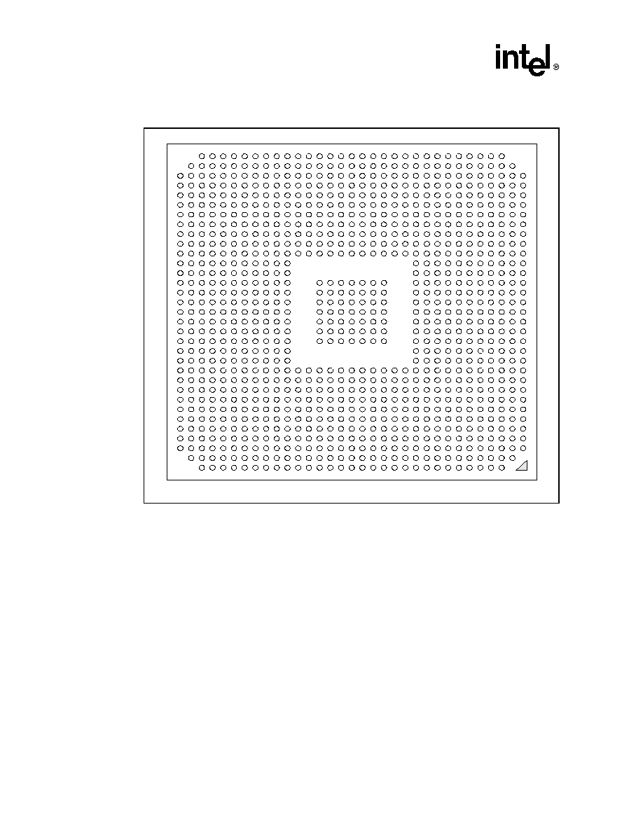
140
Intel
ģ
E7501 Chipset MCH Datasheet
Ballout and Package Specifications
Figure 7-3. MCH Ballout (top view)
AM
AN
AL
AK
AJ
AH
AF
AG
AE
AD
AC
AB
Y
AA
W
V
U
T
P
R
N
M
L
K
H
J
G
F
E
D
C
B
A
AM
AN
AL
AK
AJ
AH
AF
AG
AE
AD
AC
AB
Y
AA
W
V
U
T
P
R
N
M
L
K
H
J
G
F
E
D
C
B
A
33
32
31
30
29
28
27
26
25
24
23
22
21
20
19
18
17
16
15
14
13
12
11
10
9
8
7
6
5
4
3
2
1
33
32
31
30
29
28
27
26
25
24
23
22
21
20
19
18
17
16
15
14
13
12
11
10
9
8
7
6
5
4
3
2
1

Ballout and Package Specifications
Intel
ģ
E7501 Chipset MCH Datasheet
141
Table 7-1. Ballout by
Signal Name
Signal Name
Ball #
ADS#
Y7
AP0#
AJ6
AP1#
AK5
BA_A0
AL31
BA_A1
AH23
BA_B0
K26
BA_B1
H27
BINIT#
AG8
BNR#
V1
BPRI#
U6
BREQ0#
AF9
CAS_A#
AE22
CAS_B#
H28
CB_A0
AE16
CB_A1
AH16
CB_A2
AL16
CB_A3
AK15
CB_A4
AE17
CB_A5
AG17
CB_A6
AM15
CB_A7
AG15
CB_B0
V28
CB_B1
U25
CB_B2
Y31
CB_B3
AA33
CB_B4
U28
CB_B5
U27
CB_B6
AA31
CB_B7
AA32
CKE_A
AE19
CKE_B
M32
CLK66
J16
CMDCLK_A0
AG24
CMDCLK_A0#
AG23
CMDCLK_A1
AJ25
CMDCLK_A1#
AH25
CMDCLK_A2
AG26
CMDCLK_A2#
AF25
CMDCLK_A3
AE25
CMDCLK_A3#
AE24
CMDCLK_B0
J29
CMDCLK_B0#
J28
CMDCLK_B1
L28
CMDCLK_B1#
M28
CMDCLK_B2
J26
CMDCLK_B2#
K25
CMDCLK_B3
K27
CMDCLK_B3#
L27
CPURST#
W9
CS_A0#
AE13
CS_A1#
AK11
CS_A2#
AL10
CS_A3#
AH8
CS_A4#
AN8
CS_A5#
AK7
CS_A6#
AL3
CS_A7#
AL2
CS_B0#
AH29
CS_B1#
AK32
CS_B2#
AF30
CS_B3#
AF27
CS_B4#
AE31
CS_B5#
AE26
CS_B6#
AD28
CS_B7#
Y27
DBI0#
F8
DBI1#
D2
DBI2#
L4
DBI3#
P1
DBSY#
W6
DDRCOMP_A
AH17
DDRCOMP_B
W30
DDRCVO_A
AK17
DDRCVO_B
W32
DDRVREF_A0
AJ7
DDRVREF_A1
AL9
DDRVREF_A2
AM16
DDRVREF_A3
AK21
DDRVREF_B0
AC25
DDRVREF_B1
AG32
DDRVREF_B2
U26
DDRVREF_B3
N33
DEFER#
W8
DP0#
Y4
DP1#
AA2
DP2#
AA5
DP3#
AA4
DQ_A0
AF22
Table 7-1. Ballout by
Signal Name
Signal Name
Ball #
DQ_A1
AN28
DQ_A2
AE21
DQ_A3
AH22
DQ_A4
AN29
DQ_A5
AM28
DQ_A6
AL26
DQ_A7
AL25
DQ_A8
AN25
DQ_A9
AM24
DQ_A10
AG21
DQ_A11
AE20
DQ_A12
AM25
DQ_A13
AK24
DQ_A14
AL22
DQ_A15
AJ22
DQ_A16
AK19
DQ_A17
AL19
DQ_A18
AN17
DQ_A19
AF18
DQ_A20
AN20
DQ_A21
AM19
DQ_A22
AL17
DQ_A23
AJ18
DQ_A24
AF19
DQ_A25
AH19
DQ_A26
AM21
DQ_A27
AL20
DQ_A28
AH20
DQ_A29
AJ21
DQ_A30
AN21
DQ_A31
AJ19
DQ_A32
AL14
DQ_A33
AM13
DQ_A34
AJ15
DQ_A35
AF15
DQ_A36
AK14
DQ_A37
AN13
DQ_A38
AH14
DQ_A39
AG14
DQ_A40
AE14
DQ_A41
AH13
DQ_A42
AN12
DQ_A43
AL11
DQ_A44
AE15
Table 7-1. Ballout by
Signal Name
Signal Name
Ball #

Ballout and Package Specifications
142
Intel
ģ
E7501 Chipset MCH Datasheet
DQ_A45
AF13
DQ_A46
AJ12
DQ_A47
AM10
DQ_A48
AE12
DQ_A49
AH11
DQ_A50
AG11
DQ_A51
AN5
DQ_A52
AG12
DQ_A53
AF12
DQ_A54
AM9
DQ_A55
AM6
DQ_A56
AG10
DQ_A57
AJ9
DQ_A58
AM3
DQ_A59
AM2
DQ_A60
AH10
DQ_A61
AE11
DQ_A62
AL5
DQ_A63
AM4
DQ_B0
F33
DQ_B1
K30
DQ_B2
J32
DQ_B3
N25
DQ_B4
N27
DQ_B5
G32
DQ_B6
M29
DQ_B7
N26
DQ_B8
J33
DQ_B9
K32
DQ_B10
P27
DQ_B11
P25
DQ_B12
J31
DQ_B13
L31
DQ_B14
P26
DQ_B15
P28
DQ_B16
T29
DQ_B17
T30
DQ_B18
U30
DQ_B19
T26
DQ_B20
R32
DQ_B21
T27
DQ_B22
V33
DQ_B23
V31
DQ_B24
P30
Table 7-1. Ballout by
Signal Name
Signal Name
Ball #
DQ_B25
P33
DQ_B26
R26
DQ_B27
T32
DQ_B28
N32
DQ_B29
P31
DQ_B30
R28
DQ_B31
T25
DQ_B32
W27
DQ_B33
AE33
DQ_B34
AF31
DQ_B35
W25
DQ_B36
AA28
DQ_B37
AD32
DQ_B38
AG33
DQ_B39
W26
DQ_B40
AA29
DQ_B41
AB33
DQ_B42
V26
DQ_B43
AD31
DQ_B44
Y28
DQ_B45
AB32
DQ_B46
AB29
DQ_B47
V25
DQ_B48
Y25
DQ_B49
AB27
DQ_B50
AH32
DQ_B51
AH31
DQ_B52
AC28
DQ_B53
AA26
DQ_B54
AG30
DQ_B55
AH33
DQ_B56
AJ30
DQ_B57
AG29
DQ_B58
AB25
DQ_B59
AA25
DQ_B60
AL32
DQ_B61
AJ31
DQ_B62
AC27
DQ_B63
AB26
DQS_A0
AM27
DQS_A1
AL23
DQS_A2
AG18
DQS_A3
AE18
DQS_A4
AL13
Table 7-1. Ballout by
Signal Name
Signal Name
Ball #
DQS_A5
AM12
DQS_A6
AL8
DQS_A7
AL6
DQS_A8
AJ16
DQS_A9
AF21
DQS_A10
AK23
DQS_A11
AK18
DQS_A12
AK20
DQS_A13
AJ13
DQS_A14
AK12
DQS_A15
AM7
DQS_A16
AH9
DQS_A17
AF16
DQS_B0
L30
DQS_B1
M31
DQS_B2
U33
DQS_B3
R29
DQS_B4
AE32
DQS_B5
AC31
DQS_B6
AE28
DQS_B7
AE27
DQS_B8
W29
DQS_B9
H31
DQS_B10
N29
DQS_B11
U31
DQS_B12
R31
DQS_B13
AC30
DQS_B14
AB30
DQS_B15
AD27
DQS_B16
AF28
DQS_B17
Y30
DRDY#
Y3
HA3#
AA8
HA4#
AB1
HA5#
AC3
HA6#
AD2
HA7#
AB6
HA8#
AC4
HA9#
AD4
HA10#
AE5
HA11#
AE2
HA12#
AC6
HA13#
AB9
HA14#
AE6
Table 7-1. Ballout by
Signal Name
Signal Name
Ball #

Ballout and Package Specifications
Intel
ģ
E7501 Chipset MCH Datasheet
143
HA15#
AE3
HA16#
AD5
HA17#
AB8
HA18#
AC7
HA19#
AC9
HA20#
AH2
HA21#
AH3
HA22#
AG2
HA23#
AF6
HA24#
AD8
HA25#
AF1
HA26#
AG4
HA27#
AJ4
HA28#
AE8
HA29#
AF3
HA30#
AF7
HA31#
AH5
HA32#
AG7
HA33#
AH6
HA34#
AJ1
HA35#
AG5
HADSTB0#
AE1
HADSTB1#
AD7
HAVREF0
AF4
HAVREF1
AJ3
HCCVREF
Y6
HCLKINN
U3
HCLKINP
T2
HD0#
B9
HD1#
A9
HD2#
A4
HD3#
B5
HD4#
E8
HD5#
B3
HD6#
A5
HD7#
C8
HD8#
A8
HD9#
C4
HD10#
C7
HD11#
D7
HD12#
H7
HD13#
C2
HD14#
J8
HD15#
J7
Table 7-1. Ballout by
Signal Name
Signal Name
Ball #
HD16#
F7
HD17#
L7
HD18#
L6
HD19#
E6
HD20#
G6
HD21#
D6
HD22#
F5
HD23#
E4
HD24#
M8
HD25#
E1
HD26#
F4
HD27#
D3
HD28#
F2
HD29#
E3
HD30#
F1
HD31#
M7
HD32#
H4
HD33#
H3
HD34#
G2
HD35#
K3
HD36#
G3
HD37#
J1
HD38#
K2
HD39#
K1
HD40#
N6
HD41#
J5
HD42#
P9
HD43#
M4
HD44#
P7
HD45#
N7
HD46#
R7
HD47#
R8
HD48#
L3
HD49#
N4
HD50#
P4
HD51#
M2
HD52#
L2
HD53#
N2
HD54#
N3
HD55#
N1
HD56#
R2
HD57#
T6
HD58#
T3
HD59#
U7
Table 7-1. Ballout by
Signal Name
Signal Name
Ball #
HD60#
T9
HD61#
T5
HD62#
R5
HD63#
T8
HDSTBN0#
B6
HDSTBN1#
K6
HDSTBN2#
J2
HDSTBN3#
R4
HDSTBP0#
B8
HDSTBP1#
H6
HDSTBP2#
J4
HDSTBP3#
P3
HDVREF0
C5
HDVREF1
N8
HDVREF2
P6
HDVREF3
T7
HI_A0
E11
HI_A1
B11
HI_A2
G10
HI_A3
F10
HI_A4
D9
HI_A5
E9
HI_A6
J11
HI_A7
H9
HI_A8
J13
HI_A9
J10
HI_A10
F11
HI_A11
G12
HI_B0
D16
HI_B1
G16
HI_B2
C17
HI_B3
C16
HI_B4
A17
HI_B5
A16
HI_B6
B14
HI_B7
D15
HI_B8
C14
HI_B9
F13
HI_B10
A13
HI_B11
C13
HI_B12
D12
HI_B13
E12
HI_B14
C11
HI_B15
J14
Table 7-1. Ballout by
Signal Name
Signal Name
Ball #

Ballout and Package Specifications
144
Intel
ģ
E7501 Chipset MCH Datasheet
HI_B16
H14
HI_B17
B17
HI_B18
E14
HI_B20
F14
HI_B21
G13
HI_C0
D22
HI_C1
B24
HI_C2
G18
HI_C3
C22
HI_C4
E20
HI_C5
F19
HI_C6
D21
HI_C7
E21
HI_C8
D19
HI_C9
A20
HI_C10
B20
HI_C11
C19
HI_C12
B18
HI_C13
C18
HI_C14
E18
HI_C15
F17
HI_C16
B21
HI_C17
C24
HI_C18
F20
HI_C20
H18
HI_C21
F16
HI_D0
D28
HI_D1
G25
HI_D2
G26
HI_D3
F26
HI_D4
G24
HI_D5
A27
HI_D6
H24
HI_D7
C26
HI_D8
G22
HI_D9
E24
HI_D10
A25
HI_D11
D24
HI_D12
A24
HI_D13
E23
HI_D14
F23
HI_D15
F22
HI_D16
H23
HI_D17
H25
Table 7-1. Ballout by
Signal Name
Signal Name
Ball #
HI_D18
F25
HI_D20
E27
HI_D21
H21
HIRCOMP_A
H11
HIRCOMP_B
E15
HIRCOMP_C
C20
HIRCOMP_D
G21
HISWNG_A
H12
HISWNG_B
B15
HISWNG_C
H17
HISWNG_D
F24
HIT#
U1
HITM#
W5
HIVREF_A
G9
HIVREF_B
D13
HIVREF_C
A21
HIVREF_D
J22
HLOCK#
V7
HREQ0#
AB2
HREQ1#
AA1
HREQ2#
AA7
HREQ3#
AB3
HREQ4#
Y9
HTRDY#
W3
HXRCOMP
V4
HXSWNG
V8
HYRCOMP
G5
HYSWNG
K5
MA_A0
AF24
MA_A1
AK26
MA_A2
AH26
MA_A3
AJ27
MA_A4
AG27
MA_A5
AH28
MA_A6
AL28
MA_A7
AL29
MA_A8
AK29
MA_A9
AM30
MA_A10
AJ24
MA_A11
AK30
MA_A12
AM31
MA_B0
M26
MA_B1
K29
MA_B2
H30
Table 7-1. Ballout by
Signal Name
Signal Name
Ball #
MA_B3
G30
MA_B4
F32
MA_B5
G29
MA_B6
F31
MA_B7
E33
MA_B8
E31
MA_B9
F29
MA_B10
L25
MA_B11
C31
MA_B12
C32
NC
AN16
NC
V29
NC
AM22
NC
N30
ODTCOMP
AJ28
PSTRBF_A
C10
PSTRBS_A
D10
PSTRBF_B
G15
PSTRBS_B
H15
PSTRBF_C
C23
PSTRBS_C
B23
PSTRBF_D
D27
PSTRBS_D
D26
PUSTRBF_B
A12
PUSTRBS_B
B12
PUSTRBF_C
D18
PUSTRBS_C
E17
PUSTRBF_D
B25
PUSTRBS_D
C25
PWRGOOD
A28
RAS_A#
AN24
RAS_B#
V32
RCVEN_A
AG20
RCVEN_B
R25
Reserved
AK27
Reserved
M25
Reserved
E30
Reserved
B30
Reserved
AM18
Reserved
K33
Reserved
D29
RS0#
V2
RS1#
V5
RS2#
U4
Table 7-1. Ballout by
Signal Name
Signal Name
Ball #

Ballout and Package Specifications
Intel
ģ
E7501 Chipset MCH Datasheet
145
RSP#
AK4
RSTIN#
E28
SMB_CLK
J25
SMB_DATA
B31
VCC_CPU
AC5
VCC_CPU
AG3
VCC_CPU
AJ5
VCC_CPU
AF5
VCC_CPU
AH1
VCC_CPU
K7
VCC_CPU
F3
VCC_CPU
P5
VCC_CPU
R3
VCC_CPU
W7
VCC_CPU
H5
VCC_CPU
L5
VCC_CPU
U5
VCC_CPU
Y5
VCC_CPU
AE7
VCC_CPU
K9
VCC_CPU
AD1
VCC_CPU
D1
VCC_CPU
H1
VCC_CPU
M1
VCC_CPU
T1
VCC_CPU
Y1
VCC_CPU
A6
VCC_CPU
E7
VCC_CPU
AA10
VCC_CPU
AB11
VCC_CPU
AC10
VCC_CPU
C3
VCC_CPU
D5
VCC_CPU
L10
VCC_CPU
M11
VCC_CPU
N10
VCC_CPU
P11
VCC_CPU
R10
VCC_CPU
T11
VCC_CPU
U10
VCC_CPU
V11
VCC_CPU
W10
VCC_CPU
Y11
VCC1_2
L18
Table 7-1. Ballout by
Signal Name
Signal Name
Ball #
VCC1_2
L20
VCC1_2
L22
VCC1_2
B28
VCC1_2
H20
VCC1_2
A10
VCC1_2
A14
VCC1_2
A18
VCC1_2
A22
VCC1_2
E10
VCC1_2
E13
VCC1_2
E16
VCC1_2
E19
VCC1_2
E22
VCC1_2
K13
VCC1_2
K15
VCC1_2
K17
VCC1_2
K19
VCC1_2
K21
VCC1_2
K23
VCC1_2
P14
VCC1_2
P18
VCC1_2
R17
VCC1_2
R19
VCC1_2
T14
VCC1_2
T16
VCC1_2
T18
VCC1_2
U17
VCC1_2
U19
VCC1_2
V16
VCC1_2
V18
VCC1_2
W15
VCC1_2
W17
VCC1_2
W19
VCC1_2
A26
VCC1_2
A30
VCC1_2
R15
VCC1_2
V14
VCC1_2
E26
VCC1_2
H19
VCC1_2
K11
VCC1_2
L12
VCC1_2
L14
VCC1_2
L16
VCC2_5
R23
Table 7-1. Ballout by
Signal Name
Signal Name
Ball #
VCC2_5
AN4
VCC2_5
AN7
VCC2_5
AA23
VCC2_5
AC13
VCC2_5
AC15
VCC2_5
AC17
VCC2_5
AC19
VCC2_5
U23
VCC2_5
W23
VCC2_5
AB24
VCC2_5
AD12
VCC2_5
AD14
VCC2_5
AD16
VCC2_5
AD18
VCC2_5
AD20
VCC2_5
AD25
VCC2_5
AD29
VCC2_5
AD33
VCC2_5
AE10
VCC2_5
AE30
VCC2_5
AF33
VCC2_5
AJ11
VCC2_5
AJ14
VCC2_5
AJ17
VCC2_5
AJ20
VCC2_5
AJ23
VCC2_5
AK33
VCC2_5
AN10
VCC2_5
AN14
VCC2_5
AN18
VCC2_5
AN22
VCC2_5
AN26
VCC2_5
H33
VCC2_5
L29
VCC2_5
M33
VCC2_5
P24
VCC2_5
P29
VCC2_5
T24
VCC2_5
T33
VCC2_5
U29
VCC2_5
V24
VCC2_5
Y24
VCC2_5
Y29
VCC2_5
Y33
Table 7-1. Ballout by
Signal Name
Signal Name
Ball #

Ballout and Package Specifications
146
Intel
ģ
E7501 Chipset MCH Datasheet
VCC2_5
AA27
VCC2_5
AG13
VCC2_5
AG19
VCC2_5
AG22
VCC2_5
AK10
VCC2_5
AK8
VCC2_5
AL1
VCC2_5
AL15
VCC2_5
AL24
VCC2_5
G27
VCC2_5
AC21
VCC2_5
AC23
VCC2_5
L23
VCC2_5
N23
VCC2_5
AD22
VCC2_5
AD24
VCC2_5
AJ26
VCC2_5
AJ29
VCC2_5
AN30
VCC2_5
D33
VCC2_5
E29
VCC2_5
H29
VCC2_5
K24
VCC2_5
M24
VCC2_5
AF23
VCC2_5
AG28
VCC2_5
AM32
VCC2_5
B32
VCC2_5
L26
VCC2_5
AB31
VCC2_5
K31
VCC2_5
T31
VCCA1_2
P20
VCCA1_2
T20
VCCA1_2
V20
VCCA1_2
Y14
VCCA1_2
Y16
VCCA1_2
Y18
VCCA1_2
Y20
VCCACPU1_2
U15
VCCAHI1_2
P16
VSS
AD11
VSS
AD13
VSS
AD15
Table 7-1. Ballout by
Signal Name
Signal Name
Ball #
VSS
AD17
VSS
AD19
VSS
AD21
VSS
AD23
VSS
AD26
VSS
AD30
VSS
AE29
VSS
AE9
VSS
AF10
VSS
AF11
VSS
AF14
VSS
AF17
VSS
AF20
VSS
AF26
VSS
AF29
VSS
AF32
VSS
AG16
VSS
AG25
VSS
AG31
VSS
AH12
VSS
AH15
VSS
AH18
VSS
AH21
VSS
AH24
VSS
AH27
VSS
AH30
VSS
AJ32
VSS
AJ33
VSS
AK13
VSS
AK16
VSS
AK22
VSS
AK25
VSS
AK28
VSS
AK31
VSS
AL12
VSS
AL18
VSS
AL21
VSS
AL27
VSS
AL30
VSS
AL33
VSS
AM11
VSS
AM14
VSS
AM17
VSS
AM20
Table 7-1. Ballout by
Signal Name
Signal Name
Ball #
VSS
AM23
VSS
AM26
VSS
AM29
VSS
AN11
VSS
AK9
VSS
AM8
VSS
AC8
VSS
G7
VSS
D30
VSS
AF8
VSS
AA9
VSS
J6
VSS
V3
VSS
F28
VSS
AG6
VSS
AH7
VSS
AH4
VSS
AN15
VSS
AN19
VSS
AN23
VSS
AN27
VSS
AN3
VSS
AN31
VSS
AN6
VSS
B10
VSS
B13
VSS
B16
VSS
B19
VSS
B22
VSS
B26
VSS
B29
VSS
B4
VSS
B7
VSS
C1
VSS
C12
VSS
C15
VSS
C21
VSS
C27
VSS
C30
VSS
C33
VSS
C6
VSS
C9
VSS
D11
VSS
D14
Table 7-1. Ballout by
Signal Name
Signal Name
Ball #

Ballout and Package Specifications
Intel
ģ
E7501 Chipset MCH Datasheet
147
VSS
D17
VSS
D20
VSS
D23
VSS
D31
VSS
D8
VSS
E25
VSS
E32
VSS
F12
VSS
F15
VSS
F18
VSS
F21
VSS
F27
VSS
F30
VSS
F6
VSS
F9
VSS
G1
VSS
G11
VSS
G14
VSS
G17
VSS
G20
VSS
G23
VSS
G28
VSS
G31
VSS
G33
VSS
AL4
VSS
AJ2
VSS
AK3
VSS
AD6
VSS
AK6
VSS
AL7
VSS
AM5
VSS
AF2
VSS
AD3
VSS
AG1
VSS
AK1
VSS
U9
VSS
E2
VSS
H2
VSS
K4
VSS
J3
VSS
K8
VSS
L8
VSS
G4
VSS
M6
Table 7-1. Ballout by
Signal Name
Signal Name
Ball #
VSS
P2
VSS
M3
VSS
M9
VSS
P8
VSS
N9
VSS
U2
VSS
R6
VSS
T4
VSS
V6
VSS
W4
VSS
W2
VSS
Y2
VSS
AA3
VSS
AA6
VSS
Y8
VSS
J19
VSS
J20
VSS
G19
VSS
E5
VSS
J23
VSS
AB5
VSS
D4
VSS
AE4
VSS
AC2
VSS
AG9
VSS
L9
VSS
C28
VSS
B27
VSS
AB4
VSS
AB7
VSS
AD9
VSS
G8
VSS
H10
VSS
H13
VSS
H16
VSS
H22
VSS
H26
VSS
H32
VSS
H8
VSS
J12
VSS
J15
VSS
J18
VSS
J21
VSS
J24
Table 7-1. Ballout by
Signal Name
Signal Name
Ball #
VSS
J27
VSS
J30
VSS
J9
VSS
K12
VSS
K14
VSS
K16
VSS
K18
VSS
K20
VSS
K22
VSS
K28
VSS
L1
VSS
L24
VSS
L32
VSS
L33
VSS
M23
VSS
M27
VSS
M30
VSS
N5
VSS
N24
VSS
N28
VSS
N31
VSS
P15
VSS
P17
VSS
P19
VSS
P23
VSS
P32
VSS
R1
VSS
R14
VSS
R18
VSS
R20
VSS
R24
VSS
R27
VSS
R30
VSS
R33
VSS
R9
VSS
T15
VSS
T17
VSS
T19
VSS
AA11
VSS
AB10
VSS
AC11
VSS
AD10
VSS
AN9
VSS
M10
Table 7-1. Ballout by
Signal Name
Signal Name
Ball #

Ballout and Package Specifications
148
Intel
ģ
E7501 Chipset MCH Datasheet
VSS
M5
VSS
N11
VSS
P10
VSS
R11
VSS
T10
VSS
U11
VSS
V10
VSS
W11
VSS
Y10
VSS
B2
VSS
J17
VSS
K10
VSS
L11
VSS
L13
VSS
L15
VSS
L17
VSS
L19
VSS
L21
VSS
R16
VSS
AC29
VSS
AJ10
VSS
D25
VSS
A11
VSS
A15
VSS
A19
VSS
A23
VSS
A29
Table 7-1. Ballout by
Signal Name
Signal Name
Ball #
VSS
A3
VSS
A31
VSS
A7
VSS
AA24
VSS
AA30
VSS
AB23
VSS
AB28
VSS
AC1
VSS
AC12
VSS
AC14
VSS
AC16
VSS
AC18
VSS
AC20
VSS
AC22
VSS
AC24
VSS
AC26
VSS
AC32
VSS
AC33
VSS
T23
VSS
T28
VSS
U14
VSS
U16
VSS
U18
VSS
U20
VSS
U24
VSS
U32
VSS
U8
Table 7-1. Ballout by
Signal Name
Signal Name
Ball #
VSS
V15
VSS
V17
VSS
V19
VSS
V23
VSS
V27
VSS
V30
VSS
V9
VSS
W1
VSS
W14
VSS
W16
VSS
W18
VSS
W20
VSS
W24
VSS
W28
VSS
W31
VSS
W33
VSS
Y15
VSS
Y17
VSS
Y19
VSS
Y23
VSS
Y26
VSS
Y32
VSS
AJ8
WE_A#
AE23
WE_B#
D32
XERR#
AK2
XORMODE#
C29
Table 7-1. Ballout by
Signal Name
Signal Name
Ball #

Intel
ģ
E7501 Chipset MCH Datasheet
149
Ballout and Package Specifications
7.2
Package Specifications
Figure 7-4
and
Figure 7-5
provide the package specifications for the MCH.
NOTE:
1. All dimensions are in millimeters.
2. All dimensions and tolerances conform to ANSI Y14.5M-1982.
Figure 7-4. MCH Package Dimensions (Top View)
AN
AM
AL
AK
AJ
AH
AG
AF
AE
AD
AC
AB
AA
Y
W
V
U
T
R
P
N
M
L
K
J
H
G
F
E
D
C
B
A
10
16
20
3
5
7
9
11
13
15
19
4
6
18
8
12
14
22
21
24 23
26
25
28
27
30 29
31
32
(n)x 0.025 Min
Metal Edge
(n)x
0.790 Ī 0.025
Solder Resist Opening
(n)x 0.650 Ī 0.040
Detail A
00.071 L C
00.200 L C A S B
33
1
2
1.270
20.320
40.640
2x 42.500 Ī0.100
0.200 A B
1.270
21.250
Detail A
Pk
T
Vi
17

150
Intel
ģ
E7501 Chipset MCH Datasheet
Ballout and Package Specifications
NOTES:
1. All dimensions are in millimeters.
2. Substrate thickness and package overall height are thicker than standard 492-L-PBGA
3. Primary datum --C-- and seating plane are defined by the spherical crowns of the solder balls.
4. All dimensions and tolerances conform to ANSI Y14.5M-1982.
Figure 7-5. MCH Package Dimensions (Side View)
1.10 Ī 0.10 mm
Die
Substrate
0.60 Ī 0.10 mm
Seating Plane
1.940 Ī 0.150 mm
0.20
≠C≠
See note 3.

Intel
ģ
E7501 Chipset MCH Datasheet
151
Ballout and Package Specifications
7.3
Chipset Interface Trace Length Compensation
In this section, detailed information is given about the internal component package trace lengths to
enable trace length compensation. Trace length compensation is required for platform design.
These lengths must be considered when matching trace lengths as described in the Intel
ģ
XeonTM
Processor and Intel
ģ
E7500 / E7501 Chipset Compatible Platform Design Guide. Note that these
lengths represent the actual lengths from pad to ball.
Note: Different length matching requirements must be followed for each platform interface. These
guidelines are specified in the corresponding sections of the platform design guide. Use of the
Length Matching Spreadsheet is recommended to provide lengths for major interfaces. Contact
your Intel representative for information about the Length Matching Spreadsheet tool.
The data given can be normalized from a particular reference ball to simplify routing. If the longest
trace is used as the reference for normalization, use the following equation:
Equation 7-1.
∑
L
REF
is the nominal package length of the reference signal used for normalization.
∑
ńL
PKG
is the nominal ń package trace length of the MCH from the reference trace.
To calculate the ńL
PCB
for signals from the MCH to the device, use the following formula.
Equation 7-2.
∑
ńL
PCB
is the nominal ń PCB trace length to be added on the PCB.
∑
ńL
PKG
is the nominal ń package trace length of the MCH (refer to Equation 1).
∑
V
PKG
is the MCH package trace delay due to signal velocity. The nominal value is 150 ps/in.
∑
V
PCB
is the PCB trace delay due to signal velocity. The nominal value is 175 ps/in on the
recommended stackup.
Note: Use care when converting delays and velocities (x ps/in is a delay, y in/ps is a velocity).
Table 7-2
shows example values when signal MEMORY1 trace length is used for normalization.
PKG
REF
PKG
L
L
L
-
=
PCB
PKG
PKG
PCB
V
V
L
L
◊
=
Table 7-2. Example Normalization Table
L
PKG
(mils)
L
PKG
(mils)
L
PCB
(mils)
Target L
PCB
(mils)
MEMORY1
175.984
0.000
0.000
3500.000
MEMORY2
152.364
23.620
20.246
3520.246
MEMORY3
130.315
45.669
39.145
3539.145
MEMORY4
118.897
57.087
48.932
3548.932
MEMORYN
102.756
73.228
62.767
3562.767

152
Intel
ģ
E7501 Chipset MCH Datasheet
Ballout and Package Specifications
7.3.1
System Bus Signal Package Trace Length Data
Table 7-3
provides the MCH package trace length information for the system bus.
Table 7-3. MCH L
PKG
Data for the System Bus (Sheet 1 of 2)
Signal
Ball No.
L
PKG
(mils)
Signal
Ball No.
L
PKG
(mils)
HADSTB0#
AE1
796.57
HDSTBN0#
B6
841.53
HA3#
AA8
292.76
HDSTBP0#
B8
738.27
HA4#
AB1
690.67
HD0#
B9
680.98
HA5#
AC3
600.79
HD1#
A9
774.60
HA6#
AD2
760.04
HD2#
A4
953.78
HA7#
AB6
470.04
HD3#
B5
931.65
HA8#
AC4
567.56
HD4#
E8
645.47
HA9#
AD4
630.00
HD5#
B3
1042.71
HA10#
AE5
610.71
HD6#
A5
929.45
HA11#
AE2
780.51
HD7#
C8
732.32
HA12#
AC6
472.52
HD8#
A8
762.12
HA13#
AB9
574.64
HD9#
C4
907.68
HA14#
AE6
575.24
HD10#
C7
777.68
HA15#
AE3
701.14
HD11#
D7
763.38
HA16#
AD5
511.42
HD12#
H7
534.25
HREQ0#
AB2
662.09
HD13#
C2
1058.50
HREQ1#
AA1
683.38
HD14#
J8
398.54
HREQ2#
AA7
394.37
HD15#
J7
456.26
HREQ3#
AB3
588.07
DBI0#
F8
592.64
HREQ4#
Y9
304.88
HDSTBN1#
K6
478.90
HADSTB1#
AD7
431.81
HDSTBP1#
H6
560.94
HA17#
AB8
331.34
HD16#
F7
616.26
HA18#
AC7
389.09
HD17#
L7
377.52
HA19#
AC9
376.22
HD18#
L6
448.58
HA20#
AH2
859.09
HD19#
E6
761.18
HA21#
AH3
730.63
HD20#
G6
678.78
HA22#
AG2
770.71
HD21#
D6
770.27
HA23#
AF6
566.30
HD22#
F5
808.23
HA24#
AD8
400.12
HD23#
E4
858.23
HA25#
AF1
797.05
HD24#
M8
331.30
HA26#
AG4
689.29
HD25#
E1
1028.78
HA27#
AJ4
693.94
HD26#
F4
850.08
HA28#
AE8
411.61
HD27#
D3
891.18

Intel
ģ
E7501 Chipset MCH Datasheet
153
Ballout and Package Specifications
HA29#
AF3
734.64
HD28#
F2
943.62
HA30#
AF7
519.96
HD29#
E3
903.70
HA31#
AH5
618.27
HD30#
F1
1029.53
HA32#
AG7
495.90
HD31#
M7
397.13
HA33#
AH6
600.27
DBI1#
D2
980.27
HA34#
AJ1
876.45
HA35#
AG5
610.31
HCLKINN
U3
630.08
HCLKINP
T2
630.04
HDSTBN2#
J2
781.73
HDSTBN3#
R4
526.02
HDSTBP2#
J4
717.52
HDSTBP3#
P3
602.32
HD32#
H4
714.01
HD48#
L3
667.95
HD33#
H3
801.57
HD49#
N4
596.10
HD34#
G2
863.82
HD50#
P4
581.42
HD35#
K3
722.32
HD51#
M2
719.53
HD36#
G3
816.85
HD52#
L2
727.72
HD37#
J1
802.09
HD53#
N2
704.09
HD38#
K2
738.82
HD54#
N3
602.52
HD39#
K1
820.08
HD55#
N1
758.58
HD40#
N6
415.98
HD56#
R2
610.04
HD41#
J5
723.82
HD57#
T6
530.87
HD42#
P9
306.10
HD58#
T3
576.81
HD43#
M4
619.25
HD59#
U7
364.17
HD44#
P7
369.96
HD60#
T9
268.07
HD45#
N7
347.91
HD61#
T5
475.79
HD46#
R7
332.16
HD62#
R5
448.07
HD47#
R8
308.74
HD63#
T8
309.49
DBI2#
L4
648.23
DBI3#
P1
685.35
Table 7-3. MCH L
PKG
Data for the System Bus (Sheet 2 of 2)
Signal
Ball No.
L
PKG
(mils)
Signal
Ball No.
L
PKG
(mils)

154
Intel
ģ
E7501 Chipset MCH Datasheet
Ballout and Package Specifications
7.3.2
MCH DDR Channel A Signal Package Trace Length Data
Table 7-4
provides the MCH package trace length information for channel A of the DDR memory
interface.
Table 7-4. MCH L
PKG
Data for DDR Channel A (Sheet 1 of 2)
Signal
Ball No.
L
PKG
(mils)
Signal
Ball No.
L
PKG
(mils)
DQS_A0
AM27
816.53
DQS_A2
AG18
356.06
DQS_A9
AF21
417.05
DQS_A11
AK18
567.48
DQ_A0
AF22
388.74
DQ_A16
AK19
534.01
DQ_A1
AN28
900.90
DQ_A17
AL19
607.28
DQ_A2
AE21
391.50
DQ_A18
AN17
697.83
DQ_A3
AH22
599.96
DQ_A19
AF18
332.32
DQ_A4
AN29
907.40
DQ_A20
AN20
690.51
DQ_A5
AM28
862.71
DQ_A21
AM19
624.96
DQ_A6
AL26
747.52
DQ_A22
AL17
617.05
DQ_A7
AL25
682.99
DQ_A23
AJ18
450.63
DQS_A1
AL23
634.49
DQS_A3
AE18
375.51
DQS_A10
AK23
579.13
DQS_A12
AK20
591.14
DQ_A8
AN25
813.07
DQ_A24
AF19
395.00
DQ_A9
AM24
730.86
DQ_A25
AH19
516.81
DQ_A10
AG21
413.15
DQ_A26
AM21
747.52
DQ_A11
AE20
345.79
DQ_A27
AL20
666.30
DQ_A12
AM25
752.40
DQ_A28
AH20
535.43
DQ_A13
AK24
616.53
DQ_A29
AJ21
630.27
DQ_A14
AL22
599.92
DQ_A30
AN21
813.58
DQ_A15
AJ22
485.83
DQ_A31
AJ19
529.21
DQS_A4
AL13
617.09
DQS_A7
AL6
757.56
DQS_A13
AJ13
544.53
DQS_A16
AH9
572.24
DQ_A32
AL14
627.09
DQ_A56
AG10
486.38
DQ_A33
AM13
687.40
DQ_A57
AJ9
594.72
DQ_A34
AJ15
559.80
DQ_A58
AM3
962.48
DQ_A35
AF15
405.67
DQ_A59
AM2
985.43
DQ_A36
AK14
604.64
DQ_A60
AH10
527.32
DQ_A37
AN13
729.25
DQ_A61
AE11
389.01
DQ_A38
AH14
489.88
DQ_A62
AL5
795.23
DQ_A39
AG14
412.52
DQ_A63
AM4
884.88
Intel
ģ
E7501 Chipset MCH Datasheet
155
Ballout and Package Specifications
DQS_A5
AM12
778.27
DQS_A8
AJ16
544.33
DQS_A14
AK12
610.59
DQS_A17
AF16
347.28
DQ_A40
AE14
479.84
CB_A0
AE16
345.55
DQ_A41
AH13
531.53
CB_A1
AH16
520.35
DQ_A42
AN12
782.52
CB_A2
AL16
684.01
DQ_A43
AL11
752.83
CB_A3
AK15
647.24
DQ_A44
AE15
402.91
CB_A4
AE17
422.52
DQ_A45
AF13
478.90
CB_A5
AG17
392.44
DQ_A46
AJ12
582.64
CB_A6
AM15
717.48
DQ_A47
AM10
801.42
CB_A7
AG15
457.24
DQS_A6
AL8
717.01
CMDCLK_A0
AG24
568.46
DQS_A15
AM7
800.86
CMDCLK_A0#
AG23
518.54
DQ_A48
AE12
372.09
CMDCLK_A1
AJ25
621.81
DQ_A49
AH11
523.86
CMDCLK_A1#
AH25
559.13
DQ_A50
AG11
529.57
CMDCLK_A2
AG26
559.53
DQ_A51
AN5
937.56
CMDCLK_A2#
AF25
467.44
DQ_A52
AG12
455.98
CMDCLK_A3
AE25
374.80
DQ_A53
AF12
416.30
CMDCLK_A3#
AE24
338.03
DQ_A54
AM9
786.42
DQ_A55
AM6
895.98
Table 7-4. MCH L
PKG
Data for DDR Channel A (Sheet 2 of 2)
Signal
Ball No.
L
PKG
(mils)
Signal
Ball No.
L
PKG
(mils)

156
Intel
ģ
E7501 Chipset MCH Datasheet
Ballout and Package Specifications
7.3.3
MCH DDR Channel B Signal Package Trace Length Data
Table 7-5
provides the MCH package trace length information for channel B of the DDR memory
interface.
Table 7-5. MCH L
PKG
Data for DDR Channel B (Sheet 1 of 2)
Signal
Ball No.
L
PKG
(mils)
Signal
Ball No.
L
PKG
(mils)
DQS_B0
L30
658.35
DQS_B3
R29
505.35
DQS_B9
H31
785.27
DQS_B12
R31
666.97
DQ_B0
F33
950.79
DQ_B24
P30
567.56
DQ_B1
K30
747.99
DQ_B25
P33
765.16
DQ_B2
J32
780.83
DQ_B26
R26
380.90
DQ_B3
N25
415.39
DQ_B27
T32
707.28
DQ_B4
N27
453.90
DQ_B28
N32
702.75
DQ_B5
G32
885.31
DQ_B29
P31
634.96
DQ_B6
M29
583.27
DQ_B30
R28
485.24
DQ_B7
N26
440.24
DQ_B31
T25
343.42
DQS_B1
M31
687.95
DQS_B4
AE32
805.23
DQS_B10
N29
534.96
DQS_B13
AC30
669.21
DQ_B8
J33
833.11
DQ_B32
W27
407.40
DQ_B9
K32
791.81
DQ_B33
AE33
853.70
DQ_B10
P27
440.12
DQ_B34
AF31
824.01
DQ_B11
P25
375.55
DQ_B35
W25
625.51
DQ_B12
J31
776.77
DQ_B36
AA28
516.10
DQ_B13
L31
739.37
DQ_B37
AD32
749.21
DQ_B14
P26
424.17
DQ_B38
AG33
842.95
DQ_B15
P28
499.29
DQ_B39
W26
341.73
DQS_B2
U33
696.85
DQS_B5
AC31
791.22
DQS_B11
U31
606.69
DQS_B14
AB30
751.49
DQ_B16
T29
504.05
DQ_B40
AA29
684.05
DQ_B17
T30
556.06
DQ_B41
AB33
832.40
DQ_B18
U30
554.92
DQ_B42
V26
408.03
DQ_B19
T26
349.41
DQ_B43
AD31
819.76
DQ_B20
R32
678.27
DQ_B44
Y28
562.60
DQ_B21
T27
391.30
DQ_B45
AB32
810.43
DQ_B22
V33
691.34
DQ_B46
AB29
655.79
DQ_B23
V31
571.34
DQ_B47
V25
700.39

Intel
ģ
E7501 Chipset MCH Datasheet
157
Ballout and Package Specifications
DQS_B6
AE28
628.50
DQS_B8
W29
593.94
DQS_B15
AD27
575.04
DQS_B17
Y30
674.13
DQ_B48
Y25
288.31
CB_B0
V28
517.52
DQ_B49
AB27
450.75
CB_B1
U25
365.90
DQ_B50
AH32
881.06
CB_B2
Y31
723.03
DQ_B51
AH31
863.46
CB_B3
AA33
796.89
DQ_B52
AC28
532.28
CB_B4
U28
469.61
DQ_B53
AA26
345.24
CB_B5
U27
443.46
DQ_B54
AG30
788.23
CB_B6
AA31
652.24
DQ_B55
AH33
938.07
CB_B7
AA32
753.11
DQS_B7
AE27
531.97
CMDCLK_B0
J29
541.26
DQS_B16
AF28
626.65
CMDCLK_B0#
J28
485.00
DQ_B56
AJ30
807.44
CMDCLK_B1
L28
518.31
DQ_B57
AG29
688.07
CMDCLK_B1#
M28
506.53
DQ_B58
AB25
463.23
CMDCLK_B2
J26
466.10
DQ_B59
AA25
301.73
CMDCLK_B2#
K25
381.61
DQ_B60
AL32
908.78
CMDCLK_B3
K27
580.63
DQ_B61
AJ31
804.49
CMDCLK_B3#
L27
557.72
DQ_B62
AC27
478.94
DQ_B63
AB26
356.85
Table 7-5. MCH L
PKG
Data for DDR Channel B (Sheet 2 of 2)
Signal
Ball No.
L
PKG
(mils)
Signal
Ball No.
L
PKG
(mils)

158
Intel
ģ
E7501 Chipset MCH Datasheet
Ballout and Package Specifications
7.3.4
MCH Hub Interface_B Signal Package Trace Length Data
Table 7-6
provides the MCH package trace length information for Hub Interface_B.
7.3.5
MCH Hub Interface_C Signal Package Trace Length Data
Table 7-7
provides the MCH package trace length information for Hub Interface_C.
Table 7-6. MCH L
PKG
Data for Hub Interface_B
Signal
Ball No.
L
PKG
(mils)
Signal
Ball No.
L
PKG
(mils)
PSTRBF_B
G15
332.36
PUSTRBF_B
A12
665.47
PSTRBS_B
H15
298.90
PUSTRBS_B
B12
644.33
HI_B0
D16
481.42
HI_B8
C14
590.12
HI_B1
G16
474.88
HI_B9
F13
431.77
HI_B2
C17
543.11
HI_B10
A13
692.75
HI_B3
C16
570.12
HI_B11
C13
565.39
HI_B4
A17
674.05
HI_B12
D12
517.09
HI_B5
A16
670.86
HI_B13
E12
503.11
HI_B6
B14
595.98
HI_B14
C11
610.31
HI_B7
D15
529.61
HI_B15
J14
268.74
HI_B20
F14
413.11
HI_B21
G13
384.96
Table 7-7. MCH L
PKG
Data for Hub Interface_C
Signal
Ball No.
L
PKG
(mils)
Signal
Ball No.
L
PKG
(mils)
PSTRBF_C
C23
679.64
PUSTRBF_C
D18
513.38
PSTRBS_C
B23
731.06
PUSTRBS_C
E17
463.42
HI_C0
D22
633.74
HI_C8
D19
555.79
HI_C1
B24
756.49
HI_C9
A20
717.12
HI_C2
G18
359.53
HI_C10
B20
664.29
HI_C3
C22
694.84
HI_C11
C19
615.08
HI_C4
E20
494.01
HI_C12
B18
649.05
HI_C5
F19
393.42
HI_C13
C18
560.35
HI_C6
D21
608.15
HI_C14
E18
452.52
HI_C7
E21
515.27
HI_C15
F17
378.19
HI_C20
H18
293.19
HI_C21
F16
415.04

Intel
ģ
E7501 Chipset MCH Datasheet
159
Ballout and Package Specifications
7.3.6
MCH Hub Interface_D Signal Package Trace Length Data
Table 7-8
provides the MCH package trace length information for Hub Interface_D.
Table 7-8. MCH L
PKG
Data for Hub Interface_D
Signal
Ball No.
L
PKG
(mils)
Signal
Ball No.
L
PKG
(mils)
PSTRBF_D
D27
717.68
PUSTRBF_D
B25
758.58
PSTRBS_D
D26
730.08
PUSTRBS_D
C25
714.68
HI_D0
D28
772.60
HI_D8
G22
492.64
HI_D1
G25
562.64
HI_D9
E24
587.16
HI_D2
G26
536.77
HI_D10
A25
814.64
HI_D3
F26
592.64
HI_D11
D24
617.44
HI_D4
G24
513.82
HI_D12
A24
807.24
HI_D5
A27
901.06
HI_D13
E23
525.12
HI_D6
H24
415.12
HI_D14
F23
492.87
HI_D7
C26
741.30
HI_D15
F22
495.63
HI_D20
E27
698.38
HI_D21
H21
499.01

160
Intel
ģ
E7501 Chipset MCH Datasheet
Ballout and Package Specifications
This page is intentionally left blank.

Intel
ģ
E7501 Chipset MCH Datasheet
161
Testability
Testability
8
For Automated Test Equipment (ATE) the MCH supports XOR-tree testing. XOR-tree testing
allows board-level interconnections to be tested. An XOR-Tree is a chain of XOR gates, with each
having one input pin or one bi-directional pin (used as an input pin only) connected to it.
8.1
XORMODE# Usage
The XORMODE# is a test input. The MCH enters XORMODE# for board level testing. When the
following conditions are met, the MCH will be in XOR-test. If any of the following are not met,
then XOR-test will not be enabled.
1. Assert PWRGD.
2. Assert RSTIN# for 128 clocks beyond the assertion of PWRGD. RSTIN# may be held
asserted before PWRGD is asserted.
3. Deassert RSTIN#.
4. TSTIN# must not be used to put MCH in some test mode. If TSTIN# is used to put MCH in a
test mode, then a full reset must be done before asserting XORMODE#. It is illegal to run a
TSTIN# test, and then immediately assert XORMODE#, since the TSTIN# test may leave the
MCH in an unknown state.
5. Assert XORMODE# and hold asserted.
6. The clocks may be held at the 0 or 1 state; or be fully running. Since HCLKINP/HCLKINN is
a differential pair, the 2 clock inputs should be held in opposite states.
7. As long as XORMODE# is asserted the MCH is in XOR-test. As soon as XORMODE# is
asserted and 2 HCLKINP/HCLKINN cycles have occurred, all the XOR chains are functional.
8. After deasserting XORMODE#, the MCH should be reset before any other testing is done.
Figure 8-1. XOR Test Tree Chain
Input
XOR
Out
VCC1_2
Input
Input
Input
Input

162
Intel
ģ
E7501 Chipset MCH Datasheet
Testability
8.2
XOR Chains
The XOR chain outputs (XOR chains 8 through 1) are visible on HI_A[7:0]. In Long XOR chain
mode the delay through the 4 pad ring chains (chains 1, 2, 3, 4) may be observed on HI_A4.
RSTIN# is not part of any XOR chain. This is in addition to HI_A[7:0]. The chain partitioning is
listed in
Table 8-1
. Note that for chain 1 to work, RCVEN_A must be held at logic one, and for
chain 3 to work, RCVEN_B must be held at logic one as well.
Table 8-1. XOR Chains (Sheet 1 of 3)
Chain #1
Chain #2
Chain #3
Chain #4
Chain #5
Chain #6
Chain #7
Chain #8
CS_A5#
WE_A#
CS_B1#
WE_B#
HI_B14
HI_A10
HD57#
RSP#
CS_A3#
CAS_A#
CS_B0#
CAS_B#
HI_B13
PSTRBF_A
HD60#
HA28#
CS_A7#
RAS_A#
CS_B5#
RAS_B#
HI_B12
PSTRBS_A
HD62#
HA26#
CS_A6#
RCENOUT_A
CS_B3#
RCENOUT_B
HI_B21
HI_A8
HD55#
HA19#
HI_B20
HI_A11
HD43#
HA24#
DQ_A56
DQ_A25
DQ_B58
DQ_B24
HI_B7
HI_A9
HD41#
HA16#
DQ_A57
DQ_A24
DQ_B59
DQ_B25
PUSTRBF_B
HD47#
HA12#
DQS_A16
DQS_A12
DQS_B16
DQS_B12
PUSTRBS_B
HD32#
HA6#
DQ_A63
DQ_A28
DQ_B62
DQ_B29
HI_B15
HD36#
HA3#
DQ_A60
DQ_A29
DQ_B63
DQ_B28
HI_B16
HD28#
HREQ1#
DQ_A61
DQ_A31
DQ_B61
DQ_B31
HI_B10
HD29#
DP0#
DQ_A62
DQ_A30
DQ_B60
DQ_B30
HI_B11
HD20#
DEFER#
DQS_A7
DQS_A3
DQS_B7
DQS_B3
HI_B9
HD19#
BNR#
DQ_A59
DQ_A26
DQ_B56
DQ_B27
HI_B8
HD7#
HLOCK#
DQ_A58
DQ_A27
DQ_B57
DQ_B26
HI_B18
HD15#
BPRI#
HI_B6
HD10#
DP2#
DQ_A50
DQ_A10
DQ_B49
DQ_B9
PSTRBF_B
DBI0#
RS1#
DQ_A49
DQ_A11
DQ_B48
DQ_B8
PSTRBS_B
HD13#
HREQ3#
DQS_A15
DQS_A10
DQS_B15
DQS_B10
HI_B3
HDSTBN0#
HA13#
DQ_A54
DQ_A15
DQ_B52
DQ_B13
HI_B0
HDSTBP0#
HA8#
DQ_A52
DQ_A13
DQ_B53
DQ_B12
HI_B5
HD2#
HA14#
DQ_A53
DQ_A12
DQ_B54
DQ_B14
HI_B1
HD12#
HA33#
DQ_A55
DQ_A14
DQ_B55
DQ_B15
HI_B4
HD24#
HA32#
DQS_A6
DQS_A1
DQS_B6
DQS_B1
HI_B17
HDSTBN1#
HA21#
DQ_A48
DQ_A8
DQ_B51
DQ_B10
HI_B2
HDSTBP1#
HA30#
DQ_A51
DQ_A9
DQ_B50
DQ_B11
HI_C12
HD22#
IERR#
HI_C13
HD31#
BINIT#
CS_A2#
CMDCLK_A1#
CS_B7#
CMDCLK_B3#
HI_C21
HD35#
BREQ0#
CS_A4#
CMDCLK_A1
CS_B4#
CMDCLK_B3
PUSTRBF_C
HDSTBN2#
HA31#
CS_A0#
CMDCLK_A0#
CS_B2#
CMDCLK_B1#
PUSTRBS_C
HDSTBP2#
HA35#
CS_A1#
CMDCLK_A0
CS_B6#
CMDCLK_B1
HI_C9
DBI2#
HA23#
HI_C15
HD49#
HA20#
DQ_A42
DQ_A0
DQ_B32
DQ_B2
HI_C11
HD63#
HA11#

Intel
ģ
E7501 Chipset MCH Datasheet
163
Testability
DQ_A41
DQ_A1
DQ_B35
DQ_B0
HI_C14
HDSTBN3#
HA10#
DQS_A14
DQS_A9
DQS_B13
DQS_B9
HI_C10
HDSTBP3#
HA4#
DQ_A46
DQ_A5
DQ_B36
DQ_B6
HI_C8
HD48#
HREQ0#
DQ_A44
DQ_A4
DQ_B39
DQ_B5
HI_C16
HD50#
RS2#
DQ_A45
DQ_A7
DQ_B38
DQ_B7
HI_C6
HD52#
HTRDY#
DQ_A47
DQ_A6
DQ_B37
DQ_B4
HI_C4
HD51#
RS0#
DQS_A5
DQS_A0
DQS_B4
DQS_B0
HI_C3
HD40#
DRDY#
DQ_A40
DQ_A3
DQ_B34
DQ_B1
PSTRBF_C
HD44#
HITM#
DQ_A43
DQ_A2
DQ_B33
DQ_B3
PSTRBS_C
HD23#
DP3#
HI_C2
HD27#
CPURST#
DQ_A35
MA_A0
DQ_B40
BA_B1
HI_C7
HD16#
DP1#
DQ_A34
MA_A6
DQ_B42
MA_B2
HI_C0
HD11#
HREQ4#
DQS_A13
MA_A10
DQS_B14
MA_B4
HI_C5
HD8#
HA15#
DQ_A38
MA_A1
DQ_B44
BA_B0
HI_C20
HD9#
HADSTB0#
DQ_A39
BA_A1
DQ_B47
MA_B1
HI_C1
HD4#
HA9#
DQ_A37
DQ_B45
HI_C18
HD3#
HA17#
DQ_A36
CMDCLK_A2#
DQ_B46
CMDCLK_B2#
HI_C17
HD1#
HA27#
DQS_A4
CMDCLK_A2
DQS_B5
CMDCLK_B2
HI_D21
HD14#
HADSTB1#
DQ_A33
CMDCLK_A3#
DQ_B43
CMDCLK_B0#
HI_D12
HD17#
HA25#
DQ_A32
CMDCLK_A3
DQ_B41
CMDCLK_B0
HI_D11
HD21#
HA34#
HI_D10
HD26#
AP0#
AM18
MA_A3
CKE_B
MA_B3
PUSTRBF_D
HD30#
AP1#
CKE_A
MA_A7
K33
MA_B10
PUSTRBS_D
HD34#
HA22#
MA_A12
MA_B0
HI_D15
HD33#
HA29#
CB_A1
MA_A2
CB_B0
MA_B6
HI_D13
HD42#
HA18#
CB_A2
MA_A9
CB_B1
MA_B7
HI_D8
HD39#
HA7#
DQS_A17
DQS_B17
HI_D14
HD46#
HA5#
CB_A5
MA_A4
CB_B4
MA_B5
HI_D9
HD54#
HREQ2#
CB_A4
MA_A11
CB_B5
MA_B8
HI_D18
HD53#
ADS#
CB_A7
MA_A5
CB_B6
MA_B11
HI_D7
HD58#
DBSY#
CB_A6
MA_A8
CB_B7
MA_B9
HI_D4
HD59#
HIT#
DQS_A8
BA_A0
DQS_B8
MA_B12
HI_D3
HD65#
CB_A3
CB_B3
HI_D1
DBI3#
CB_A0
CB_B2
PSTRBF_D
HD61#
PSTRBS_D
HD55#
DQ_A17
DQ_B16
HI_D0
HD38#
DQ_A16
DQ_B19
HI_D2
HD37#
DQS_A11
DQS_B11
HI_D20
HD25#
DQ_A21
DQ_B21
HI_D6
HD18#
DQ_A20
DQ_B20
HI_D16
DBI1#
Table 8-1. XOR Chains (Sheet 2 of 3)
Chain #1
Chain #2
Chain #3
Chain #4
Chain #5
Chain #6
Chain #7
Chain #8

164
Intel
ģ
E7501 Chipset MCH Datasheet
Testability
DQ_A22
DQ_B23
HI_D17
HD5#
DQ_A23
DQ_B22
HI_D5
HD6#
DQS_A2
DQS_B2
SMB_CLK
HD0#
DQ_A18
DQ_B18
SMB_DATA
DQ_A19
DQ_B17
Out = HI_A0
Out = HI_A1
Out = HI_A2
Out = HI_A3
Out = HI_A4
Out =
HI_A5
Out = HI_A6
Out = HI_A7
Table 8-1. XOR Chains (Sheet 3 of 3)
Chain #1
Chain #2
Chain #3
Chain #4
Chain #5
Chain #6
Chain #7
Chain #8