
Other brands and names are the property of their respective owners
Information in this document is provided in connection with Intel products Intel assumes no liability whatsoever including infringement of any patent or
copyright for sale and use of Intel products except as provided in Intel's Terms and Conditions of Sale for such products Intel retains the right to make
changes to these specifications at any time without notice Microcomputer Products may have minor variations to this specification known as errata
December 1995
COPYRIGHT
INTEL CORPORATION 1995
Order Number 231630-011
Intel386
TM
DX MICROPROCESSOR
32-BIT CHMOS MICROPROCESSOR
WITH INTEGRATED MEMORY MANAGEMENT
Y
Flexible 32-Bit Microprocessor
8 16 32-Bit Data Types
8 General Purpose 32-Bit Registers
Y
Very Large Address Space
4 Gigabyte Physical
64 Terabyte Virtual
4 Gigabyte Maximum Segment Size
Y
Integrated Memory Management Unit
Virtual Memory Support
Optional On-Chip Paging
4 Levels of Protection
Fully Compatible with 80286
Y
Object Code Compatible with All 8086
Family Microprocessors
Y
Virtual 8086 Mode Allows Running of
8086 Software in a Protected and
Paged System
Y
Hardware Debugging Support
Y
Optimized for System Performance
Pipelined Instruction Execution
On-Chip Address Translation Caches
20 25 and 33 MHz Clock
40 50 and 66 Megabytes Sec Bus
Bandwidth
Y
Numerics Support via Intel387
TM
DX
Math Coprocessor
Y
Complete System Development
Support
Software C PL M Assembler
System Generation Tools
Debuggers PSCOPE ICE
TM
-386
Y
High Speed CHMOS IV Technology
Y
132 Pin Grid Array Package
Y
132 Pin Plastic Quad Flat Package
(See Packaging Specification Order
231369)
The Intel386 DX Microprocessor is an entry-level 32-bit microprocessor designed for single-user applications
and operating systems such as MS-DOS and Windows The 32-bit registers and data paths support 32-bit
addresses and data types The processor addresses up to four gigabytes of physical memory and 64 terabytes
(2
46) of virtual memory The integrated memory management and protection architecture includes address
translation registers multitasking hardware and a protection mechanism to support operating systems Instruc-
tion pipelining on-chip address translation ensure short average instruction execution times and maximum
system throughput
The Intel386 DX CPU offers new testability and debugging features Testability features include a self-test and
direct access to the page translation cache Four new breakpoint registers provide breakpoint traps on code
execution or data accesses for powerful debugging of even ROM-based systems
Object-code compatibility with all 8086 family members (8086 8088 80186 80188 80286) means the
Intel386 DX offers immediate access to the world's largest microprocessor software base
231630 � 49
Intel386
TM
DX Pipelined 32-Bit Microarchitecture
Intel386
TM
DX and Intel387
TM
DX are Trademarks of Intel Corporation
MS-DOS and Windows are Trademarks of MICROSOFT Corporation


Intel386
TM
DX MICROPROCESSOR
32-BIT CHMOS MICROPROCESSOR
WITH INTEGRATED MEMORY MANAGEMENT
CONTENTS
PAGE
1 PIN ASSIGNMENT
5
1 1 Pin Description Table
6
2 BASE ARCHITECTURE
8
2 1 Introduction
8
2 2 Register Overview
8
2 3 Register Descriptions
9
2 4 Instruction Set
15
2 5 Addressing Modes
18
2 6 Data Types
20
2 7 Memory Organization
22
2 8 I O Space
23
2 9 Interrupts
24
2 10 Reset and Initialization
27
2 11 Testability
28
2 12 Debugging Support
28
3 REAL MODE ARCHITECTURE
32
3 1 Real Mode Introduction
32
3 2 Memory Addressing
33
3 3 Reserved Locations
34
3 4 Interrupts
34
3 5 Shutdown and Halt
34
4 PROTECTED MODE ARCHITECTURE
34
4 1 Introduction
34
4 2 Addressing Mechanism
35
4 3 Segmentation
36
4 4 Protection
46
4 5 Paging
52
4 6 Virtual 8086 Environment
56
5 FUNCTIONAL DATA
61
5 1 Introduction
61
5 2 Signal Description
61
5 2 1 Introduction
61
5 2 2 Clock (CLK2)
62
5 2 3 Data Bus (D0 through D31)
62
5 2 4 Address Bus (BEO
through BE3
A2 through A31)
62
5 2 5 Bus Cycle Definition Signals (W R
D C
M IO LOCK )
63
5 2 6 Bus Control Signals (ADS
READY
NA
BS16 )
64
5 2 7 Bus Arbitration Signals (HOLD HLDA)
65
5 2 8 Coprocessor Interface Signals (PEREQ BUSY
ERROR )
65
5 2 9 Interrupt Signals (INTR NMI RESET)
66
5 2 10 Signal Summary
67
3

CONTENTS
PAGE
5 FUNCTIONAL DATA
(Continued)
5 3 Bus Transfer Mechanism
67
5 3 1 Introduction
67
5 3 2 Memory and I O Spaces
68
5 3 3 Memory and I O Organization
69
5 3 4 Dynamic Data Bus Sizing
69
5 3 5 Interfacing with 32- and 16-bit Memories
70
5 3 6 Operand Alignment
71
5 4 Bus Functional Description
71
5 4 1 Introduction
71
5 4 2 Address Pipelining
74
5 4 3 Read and Write Cycles
76
5 4 4 Interrupt Acknowledge (INTA) Cycles
87
5 4 5 Halt Indication Cycle
88
5 4 6 Shutdown Indication Cycle
89
5 5 Other Functional Descriptions
90
5 5 1 Entering and Exiting Hold Acknowledge
90
5 5 2 Reset during Hold Acknowledge
90
5 5 3 Bus Activity During and Following Reset
90
5 6 Self-test Signature
92
5 7 Component and Revision Identifiers
92
5 8 Coprocessor Interface
94
5 8 1 Software Testing for Coprocessor Presence
94
6 INSTRUCTION SET
95
6 1 Instruction Encoding and Clock Count Summary
95
6 2 Instruction Encoding Details
110
7 DESIGNING FOR ICE
TM
-386 DX EMULATOR USE
117
8 MECHANICAL DATA
119
8 1 Introduction
119
8 2 Package Dimensions and Mounting
119
8 3 Package Thermal Specification
122
9 ELECTRICAL DATA
123
9 1 Introduction
123
9 2 Power and Grounding
123
9 3 Maximum Ratings
124
9 4 D C Specifications
124
9 5 A C Specifications
125
10 REVISION HISTORY
137
NOTE
This is revision 011 This supercedes all previous revisions
4

Intel386
TM
DX MICROPROCESSOR
1 PIN ASSIGNMENT
The Intel386 DX pinout as viewed from the top side
of the component is shown by Figure 1-1 Its pinout
as viewed from the Pin side of the component is
Figure 1-2
V
CC
and GND connections must be made to multi-
ple V
CC
and V
SS
(GND) pins Each V
CC
and V
SS
must be connected to the appropriate voltage level
The circuit board should include V
CC
and GND
planes for power distribution and all V
CC
and V
SS
pins must be connected to the appropriate plane
NOTE
Pins identified as ``N C '' should remain completely
unconnected
231630 � 33
Figure 1-1 Intel386
TM
DX PGA
Pinout
View from Top Side
231630 � 34
Figure 1-2 Intel386
TM
DX PGA
Pinout
View from Pin Side
Table 1-1 Intel386
TM
DX PGA Pinout
Functional Grouping
Signal Pin
Signal Pin
Signal Pin
Signal Pin
Signal Pin
Signal Pin
A2
C4
A24
L2
D6
L14
D28
M6
V
CC
C12
V
SS
F2
A3
A3
A25
K3
D7
K12
D29
P4
D12
F3
A4
B3
A26
M1
D8
L13
D30
P3
G2
F14
A5
B2
A27
N1
D9
N14
D31
M5
G3
J2
A6
C3
A28
L3
D10
M12
D C
A11
G12
J3
A7
C2
A29
M2
D11
N13
ERROR
A8
G14
J12
A8
C1
A30
P1
D12
N12
HLDA
M14
L12
J13
A9
D3
A31
N2
D13
P13
HOLD
D14
M3
M4
A10
D2
ADS
E14
D14
P12
INTR
B7
M7
M8
A11
D1
BE0
E12
D15
M11
LOCK
C10
M13
M10
A12
E3
BE1
C13
D16
N11
M IO
A12
N4
N3
A13
E2
BE2
B13
D17
N10
NA
D13
N7
P6
A14
E1
BE3
A13
D18
P11
NMI
B8
P2
P14
A15
F1
BS16
C14
D19
P10
PEREQ
C8
P8
W R
B10
A16
G1
BUSY
B9
D20
M9
READY
G13
V
SS
A2
N C
A4
A17
H1
CLK2
F12
D21
N9
RESET
C9
A6
B4
A18
H2
D0
H12
D22
P9
V
CC
A1
A9
B6
A19
H3
D1
H13
D23
N8
A5
B1
B12
A20
J1
D2
H14
D24
P7
A7
B5
C6
A21
K1
D3
J14
D25
N6
A10
B11
C7
A22
K2
D4
K14
D26
P5
A14
B14
E13
A23
L1
D5
K13
D27
N5
C5
C11
F13
5

Intel386
TM
DX MICROPROCESSOR
1 1 PIN DESCRIPTION TABLE
The following table lists a brief description of each pin on the Intel386 DX The following definitions are used in
these descriptions
The named signal is active LOW
I
Input signal
O
Output signal
I O
Input and Output signal
No electrical connection
For a more complete description refer to Section 5 2 Signal Description
Symbol
Type
Name and Function
CLK2
I
CLK2
provides the fundamental timing for the Intel386 DX
D
31
� D
0
I O
DATA BUS
inputs data during memory I O and interrupt acknowledge
read cycles and outputs data during memory and I O write cycles
A
31
� A
2
O
ADDRESS BUS
outputs physical memory or port I O addresses
BE0
� BE3
O
BYTE ENABLES
indicate which data bytes of the data bus take part in
a bus cycle
W R
O
WRITE READ
is a bus cycle definition pin that distinguishes write
cycles from read cycles
D C
O
DATA CONTROL
is a bus cycle definition pin that distinguishes data
cycles either memory or I O from control cycles which are interrupt
acknowledge halt and instruction fetching
M IO
O
MEMORY I O
is a bus cycle definition pin that distinguishes memory
cycles from input output cycles
LOCK
O
BUS LOCK
is a bus cycle definition pin that indicates that other
system bus masters are denied access to the system bus while it is
active
ADS
O
ADDRESS STATUS
indicates that a valid bus cycle definition and
address (W R
D C
M IO
BE0
BE1
BE2
BE3
and
A
31
� A
2
) are being driven at the Intel386 DX pins
NA
I
NEXT ADDRESS
is used to request address pipelining
READY
I
BUS READY
terminates the bus cycle
BS16
I
BUS SIZE 16
input allows direct connection of 32-bit and 16-bit data
buses
HOLD
I
BUS HOLD REQUEST
input allows another bus master to request
control of the local bus
6

Intel386
TM
DX MICROPROCESSOR
1 1 PIN DESCRIPTION TABLE
(Continued)
Symbol
Type
Name and Function
HLDA
O
BUS HOLD ACKNOWLEDGE
output indicates that the Intel386 DX
has surrendered control of its local bus to another bus master
BUSY
I
BUSY
signals a busy condition from a processor extension
ERROR
I
ERROR
signals an error condition from a processor extension
PEREQ
I
PROCESSOR EXTENSION REQUEST
indicates that the processor
extension has data to be transferred by the Intel386 DX
INTR
I
INTERRUPT REQUEST
is a maskable input that signals the Intel386
DX to suspend execution of the current program and execute an
interrupt acknowledge function
NMI
I
NON-MASKABLE INTERRUPT REQUEST
is a non-maskable input
that signals the Intel386 DX to suspend execution of the current
program and execute an interrupt acknowledge function
RESET
I
RESET
suspends any operation in progress and places the Intel386
DX in a known reset state See Interrupt Signals for additional
information
N C
NO CONNECT
should always remain unconnected Connection of a
N C pin may cause the processor to malfunction or be incompatible
with future steppings of the Intel386 DX
V
CC
I
SYSTEM POWER
provides the a5V nominal D C supply input
V
SS
I
SYSTEM GROUND
provides 0V connection from which all inputs and
outputs are measured
7

Intel386
TM
DX MICROPROCESSOR
2 BASE ARCHITECTURE
2 1 INTRODUCTION
The Intel386 DX consists of a central processing
unit a memory management unit and a bus inter-
face
The central processing unit consists of the execu-
tion unit and instruction unit The execution unit con-
tains the eight 32-bit general purpose registers
which are used for both address calculation data
operations and a 64-bit barrel shifter used to speed
shift rotate multiply and divide operations The
multiply and divide logic uses a 1-bit per cycle algo-
rithm
The multiply algorithm stops the iteration
when the most significant bits of the multiplier are all
zero This allows typical 32-bit multiplies to be exe-
cuted in under one microsecond The instruction unit
decodes the instruction opcodes and stores them in
the decoded instruction queue for immediate use by
the execution unit
The memory management unit (MMU) consists of a
segmentation unit and a paging unit Segmentation
allows the managing of the logical address space by
providing an extra addressing component one that
allows easy code and data relocatability and effi-
cient sharing The paging mechanism operates be-
neath and is transparent to the segmentation pro-
cess to allow management of the physical address
space Each segment is divided into one or more 4K
byte pages To implement a virtual memory system
the Intel386 DX supports full restartability for all
page and segment faults
Memory is organized into one or more variable
length segments each up to four gigabytes in size A
given region of the linear address space a segment
can have attributes associated with it These attri-
butes include its location size type (i e stack code
or data) and protection characteristics Each task
on an Intel386 DX can have a maximum of 16 381
segments of up to four gigabytes each thus provid-
ing 64 terabytes (trillion bytes) of virtual memory to
each task
The segmentation unit provides four-levels of pro-
tection for isolating and protecting applications and
the operating system from each other The hardware
enforced protection allows the design of systems
with a high degree of integrity
The Intel386 DX has two modes of operation Real
Address Mode (Real Mode) and Protected Virtual
Address Mode (Protected Mode) In Real Mode the
Intel386 DX operates as a very fast 8086 but with
32-bit extensions if desired Real Mode is required
primarily to setup the processor for Protected Mode
operation Protected Mode provides access to the
sophisticated memory management
paging and
privilege capabilities of the processor
Within Protected Mode software can perform a task
switch to enter into tasks designated as Virtual 8086
Mode tasks Each such task behaves with 8086 se-
mantics thus allowing 8086 software (an application
program or an entire operating system) to execute
The Virtual 8086 tasks can be isolated and protect-
ed from one another and the host Intel386 DX oper-
ating system by the use of paging and the I O Per-
mission Bitmap
Finally to facilitate high performance system hard-
ware designs the Intel386 DX bus interface offers
address pipelining dynamic data bus sizing and di-
rect Byte Enable signals for each byte of the data
bus These hardware features are described fully be-
ginning in Section 5
2 2 REGISTER OVERVIEW
The Intel386 DX has 32 register resources in the
following categories
General Purpose Registers
Segment Registers
Instruction Pointer and Flags
Control Registers
System Address Registers
Debug Registers
Test Registers
The registers are a superset of the 8086 80186 and
80286 registers
so all 16-bit 8086
80186 and
80286 registers are contained within the 32-bit In-
tel386 DX
Figure 2-1 shows all of Intel386 DX base architec-
ture registers which include the general address
and data registers the instruction pointer and the
flags register The contents of these registers are
task-specific so these registers are automatically
loaded with a new context upon a task switch opera-
tion
The base architecture also includes six directly ac-
cessible segments each up to 4 Gbytes in size The
segments are indicated by the selector values
placed in Intel386 DX segment registers of Figure
2-1 Various selector values can be loaded as a pro-
gram executes if desired
8

Intel386
TM
DX MICROPROCESSOR
GENERAL DATA AND ADDRESS REGISTERS
31
16 15
0
AX
EAX
BX
EBX
CX
ECX
DX
EDX
SI
ESI
DI
EDI
BP
EBP
SP
ESP
SEGMENT SELECTOR REGISTERS
15
0
CS
CODE
SS
STACK
DS
ES
DATA
FS
GS
*
INSTRUCTION POINTER
AND FLAGS REGISTER
31
16 15
0
IP
EIP
FLAGS
EFLAGS
Figure 2-1 Intel386
TM
DX Base
Architecture Registers
The selectors are also task-specific so the segment
registers are automatically loaded with new context
upon a task switch operation
The other types of registers Control System Ad-
dress Debug and Test are primarily used by sys-
tem software
2 3 REGISTER DESCRIPTIONS
2 3 1 General Purpose Registers
General Purpose Registers
The eight general pur-
pose registers of 32 bits hold data or address quanti-
ties The general registers Figure 2-2 support data
operands of 1 8 16 32 and 64 bits and bit fields of
1 to 32 bits They support address operands of 16
and 32 bits The 32-bit registers are named EAX
EBX ECX EDX ESI EDI EBP and ESP
The least significant 16 bits of the registers can be
accessed separately This is done by using the 16-
bit names of the registers AX BX CX DX SI DI
BP and SP When accessed as a 16-bit operand
the upper 16 bits of the register are neither used nor
changed
Finally 8-bit operations can individually access the
lowest byte (bits 0 � 7) and the higher byte (bits 8 �
15) of general purpose registers AX BX CX and DX
The lowest bytes are named AL BL CL and DL
respectively The higher bytes are named AH BH
CH and DH respectively The individual byte acces-
sibility offers additional flexibility for data operations
but is not used for effective address calculation
31
16
15
8
7
0
AH A X
AL
EAX
BH B X
BL
EBX
CH C X
CL
ECX
DH D X DL
EDX
SI
ESI
DI
EDI
BP
EBP
SP
ESP
31
16
15
0
EIP
X
Y
IP
Figure 2-2 General Registers
and Instruction Pointer
2 3 2 Instruction Pointer
The instruction pointer Figure 2-2 is a 32-bit regis-
ter named EIP EIP holds the offset of the next in-
struction to be executed The offset is always rela-
tive to the base of the code segment (CS) The low-
er 16 bits (bits 0 � 15) of EIP contain the 16-bit in-
struction pointer named IP which is used by 16-bit
addressing
2 3 3 Flags Register
The Flags Register is a 32-bit register named
EFLAGS
The defined bits and bit fields within
EFLAGS shown in Figure 2-3 control certain opera-
tions and indicate status of the Intel386 DX The
lower 16 bits (bit 0 � 15) of EFLAGS contain the
16-bit flag register named FLAGS which is most
useful when executing 8086 and 80286 code
9

0
Intel386
TM
DX MICROPROCESSOR
231630 � 50
NOTE
0 indicates Intel reserved do not define see section 2 3 10
Figure 2-3 Flags Register
VM
(Virtual 8086 Mode bit 17)
The VM bit provides Virtual 8086 Mode within
Protected Mode If set while the Intel386 DX
is in Protected Mode the Intel386 DX will
switch to Virtual 8086 operation handling
segment loads as the 8086 does but gener-
ating exception 13 faults on privileged op-
codes The VM bit can be set only in Protect-
ed Mode by the IRET instruction (if current
privilege level e 0) and by task switches at
any privilege level The VM bit is unaffected
by POPF PUSHF always pushes a 0 in this
bit even if executing in virtual 8086 Mode
The EFLAGS image pushed during interrupt
processing or saved during task switches will
contain a 1 in this bit if the interrupted code
was executing as a Virtual 8086 Task
RF
(Resume Flag bit 16)
The RF flag is used in conjunction with the
debug register breakpoints It is checked at
instruction boundaries before breakpoint pro-
cessing When RF is set it causes any debug
fault to be ignored on the next instruction RF
is then automatically reset at the successful
completion of every instruction (no faults are
signalled) except the IRET instruction the
POPF instruction (and JMP CALL and INT
instructions causing a task switch) These in-
structions set RF to the value specified by the
memory image For example at the end of
the breakpoint service routine
the IRET
instruction can pop an EFLAG image having
the RF bit set and resume the program's exe-
cution at the breakpoint address without gen-
erating another breakpoint fault on the same
location
NT
(Nested Task bit 14)
This flag applies to Protected Mode NT is set
to indicate that the execution of this task is
nested within another task If set it indicates
that the current nested task's Task State
Segment (TSS) has a valid back link to the
previous task's TSS This bit is set or reset by
control transfers to other tasks The value of
NT in EFLAGS is tested by the IRET instruc-
tion to determine whether to do an inter-task
return or an intra-task return A POPF or an
IRET instruction will affect the setting of this
bit according to the image popped at any
privilege level
IOPL (Input Output Privilege Level bits 12-13)
This two-bit field applies to Protected Mode
IOPL indicates the numerically maximum CPL
(current privilege level) value permitted to ex-
ecute I O instructions without generating an
exception 13 fault or consulting the I O Per-
mission Bitmap It also indicates the maxi-
mum CPL value allowing alteration of the IF
(INTR Enable Flag) bit when new values are
popped into the EFLAG register POPF and
IRET instruction can alter the IOPL field when
executed at CPL e 0 Task switches can al-
ways alter the IOPL field when the new flag
image is loaded from the incoming task's
TSS
10

Intel386
TM
DX MICROPROCESSOR
OF
(Overflow Flag bit 11)
OF is set if the operation resulted in a signed
overflow Signed overflow occurs when the
operation resulted in carry borrow into the
sign bit (high-order bit) of the result but did
not result in a carry borrow out of the high-
order bit or vice-versa For 8 16 32 bit oper-
ations OF is set according to overflow at bit
7 15 31 respectively
DF
(Direction Flag bit 10)
DF defines whether ESI and or EDI registers
postdecrement or postincrement during the
string instructions Postincrement occurs if
DF is reset Postdecrement occurs if DF is
set
IF
(INTR Enable Flag bit 9)
The IF flag when set allows recognition of
external interrupts signalled on the INTR pin
When IF is reset external interrupts signalled
on the INTR are not recognized IOPL indi-
cates the maximum CPL value allowing alter-
ation of the IF bit when new values are
popped into EFLAGS or FLAGS
TF
(Trap Enable Flag bit 8)
TF controls the generation of exception 1
trap when single-stepping through code
When TF is set the Intel386 DX generates an
exception 1 trap after the next instruction is
executed When TF is reset exception 1
traps occur only as a function of the break-
point addresses loaded into debug registers
DR0 � DR3
SF
(Sign Flag bit 7)
SF is set if the high-order bit of the result is
set it is reset otherwise For 8- 16- 32-bit
operations SF reflects the state of bit 7 15
31 respectively
ZF
(Zero Flag bit 6)
ZF is set if all bits of the result are 0 Other-
wise it is reset
AF
(Auxiliary Carry Flag bit 4)
The Auxiliary Flag is used to simplify the addi-
tion and subtraction of packed BCD quanti-
ties AF is set if the operation resulted in a
carry out of bit 3 (addition) or a borrow into bit
3 (subtraction) Otherwise AF is reset AF is
affected by carry out of or borrow into bit 3
only regardless of overall operand length 8
16 or 32 bits
PF
(Parity Flags bit 2)
PF is set if the low-order eight bits of the op-
eration contains an even number of ``1's''
(even parity) PF is reset if the low-order eight
bits have odd parity PF is a function of only
the low-order eight bits regardless of oper-
and size
CF
(Carry Flag bit 0)
CF is set if the operation resulted in a carry
out of (addition) or a borrow into (subtraction)
the high-order bit Otherwise CF is reset For
8- 16- or 32-bit operations CF is set accord-
ing to carry borrow at bit 7 15 or 31 respec-
tively
Note in these descriptions ``set'' means ``set to 1 ''
and ``reset'' means ``reset to 0 ''
2 3 4 Segment Registers
Six 16-bit segment registers hold segment selector
values identifying the currently addressable memory
segments Segment registers are shown in Figure 2-
4 In Protected Mode each segment may range in
size from one byte up to the entire linear and physi-
SEGMENT
REGISTERS
DESCRIPTOR REGISTERS (LOADED AUTOMATICALLY)
V
W
V
W
Other
Segment
15
0
Physical Base Address Segment Limit
Attributes from Descriptor
Selector
CS �
Selector
SS �
Selector
DS �
Selector
ES �
Selector
FS �
Selector
GS �
Figure 2-4 Intel386
TM
DX Segment Registers and Associated Descriptor Registers
11

Intel386
TM
DX MICROPROCESSOR
cal space of the machine 4 Gbytes (2
32
bytes) If a
maximum
sized
segment
is
used
(limit
e
FFFFFFFFH) it should be Dword aligned (i e
the
least two significant bits of the segment base should
be zero) This will avoid a segment limit violation (ex-
ception 13) caused by the wrap around In Real Ad-
dress Mode the maximum segment size is fixed at
64 Kbytes (2
16
bytes)
The six segments addressable at any given moment
are defined by the segment registers CS SS DS
ES FS and GS The selector in CS indicates the
current code segment the selector in SS indicates
the current stack segment the selectors in DS ES
FS and GS indicate the current data segments
2 3 5 Segment Descriptor Registers
The segment descriptor registers are not program-
mer visible yet it is very useful to understand their
content Inside the Intel386 DX a descriptor register
(programmer invisible) is associated with each pro-
grammer-visible segment register as shown by Fig-
ure 2-4 Each descriptor register holds a 32-bit seg-
ment base address a 32-bit segment limit and the
other necessary segment attributes
When a selector value is loaded into a segment reg-
ister the associated descriptor register is automati-
cally updated with the correct information In Real
Address Mode only the base address is updated
directly (by shifting the selector value four bits to the
left) since the segment maximum limit and attributes
are fixed in Real Mode In Protected Mode the base
address the limit and the attributes are all updated
per the contents of the segment descriptor indexed
by the selector
Whenever a memory reference occurs the segment
descriptor register associated with the segment be-
ing used is automatically involved with the memory
reference The 32-bit segment base address be-
comes a component of the linear address calcula-
tion the 32-bit limit is used for the limit-check opera-
tion and the attributes are checked against the type
of memory reference requested
2 3 6 Control Registers
The Intel386 DX has three control registers of 32
bits CR0 CR2 and CR3 to hold machine state of a
global nature (not specific to an individual task)
These registers along with System Address Regis-
ters described in the next section hold machine
state that affects all tasks in the system To access
the Control Registers load and store instructions
are defined
CR0 Machine Control Register (includes 80286
Machine Status Word)
CR0 shown in Figure 2-5 contains 6 defined bits for
control and status purposes The low-order 16 bits
of CR0 are also known as the Machine Status Word
MSW for compatibility with 80286 Protected Mode
LMSW and SMSW instructions are taken as special
aliases of the load and store CR0 operations where
only the low-order 16 bits of CR0 are involved For
compatibility with 80286 operating systems the In-
tel386 DX LMSW instructions work in an identical
fashion to the LMSW instruction on the 80286 (i e It
only operates on the low-order 16-bits of CR0 and it
ignores the new bits in CR0 ) New Intel386 DX oper-
ating systems should use the MOV CR0 Reg in-
struction
The defined CR0 bits are described below
PG (Paging Enable bit 31)
the PG bit is set to enable the on-chip paging
unit It is reset to disable the on-chip paging
unit
R
(reserved bit 4)
This bit is reserved by Intel When loading CR0
care should be taken to not alter the value of
this bit
31
24 23
16 15
8 7
0
P
0 0 0 0 0 0 0 0 0 0 0 0 0 0 0 0 0 0 0 0 0 0 0 0 0 0 R
T E M P
CR0
G
S M P E
X
Y
MSW
NOTE
0
indicates Intel reserved Do not define SEE SECTION 2 3 10
Figure 2-5 Control Register 0
12

Intel386
TM
DX MICROPROCESSOR
TS
(Task Switched bit 3)
TS is automatically set whenever a task switch
operation is performed If TS is set a coproces-
sor ESCape opcode will cause a Coprocessor
Not Available trap (exception 7) The trap han-
dler typically saves the Intel387 DX coproces-
sor context belonging to a previous task loads
the Intel387 DX coprocessor state belonging to
the current task and clears the TS bit before
returning to the faulting coprocessor opcode
EM (Emulate Coprocessor bit 2)
The EMulate coprocessor bit is set to cause all
coprocessor opcodes to generate a Coproces-
sor Not Available fault (exception 7) It is reset
to allow coprocessor opcodes to be executed
on an actual Intel387 DX coprocessor (this is
the default case after reset) Note that the
WAIT opcode is not affected by the EM bit set-
ting
MP (Monitor Coprocessor bit 1)
The MP bit is used in conjunction with the TS
bit to determine if the WAIT opcode will gener-
ate a Coprocessor Not Available fault (excep-
tion 7) when TS e 1 When both MP e 1 and
TS e 1 the WAIT opcode generates a trap
Otherwise the WAIT opcode does not gener-
ate a trap Note that TS is automatically set
whenever a task switch operation is performed
PE
(Protection Enable bit 0)
The PE bit is set to enable the Protected Mode
If PE is reset the processor operates again in
Real Mode PE may be set by loading MSW or
CR0 PE can be reset only by a load into CR0
Resetting the PE bit is typically part of a longer
instruction sequence needed for proper tran-
sition from Protected Mode to Real Mode Note
that for strict 80286 compatibility PE cannot be
reset by the LMSW instruction
CR1 reserved
CR1 is reserved for use in future Intel processors
CR2 Page Fault Linear Address
CR2 shown in Figure 2-6 holds the 32-bit linear ad-
dress that caused the last page fault detected The
error code pushed onto the page fault handler's
stack when it is invoked provides additional status
information on this page fault
CR3 Page Directory Base Address
CR3 shown in Figure 2-6 contains the physical
base address of the page directory table The In-
tel386 DX page directory table is always page-
aligned (4 Kbyte-aligned)
Therefore the lowest
twelve bits of CR3 are ignored when written and
they store as undefined
A task switch through a TSS which changes the
value in CR3 or an explicit load into CR3 with any
value will invalidate all cached page table entries in
the paging unit cache Note that if the value in CR3
does not change during the task switch the cached
page table entries are not flushed
2 3 7 System Address Registers
Four special registers are defined to reference the
tables or segments supported by the 80286 CPU
and Intel386 DX protection model These tables or
segments are
GDT (Global Descriptor Table)
IDT (Interrupt Descriptor Table)
LDT (Local Descriptor Table)
TSS (Task State Segment)
The addresses of these tables and segments are
stored in special registers the System Address and
System Segment Registers illustrated in Figure 2-7
These registers are named GDTR IDTR LDTR and
TR respectively Section 4 Protected Mode Archi-
tecture
describes the use of these registers
GDTR and IDTR
These registers hold the 32-bit linear base address
and 16-bit limit of the GDT and IDT respectively
The GDT and IDT segments since they are global to
all tasks in the system are defined by 32-bit linear
addresses (subject to page translation if paging is
enabled) and 16-bit limit values
31
24 23
16 15
8 7
0
PAGE FAULT LINEAR ADDRESS REGISTER
CR2
PAGE DIRECTORY BASE REGISTER
0 0 0 0 0 0 0 0 0 0 0 0 CR3
NOTE
0
indicates Intel reserved Do not define SEE SECTION 2 3 10
Figure 2-6 Control Registers 2 and 3
13

Intel386
TM
DX MICROPROCESSOR
SYSTEM ADDRESS REGISTERS
47 32-BIT LINEAR BASE ADDRESS 16 15
LIMIT
0
GDTR
IDTR
SYSTEM SEGMENT
REGISTERS
DESCRIPTOR REGISTERS (AUTOMATICALLY LOADED)
V
W
V
W
15
0
32-BIT LINEAR BASE ADDRESS
32-BIT SEGMENT LIMIT
ATTRIBUTES
TR
SELECTOR
LDTR
SELECTOR
Figure 2-7 System Address and System Segment Registers
LDTR and TR
These registers hold the 16-bit selector for the LDT
descriptor and the TSS descriptor respectively
The LDT and TSS segments since they are task-
specific segments are defined by selector values
stored in the system segment registers Note that a
segment descriptor register (programmer-invisible)
is associated with each system segment register
2 3 8 Debug and Test Registers
Debug Registers
The six programmer accessible
debug registers provide on-chip support for debug-
ging Debug Registers DR0 � 3 specify the four linear
breakpoints The Debug Control Register DR7 is
used to set the breakpoints and the Debug Status
Register DR6 displays the current state of the
breakpoints The use of the debug registers is de-
scribed in section 2 12 Debugging support
DEBUG REGISTERS
31
0
LINEAR BREAKPOINT ADDRESS 0
DR0
LINEAR BREAKPOINT ADDRESS 1
DR1
LINEAR BREAKPOINT ADDRESS 2
DR2
LINEAR BREAKPOINT ADDRESS 3
DR3
Intel reserved Do not define
DR4
Intel reserved Do not define
DR5
BREAKPOINT STATUS
DR6
BREAKPOINT CONTROL
DR7
TEST REGISTERS (FOR PAGE CACHE)
31
0
TEST CONTROL
TR6
TEST STATUS
TR7
Figure 2-8 Debug and Test Registers
Test Registers
Two registers are used to control
the testing of the RAM CAM (Content Addressable
Memories) in the Translation Lookaside Buffer por-
tion of the Intel386 DX TR6 is the command test
register and TR7 is the data register which contains
the data of the Translation Lookaside buffer test
Their use is discussed in section 2 11 Testability
Figure 2-8 shows the Debug and Test registers
2 3 9 Register Accessibility
There are a few differences regarding the accessibil-
ity of the registers in Real and Protected Mode Ta-
ble 2-1 summarizes these differences See Section
4 Protected Mode Architecture for further details
2 3 10 Compatibility
VERY IMPORTANT NOTE
COMPATIBILITY WITH FUTURE PROCESSORS
In the preceding register descriptions note cer-
tain Intel386 DX register bits are Intel reserved
When reserved bits are called out treat them as
fully undefined This is essential for your soft-
ware compatibility with future processors Fol-
low the guidelines below
1) Do not depend on the states of any unde-
fined bits when testing the values of defined
register bits Mask them out when testing
2) Do not depend on the states of any unde-
fined bits when storing them to memory or
another register
3) Do not depend on the ability to retain infor-
mation written into any undefined bits
4) When loading registers always load the unde-
fined bits as zeros
14

Intel386
TM
DX MICROPROCESSOR
Table 2-1 Register Usage
Use in
Use in
Use in
Register
Real Mode
Protected Mode
Virtual 8086 Mode
Load
Store
Load
Store
Load
Store
General Registers
Yes
Yes
Yes
Yes
Yes
Yes
Segment Registers
Yes
Yes
Yes
Yes
Yes
Yes
Flag Register
Yes
Yes
Yes
Yes
IOPL
IOPL
Control Registers
Yes
Yes
PL e 0
PL e 0
No
Yes
GDTR
Yes
Yes
PL e 0
Yes
No
Yes
IDTR
Yes
Yes
PL e 0
Yes
No
Yes
LDTR
No
No
PL e 0
Yes
No
No
TR
No
No
PL e 0
Yes
No
No
Debug Control
Yes
Yes
PL e 0
PL e 0
No
No
Test Registers
Yes
Yes
PL e 0
PL e 0
No
No
NOTES
PL
e
0 The registers can be accessed only when the current privilege level is zero
IOPL The PUSHF and POPF instructions are made I O Privilege Level sensitive in Virtual 8086 Mode
5) However registers which have been previ-
ously stored may be reloaded without mask-
ing
Depending upon the values of undefined regis-
ter bits will make your software dependent upon
the unspecified Intel386 DX handling of these
bits Depending on undefined values risks mak-
ing your software incompatible with future proc-
essors that define usages for the Intel386 DX-
undefined bits AVOID ANY SOFTWARE DEPEN-
DENCE UPON THE STATE OF UNDEFINED In-
tel386 DX REGISTER BITS
2 4 INSTRUCTION SET
2 4 1 Instruction Set Overview
The instruction set is divided into nine categories of
operations
Data Transfer
Arithmetic
Shift Rotate
String Manipulation
Bit Manipulation
Control Transfer
High Level Language Support
Operating System Support
Processor Control
These Intel386 DX instructions are listed in Table
2-2
All Intel386 DX instructions operate on either 0 1 2
or 3 operands where an operand resides in a regis-
ter in the instruction itself or in memory Most zero
operand instructions (e g CLI STI) take only one
byte One operand instructions generally are two
bytes long The average instruction is 3 2 bytes long
Since the Intel386 DX has a 16-byte instruction
queue an average of 5 instructions will be pre-
fetched The use of two operands permits the follow-
ing types of common instructions
Register to Register
Memory to Register
Immediate to Register
Register to Memory
Immediate to Memory
The operands can be either 8 16 or 32 bits long As
a general rule when executing code written for the
Intel386 DX (32-bit code) operands are 8 or 32 bits
when executing existing 80286 or 8086 code (16-bit
code) operands are 8 or 16 bits Prefixes can be
added to all instructions which override the default
length of the operands (i e use 32-bit operands for
16-bit code or 16-bit operands for 32-bit code)
For a more elaborate description of the instruction
set refer to the
Intel386 DX Programmer's Refer-
ence Manual
15

Intel386
TM
DX MICROPROCESSOR
2 4 2 Intel386
TM
DX Instructions
Table 2-2a Data Transfer
GENERAL PURPOSE
MOV
Move operand
PUSH
Push operand onto stack
POP
Pop operand off stack
PUSHA
Push all registers on stack
POPA
Pop all registers off stack
XCHG
Exchange Operand Register
XLAT
Translate
CONVERSION
MOVZX
Move byte or Word Dword with zero
extension
MOVSX
Move byte or Word Dword sign
extended
CBW
Convert byte to Word or Word to Dword
CWD
Convert Word to DWORD
CWDE
Convert Word to DWORD extended
CDQ
Convert DWORD to QWORD
INPUT OUTPUT
IN
Input operand from I O space
OUT
Output operand to I O space
ADDRESS OBJECT
LEA
Load effective address
LDS
Load pointer into D segment register
LES
Load pointer into E segment register
LFS
Load pointer into F segment register
LGS
Load pointer into G segment register
LSS
Load pointer into S (Stack) segment
register
FLAG MANIPULATION
LAHF
Load A register from Flags
SAHF
Store A register in Flags
PUSHF
Push flags onto stack
POPF
Pop flags off stack
PUSHFD
Push EFlags onto stack
POPFD
Pop EFlags off stack
CLC
Clear Carry Flag
CLD
Clear Direction Flag
CMC
Complement Carry Flag
STC
Set Carry Flag
STD
Set Direction Flag
Table 2-2b Arithmetic Instructions
ADDITION
ADD
Add operands
ADC
Add with carry
INC
Increment operand by 1
AAA
ASCII adjust for addition
DAA
Decimal adjust for addition
SUBTRACTION
SUB
Subtract operands
SBB
Subtract with borrow
DEC
Decrement operand by 1
NEG
Negate operand
CMP
Compare operands
DAS
Decimal adjust for subtraction
AAS
ASCII Adjust for subtraction
MULTIPLICATION
MUL
Multiply Double Single Precision
IMUL
Integer multiply
AAM
ASCII adjust after multiply
DIVISION
DIV
Divide unsigned
IDIV
Integer Divide
AAD
ASCII adjust before division
Table 2-2c String Instructions
MOVS
Move byte or Word Dword string
INS
Input string from I O space
OUTS
Output string to I O space
CMPS
Compare byte or Word Dword string
SCAS
Scan Byte or Word Dword string
LODS
Load byte or Word Dword string
STOS
Store byte or Word Dword string
REP
Repeat
REPE
REPZ
Repeat while equal zero
RENE
REPNZ
Repeat while not equal not zero
Table 2-2d Logical Instructions
LOGICALS
NOT
``NOT'' operands
AND
``AND'' operands
OR
``Inclusive OR'' operands
XOR
``Exclusive OR'' operands
TEST
``Test'' operands
16

Intel386
TM
DX MICROPROCESSOR
Table 2-2d Logical Instructions
(Continued)
SHIFTS
SHL SHR Shift logical left or right
SAL SAR Shift arithmetic left or right
SHLD
SHRD
Double shift left or right
ROTATES
ROL ROR Rotate left right
RCL RCR Rotate through carry left right
Table 2-2e Bit Manipulation Instructions
SINGLE BIT INSTRUCTIONS
BT
Bit Test
BTS
Bit Test and Set
BTR
Bit Test and Reset
BTC
Bit Test and Complement
BSF
Bit Scan Forward
BSR
Bit Scan Reverse
Table 2-2f Program Control Instructions
CONDITIONAL TRANSFERS
SETCC
Set byte equal to condition code
JA JNBE
Jump if above not below nor equal
JAE JNB
Jump if above or equal not below
JB JNAE
Jump if below not above nor equal
JBE JNA
Jump if below or equal not above
JC
Jump if carry
JE JZ
Jump if equal zero
JG JNLE
Jump if greater not less nor equal
JGE JNL
Jump if greater or equal not less
JL JNGE
Jump if less not greater nor equal
JLE JNG
Jump if less or equal not greater
JNC
Jump if not carry
JNE JNZ
Jump if not equal not zero
JNO
Jump if not overflow
JNP JPO
Jump if not parity parity odd
JNS
Jump if not sign
JO
Jump if overflow
JP JPE
Jump if parity parity even
JS
Jump if Sign
Table 2-2f Program Control Instructions
(Continued)
UNCONDITIONAL TRANSFERS
CALL
Call procedure task
RET
Return from procedure
JMP
Jump
ITERATION CONTROLS
LOOP
Loop
LOOPE
LOOPZ
Loop if equal zero
LOOPNE
LOOPNZ
Loop if not equal not zero
JCXZ
JUMP if register CXe0
INTERRUPTS
INT
Interrupt
INTO
Interrupt if overflow
IRET
Return from Interrupt Task
CLI
Clear interrupt Enable
STI
Set Interrupt Enable
Table 2-2g High Level Language Instructions
BOUND
Check Array Bounds
ENTER
Setup Parameter Block for Entering
Procedure
LEAVE
Leave Procedure
Table 2-2h Protection Model
SGDT
Store Global Descriptor Table
SIDT
Store Interrupt Descriptor Table
STR
Store Task Register
SLDT
Store Local Descriptor Table
LGDT
Load Global Descriptor Table
LIDT
Load Interrupt Descriptor Table
LTR
Load Task Register
LLDT
Load Local Descriptor Table
ARPL
Adjust Requested Privilege Level
LAR
Load Access Rights
LSL
Load Segment Limit
VERR
VERW
Verify Segment for Reading or Writing
LMSW
Load Machine Status Word (lower
16 bits of CR0)
SMSW
Store Machine Status Word
Table 2-2i Processor Control Instructions
HLT
Halt
WAIT
Wait until BUSY
negated
ESC
Escape
LOCK
Lock Bus
17

Intel386
TM
DX MICROPROCESSOR
2 5 ADDRESSING MODES
2 5 1 Addressing Modes Overview
The Intel386 DX provides a total of 11 addressing
modes for instructions to specify operands The ad-
dressing modes are optimized to allow the efficient
execution of high level languages such as C and
FORTRAN and they cover the vast majority of data
references needed by high-level languages
2 5 2 Register and Immediate Modes
Two of the addressing modes provide for instruc-
tions that operate on register or immediate oper-
ands
Register Operand Mode
The operand is located
in one of the 8- 16- or 32-bit general registers
Immediate Operand Mode
The operand is in-
cluded in the instruction as part of the opcode
2 5 3 32-Bit Memory Addressing
Modes
The remaining 9 modes provide a mechanism for
specifying the effective address of an operand The
linear address consists of two components the seg-
ment base address and an effective address The
effective address is calculated by using combina-
tions of the following four address elements
DISPLACEMENT
An 8- or 32-bit immediate value
following the instruction
BASE
The contents of any general purpose regis-
ter The base registers are generally used by compil-
ers to point to the start of the local variable area
INDEX
The contents of any general purpose regis-
ter except for ESP The index registers are used to
access the elements of an array or a string of char-
acters
SCALE
The index register's value can be multiplied
by a scale factor either 1 2 4 or 8 Scaled index
mode is especially useful for accessing arrays or
structures
Combinations of these 4 components make up the 9
additional addressing modes There is no perform-
ance penalty for using any of these addressing com-
binations since the effective address calculation is
pipelined with the execution of other instructions
The one exception is the simultaneous use of Base
and Index components which requires one addition-
al clock
As shown in Figure 2-9 the effective address (EA) of
an operand is calculated according to the following
formula
EA
e
Base Reg
a
(Index Reg
Scaling)
a
Displacement
Direct Mode The operand's offset is contained as
part of the instruction as an 8- 16- or 32-bit dis-
placement
EXAMPLE INC Word PTR 500
Register Indirect Mode A BASE register contains
the address of the operand
EXAMPLE MOV ECX
EDX
Based Mode A BASE register's contents is added
to a DISPLACEMENT to form the operands offset
EXAMPLE MOV ECX
EAXa24
Index Mode An INDEX register's contents is added
to a DISPLACEMENT to form the operands offset
EXAMPLE ADD EAX TABLE ESI
Scaled Index Mode An INDEX register's contents is
multiplied by a scaling factor which is added to a
DISPLACEMENT to form the operands offset
EXAMPLE IMUL EBX TABLE ESI 4 7
Based Index Mode The contents of a BASE register
is added to the contents of an INDEX register to
form the effective address of an operand
EXAMPLE MOV EAX
ESI
EBX
Based Scaled Index Mode The contents of an IN-
DEX register is multiplied by a SCALING factor and
the result is added to the contents of a BASE regis-
ter to obtain the operands offset
EXAMPLE MOV ECX
EDX 8
EAX
Based Index Mode with Displacement The contents
of an INDEX Register and a BASE register's con-
tents and a DISPLACEMENT are all summed to-
gether to form the operand offset
EXAMPLE ADD EDX
ESI
EBPa00FFFFF0H
Based Scaled Index Mode with Displacement The
contents of an INDEX register are multiplied by a
SCALING factor the result is added to the contents
of a BASE register and a DISPLACEMENT to form
the operand's offset
EXAMPLE
MOV
EAX
LOCALTABLE EDI 4
EBPa80
18

Intel386
TM
DX MICROPROCESSOR
231630 � 51
Figure 2-9 Addressing Mode Calculations
2 5 4 Differences Between 16 and 32
Bit Addresses
In order to provide software compatibility with the
80286 and the 8086 the Intel386 DX can execute
16-bit instructions in Real and Protected Modes The
processor determines the size of the instructions it is
executing by examining the D bit in the CS segment
Descriptor If the D bit is 0 then all operand lengths
and effective addresses are assumed to be 16 bits
long If the D bit is 1 then the default length for oper-
ands and addresses is 32 bits In Real Mode the
default size for operands and addresses is 16-bits
Regardless of the default precision of the operands
or addresses the Intel386 DX is able to execute ei-
ther 16 or 32-bit instructions This is specified via the
use of override prefixes Two prefixes the Operand
Size Prefix
and the Address Length Prefix over-
ride the value of the D bit on an individual instruction
basis These prefixes are automatically added by In-
tel assemblers
Example The processor is executing in Real Mode
and the programmer needs to access the EAX regis-
ters The assembler code for this might be MOV
EAX 32-bit MEMORYOP ASM386 Macro Assem-
bler automatically determines that an Operand Size
Prefix is needed and generates it
Example The D bit is 0 and the programmer wishes
to use Scaled Index addressing mode to access an
array The Address Length Prefix allows the use of
MOV DX TABLE ESI 2
The assembler uses an
Address Length Prefix since with De0 the default
addressing mode is 16-bits
Example The D bit is 1 and the program wants to
store a 16-bit quantity The Operand Length Prefix is
used to specify only a 16-bit value MOV MEM16
DX
19

Intel386
TM
DX MICROPROCESSOR
Table 2-3 BASE and INDEX Registers for 16- and 32-Bit Addresses
16-Bit Addressing
32-Bit Addressing
BASE REGISTER
BX BP
Any 32-bit GP Register
INDEX REGISTER
SI DI
Any 32-bit GP Register
Except ESP
SCALE FACTOR
none
1 2 4 8
DISPLACEMENT
0 8 16 bits
0 8 32 bits
The OPERAND LENGTH and Address Length Pre-
fixes can be applied separately or in combination to
any instruction The Address Length Prefix does not
allow addresses over 64K bytes to be accessed in
Real Mode
A memory address which exceeds
FFFFH will result in a General Protection Fault An
Address Length Prefix only allows the use of the ad-
ditional Intel386 DX addressing modes
When executing 32-bit code the Intel386 DX uses
either 8- or 32-bit displacements and any register
can be used as base or index registers When exe-
cuting 16-bit code the displacements are either 8 or
16 bits and the base and index register conform to
the 80286 model Table 2-3 illustrates the differenc-
es
2 6 DATA TYPES
The Intel386 DX supports all of the data types com-
monly used in high level languages
Bit A single bit quantity
Bit Field A group of up to 32 contiguous bits
which spans a maximum of four bytes
Bit String A set of contiguous bits on the Intel386
DX bit strings can be up to 4 gigabits long
Byte A signed 8-bit quantity
Unsigned Byte An unsigned 8-bit quantity
Integer (Word) A signed 16-bit quantity
Long Integer (Double Word) A signed 32-bit quan-
tity All operations assume a 2's complement rep-
resentation
Unsigned Integer (Word)
An unsigned 16-bit
quantity
Unsigned Long Integer (Double Word) An un-
signed 32-bit quantity
Signed Quad Word A signed 64-bit quantity
Unsigned Quad Word An unsigned 64-bit quanti-
ty
Offset A 16- or 32-bit offset only quantity which
indirectly references another memory location
Pointer A full pointer which consists of a 16-bit
segment selector and either a 16- or 32-bit offset
Char A byte representation of an ASCII Alphanu-
meric or control character
String A contiguous sequence of bytes words or
dwords A string may contain between 1 byte and
4 Gbytes
BCD A byte (unpacked) representation of decimal
digits 0 � 9
Packed BCD A byte (packed) representation of
two decimal digits 0 � 9 storing one digit in each
nibble
When the Intel386 DX is coupled with an Intel387
DX Numerics Coprocessor then the following com-
mon Floating Point types are supported
Floating Point A signed 32- 64- or 80-bit real
number representation Floating point numbers
are supported by the Intel387 DX numerics co-
processor
Figure 2-10 illustrates the data types supported by
the Intel386 DX and the Intel387 DX numerics co-
processor
20

Intel386
TM
DX MICROPROCESSOR
231630 � 52
Figure 2-10 Intel386
TM
DX Supported Data Types
21

Intel386
TM
DX MICROPROCESSOR
2 7 MEMORY ORGANIZATION
2 7 1 Introduction
Memory on the Intel386 DX is divided up into 8-bit
quantities (bytes)
16-bit quantities (words)
and
32-bit quantities (dwords) Words are stored in two
consecutive bytes in memory with the low-order byte
at the lowest address the high order byte at the high
address Dwords are stored in four consecutive
bytes in memory with the low-order byte at the low-
est address the high-order byte at the highest ad-
dress The address of a word or dword is the byte
address of the low-order byte
In addition to these basic data types the Intel386
DX supports two larger units of memory pages and
segments Memory can be divided up into one or
more variable length segments
which can be
swapped to disk or shared between programs Mem-
ory can also be organized into one or more 4K byte
pages Finally both segmentation and paging can
be combined gaining the advantages of both sys-
tems The Intel386 DX supports both pages and
segments in order to provide maximum flexibility to
the system designer Segmentation and paging are
complementary Segmentation is useful for organiz-
ing memory in logical modules and as such is a tool
for the application programmer while pages are use-
ful for the system programmer for managing the
physical memory of a system
2 7 2 Address Spaces
The Intel386 DX has three distinct address spaces
logical linear
and physical A logical address
(also known as a virtual address) consists of a se-
lector and an offset A selector is the contents of a
segment register An offset is formed by summing all
of the addressing components (BASE INDEX DIS-
PLACEMENT) discussed in section 2 5 3 Memory
Addressing Modes
into an effective address Since
each task on Intel386 DX has a maximum of 16K
(2
14
b
1) selectors and offsets can be 4 gigabytes
(2
32
bits) this gives a total of 2
46
bits or 64 terabytes
of logical address space per task The programmer
sees this virtual address space
The segmentation unit translates the logical ad-
dress space into a 32-bit linear address space If the
paging unit is not enabled then the 32-bit linear ad-
dress corresponds to the physical address The
paging unit translates the linear address space into
the physical address space The physical address
is what appears on the address pins
The primary difference between Real Mode and Pro-
tected Mode is how the segmentation unit performs
the translation of the logical address into the linear
address In Real Mode the segmentation unit shifts
the selector left four bits and adds the result to the
offset to form the linear address While in Protected
Mode every selector has a linear base address as-
sociated with it The linear base address is stored in
one of two operating system tables (i e the Local
Descriptor Table or Global Descriptor Table) The
selector's linear base address is added to the offset
to form the final linear address
Figure 2-11 shows the relationship between the vari-
ous address spaces
231630 � 53
Figure 2-11 Address Translation
22

Intel386
TM
DX MICROPROCESSOR
2 7 3 Segment Register Usage
The main data structure used to organize memory is
the segment On the Intel386 DX segments are vari-
able sized blocks of linear addresses which have
certain attributes associated with them There are
two main types of segments code and data the
segments are of variable size and can be as small
as 1 byte or as large as 4 gigabytes (2
32
bytes)
In order to provide compact instruction encoding
and increase processor performance instructions
do not need to explicitly specify which segment reg-
ister is used A default segment register is automati-
cally chosen according to the rules of Table 2-4
(Segment Register Selection Rules) In general data
references use the selector contained in the DS reg-
ister Stack references use the SS register and In-
struction fetches use the CS register The contents
of the Instruction Pointer provides the offset Special
segment override prefixes allow the explicit use of a
given segment register and override the implicit
rules listed in Table 2-4 The override prefixes also
allow the use of the ES FS and GS segment regis-
ters
There are no restrictions regarding the overlapping
of the base addresses of any segments Thus all 6
segments could have the base address set to zero
and create a system with a four gigabyte linear ad-
dress space This creates a system where the virtual
address space is the same as the linear address
space
Further details of segmentation are dis-
cussed in section 4 1
2 8 I O SPACE
The Intel386 DX has two distinct physical address
spaces Memory and I O Generally peripherals are
placed in I O space although the Intel386 DX also
supports memory-mapped peripherals
The I O
space consists of 64K bytes it can be divided into
64K 8-bit ports 32K 16-bit ports or 16K 32-bit ports
or any combination of ports which add up to less
than 64K bytes The 64K I O address space refers
to physical memory rather than linear address since
I O instructions do not go through the segmentation
or paging hardware The M IO
pin acts as an addi-
tional address line thus allowing the system designer
to easily determine which address space the proces-
sor is accessing
Table 2-4 Segment Register Selection Rules
Type of
Implied (Default)
Segment Override
Memory Reference
Segment Use
Prefixes Possible
Code Fetch
CS
None
Destination of PUSH PUSHF INT
SS
None
CALL PUSHA Instructions
Source of POP POPA POPF
SS
None
IRET RET instructions
Destination of STOS MOVS REP
ES
None
STOS REP MOVS Instructions
(DI is Base Register)
Other Data References with
Effective Address Using Base
Register of
EAX
DS
DS CS SS ES FS GS
EBX
DS
DS CS SS ES FS GS
ECX
DS
DS CS SS ES FS GS
EDX
DS
DS CS SS ES FS GS
ESI
DS
DS CS SS ES FS GS
EDI
DS
DS CS SS ES FS GS
EBP
SS
DS CS SS ES FS GS
ESP
SS
DS CS SS ES FS GS
23

Intel386
TM
DX MICROPROCESSOR
The I O ports are accessed via the IN and OUT I O
instructions with the port address supplied as an
immediate 8-bit constant in the instruction or in the
DX register All 8- and 16-bit port addresses are zero
extended on the upper address lines The I O in-
structions cause the M IO
pin to be driven low
I O port addresses 00F8H through 00FFH are re-
served for use by Intel
2 9 INTERRUPTS
2 9 1 Interrupts and Exceptions
Interrupts and exceptions alter the normal program
flow in order to handle external events to report
errors or exceptional conditions The difference be-
tween interrupts and exceptions is that interrupts are
used to handle asynchronous external events while
exceptions handle instruction faults Although a pro-
gram can generate a software interrupt via an INT N
instruction the processor treats software interrupts
as exceptions
Hardware interrupts occur as the result of an exter-
nal event and are classified into two types maskable
or non-maskable Interrupts are serviced after the
execution of the current instruction After the inter-
rupt handler is finished servicing the interrupt exe-
cution proceeds with the instruction immediately af-
ter
the interrupted instruction Sections 2 9 3 and
2 9 4 discuss the differences between Maskable and
Non-Maskable interrupts
Exceptions are classified as faults traps or aborts
depending on the way they are reported and wheth-
er or not restart of the instruction causing the excep-
tion is supported Faults are exceptions that are de-
tected and serviced before the execution of the
faulting instruction A fault would occur in a virtual
memory system when the processor referenced a
page or a segment which was not present The oper-
ating system would fetch the page or segment from
disk and then the Intel386 DX would restart the in-
struction Traps are exceptions that are reported im-
mediately after the execution of the instruction
which caused the problem User defined interrupts
are examples of traps Aborts are exceptions which
do not permit the precise location of the instruction
causing the exception to be determined Aborts are
used to report severe errors such as a hardware
error or illegal values in system tables
Thus when an interrupt service routine has been
completed execution proceeds from the instruction
immediately following the interrupted instruction On
the other hand the return address from an excep-
tion fault routine will always point at the instruction
causing the exception and include any leading in-
struction prefixes Table 2-5 summarizes the possi-
ble interrupts for the Intel386 DX and shows where
the return address points
The Intel386 DX has the ability to handle up to 256
different interrupts exceptions In order to service
the interrupts a table with up to 256 interrupt vec-
tors must be defined The interrupt vectors are sim-
ply pointers to the appropriate interrupt service rou-
tine In Real Mode (see section 3 1) the vectors are
4 byte quantities a Code Segment plus a 16-bit off-
set in Protected Mode the interrupt vectors are 8
byte quantities which are put in an Interrupt Descrip-
tor Table (see section 4 1) Of the 256 possible inter-
rupts 32 are reserved for use by Intel the remaining
224 are free to be used by the system designer
2 9 2 Interrupt Processing
When an interrupt occurs the following actions hap-
pen First the current program address and the
Flags are saved on the stack to allow resumption of
the interrupted program Next an 8-bit vector is sup-
plied to the Intel386 DX which identifies the appro-
priate entry in the interrupt table The table contains
the starting address of the interrupt service routine
Then the user supplied interrupt service routine is
executed Finally when an IRET instruction is exe-
cuted the old processor state is restored and pro-
gram execution resumes at the appropriate instruc-
tion
The 8-bit interrupt vector is supplied to the Intel386
DX in several different ways exceptions supply the
interrupt vector internally software INT instructions
contain or imply the vector maskable hardware in-
terrupts supply the 8-bit vector via the interrupt ac-
knowledge bus sequence Non-Maskable hardware
interrupts are assigned to interrupt vector 2
2 9 3 Maskable Interrupt
Maskable interrupts are the most common way used
by the Intel386 DX to respond to asynchronous ex-
ternal hardware events A hardware interrupt occurs
when the INTR is pulled high and the Interrupt Flag
bit (IF) is enabled The processor only responds to
interrupts between instructions (REPeat String in-
structions have an ``interrupt window'' between
memory moves which allows interrupts during long
24

Intel386
TM
DX MICROPROCESSOR
Table 2-5 Interrupt Vector Assignments
Instruction Which
Return Address
Function
Interrupt
Can Cause
Points to
Type
Number
Exception
Faulting
Instruction
Divide Error
0
DIV IDIV
YES
FAULT
Debug Exception
1
any instruction
YES
TRAP
NMI Interrupt
2
INT 2 or NMI
NO
NMI
One Byte Interrupt
3
INT
NO
TRAP
Interrupt on Overflow
4
INTO
NO
TRAP
Array Bounds Check
5
BOUND
YES
FAULT
Invalid OP-Code
6
Any Illegal Instruction
YES
FAULT
Device Not Available
7
ESC WAIT
YES
FAULT
Double Fault
8
Any Instruction That Can
ABORT
Generate an Exception
Coprocessor Segment Overrun
9
ESC
NO
ABORT
Invalid TSS
10
JMP CALL IRET INT
YES
FAULT
Segment Not Present
11
Segment Register Instructions
YES
FAULT
Stack Fault
12
Stack References
YES
FAULT
General Protection Fault
13
Any Memory Reference
YES
FAULT
Intel Reserved
15
Page Fault
14
Any Memory Access or Code Fetch
YES
FAULT
Coprocessor Error
16
ESC WAIT
YES
FAULT
Intel Reserved
17 � 31
Two Byte Interrupt
0 � 255
INT n
NO
TRAP
Some debug exceptions may report both traps on the previous instruction and faults on the next instruction
string moves) When an interrupt occurs the proces-
sor reads an 8-bit vector supplied by the hardware
which identifies the source of the interrupt (one of
224 user defined interrupts) The exact nature of the
interrupt sequence is discussed in section 5
The IF bit in the EFLAG registers is reset when an
interrupt is being serviced This effectively disables
servicing additional interrupts during an interrupt
service routine However the IF may be set explicitly
by the interrupt handler to allow the nesting of inter-
rupts When an IRET instruction is executed the
original state of the IF is restored
2 9 4 Non-Maskable Interrupt
Non-maskable interrupts provide a method of servic-
ing very high priority interrupts A common example
of the use of a non-maskable interrupt (NMI) would
be to activate a power failure routine When the NMI
input is pulled high it causes an interrupt with an
internally supplied vector value of 2 Unlike a normal
hardware interrupt no interrupt acknowledgment se-
quence is performed for an NMI
While executing the NMI servicing procedure the In-
tel386 DX will not service further NMI requests until
an interrupt return (IRET) instruction is executed or
the processor is reset If NMI occurs while currently
servicing an NMI its presence will be saved for serv-
icing after executing the first IRET instruction The IF
bit is cleared at the beginning of an NMI interrupt to
inhibit further INTR interrupts
2 9 5 Software Interrupts
A third type of interrupt exception for the Intel386
DX is the software interrupt An INT n instruction
causes the processor to execute the interrupt serv-
ice routine pointed to by the nth vector in the inter-
rupt table
25

Intel386
TM
DX MICROPROCESSOR
A special case of the two byte software interrupt INT
n is the one byte INT 3 or breakpoint interrupt By
inserting this one byte instruction in a program the
user can set breakpoints in his program as a debug-
ging tool
A final type of software interrupt is the single step
interrupt It is discussed in section 2 12
2 9 6 Interrupt and Exception
Priorities
Interrupts are externally-generated events Maska-
ble Interrupts (on the INTR input) and Non-Maskable
Interrupts (on the NMI input) are recognized at in-
struction boundaries
When NMI and maskable
INTR are both recognized at the same instruction
boundary the Intel386 DX invokes the NMI service
routine first If after the NMI service routine has
been invoked maskable interrupts are still enabled
then the Intel386 DX will invoke the appropriate in-
terrupt service routine
Table 2-6a Intel386
TM
DX Priority for
Invoking Service Routines in Case of
Simultaneous External Interrupts
1 NMI
2 INTR
Exceptions are internally-generated events Excep-
tions are detected by the Intel386 DX if in the
course of executing an instruction the Intel386 DX
detects a problematic condition The Intel386 DX
then immediately invokes the appropriate exception
service routine The state of the Intel386 DX is such
that the instruction causing the exception can be re-
started If the exception service routine has taken
care of the problematic condition the instruction will
execute without causing the same exception
It is possible for a single instruction to generate sev-
eral exceptions (for example transferring a single
operand could generate two page faults if the oper-
and location spans two ``not present'' pages) How-
ever only one exception is generated upon each at-
tempt to execute the instruction Each exception
service routine should correct its corresponding ex-
ception and restart the instruction In this manner
exceptions are serviced until the instruction exe-
cutes successfully
As the Intel386 DX executes instructions it follows a
consistent cycle in checking for exceptions
as
shown in Table 2-6b
This cycle is repeated
as each instruction is executed and occurs in paral-
lel with instruction decoding and execution
Table 2-6b Sequence of Exception Checking
Consider the case of the Intel386 DX having just
completed an instruction It then performs the
following checks before reaching the point where
the next instruction is completed
1 Check for Exception 1 Traps from the instruc-
tion just completed (single-step via Trap Flag
or Data Breakpoints set in the Debug Regis-
ters)
2 Check for Exception 1 Faults in the next in-
struction (Instruction Execution Breakpoint set
in the Debug Registers for the next instruc-
tion)
3 Check for external NMI and INTR
4 Check for Segmentation Faults that prevented
fetching the entire next instruction (exceptions
11 or 13)
5 Check for Page Faults that prevented fetching
the entire next instruction (exception 14)
6 Check for Faults decoding the next instruction
(exception 6 if illegal opcode exception 6 if in
Real Mode or in Virtual 8086 Mode and at-
tempting to execute an instruction for Protect-
ed Mode only (see 4 6 4) or exception 13 if
instruction is longer than 15 bytes or privilege
violation in Protected Mode (i e not at IOPL or
at CPLe0)
7 If WAIT opcode check if TSe1 and MPe1
(exception 7 if both are 1)
8 If ESCAPE opcode for numeric coprocessor
check if EMe1 or TSe1 (exception 7 if either
are 1)
9 If WAIT opcode or ESCAPE opcode for nu-
meric coprocessor check ERROR
input sig-
nal (exception 16 if ERROR
input is assert-
ed)
10 Check in the following order for each memo-
ry reference required by the instruction
a Check for Segmentation Faults that pre-
vent transferring the entire memory quanti-
ty (exceptions 11 12 13)
b Check for Page Faults that prevent trans-
ferring the entire memory quantity (excep-
tion 14)
Note that the order stated supports the concept
of the paging mechanism being ``underneath''
the segmentation mechanism Therefore for any
given code or data reference in memory seg-
mentation exceptions are generated before pag-
ing exceptions are generated
26

Intel386
TM
DX MICROPROCESSOR
2 9 7 Instruction Restart
The Intel386 DX fully supports restarting all instruc-
tions after faults If an exception is detected in the
instruction to be executed (exception categories 4
through 10 in Table 2-6b) the Intel386 DX invokes
the appropriate exception service routine The In-
tel386 DX is in a state that permits restart of the
instruction for all cases but those in Table 2-6c
Note that all such cases are easily avoided by prop-
er design of the operating system
Table 2-6c Conditions Preventing
Instruction Restart
A An instruction causes a task switch to a task
whose Task State Segment is partially ``not
present'' (An entirely ``not present'' TSS is re-
startable ) Partially present TSS's can be
avoided either by keeping the TSS's of such
tasks present in memory or by aligning TSS
segments to reside entirely within a single 4K
page (for TSS segments of 4K bytes or less)
B A coprocessor operand wraps around the top
of a 64K-byte segment or a 4G-byte segment
and spans three pages and the page holding
the middle portion of the operand is ``not pres-
ent '' This condition can be avoided by starting
at a page boundary
any segments containing
coprocessor operands if the segments are ap-
proximately 64K-200 bytes or larger (i e large
enough for wraparound of the coprocessor
operand to possibly occur)
Note that these conditions are avoided by using
the operating system designs mentioned in this
table
2 9 8 Double Fault
A Double Fault (exception 8) results when the proc-
essor attempts to invoke an exception service rou-
tine for the segment exceptions (10 11 12 or 13)
but in the process of doing so detects an exception
other than
a Page Fault (exception 14)
A Double Fault (exception 8) will also be generated
when the processor attempts to invoke the Page
Fault (exception 14) service routine and detects an
exception other than a second Page Fault In any
functional system the entire Page Fault service rou-
tine must remain ``present'' in memory
Double page faults however do not raise the double
fault exception If a second page fault occurs while
the processor is attempting to enter the service rou-
tine for the first time then the processor will invoke
the page fault (exception 14) handler a second time
rather than the double fault (exception 8) handler A
subsequent fault though will lead to shutdown
When a Double Fault occurs the Intel386 DX in-
vokes the exception service routine for exception 8
2 10 RESET AND INITIALIZATION
When the processor is initialized or Reset the regis-
ters have the values shown in Table 2-7 The In-
tel386 DX will then start executing instructions near
the top of physical memory at location FFFFFFF0H
When the first InterSegment Jump or Call is execut-
ed address lines A20-31 will drop low for CS-rela-
tive memory cycles and the Intel386 DX will only
execute instructions in the lower one megabyte of
physical memory This allows the system designer to
use a ROM at the top of physical memory to initialize
the system and take care of Resets
RESET forces the Intel386 DX to terminate all exe-
cution and local bus activity No instruction execu-
tion or bus activity will occur as long as Reset is
active Between 350 and 450 CLK2 periods after
Reset becomes inactive the Intel386 DX will start
executing instructions at the top of physical memory
Table 2-7 Register Values after Reset
Flag Word
UUUU0002H Note 1
Machine Status Word (CR0) UUUUUUU0H Note 2
Instruction Pointer
0000FFF0H
Code Segment
F000H Note 3
Data Segment
0000H
Stack Segment
0000H
Extra Segment (ES)
0000H
Extra Segment (FS)
0000H
Extra Segment (GS)
0000H
DX register
component and
stepping ID Note 5
All other registers
undefined Note 4
NOTES
1 EFLAG Register The upper 14 bits of the EFLAGS reg-
ister are undefined VM (Bit 17) and RF (BIT) 16 are 0 as
are all other defined flag bits
2 CR0 (Machine Status Word) All of the defined fields in
the CR0 are 0 (PG Bit 31 TS Bit 3 EM Bit 2 MP Bit 1 and
PE Bit 0)
3 The Code Segment Register (CS) will have its Base Ad-
dress set to FFFF0000H and Limit set to 0FFFFH
4 All undefined bits are Intel Reserved and should not be
used
5 DX register always holds component and stepping iden-
tifier (see 5 7) EAX register holds self-test signature if self-
test was requested (see 5 6)
27

Intel386
TM
DX MICROPROCESSOR
2 11 TESTABILITY
2 11 1 Self-Test
The Intel386 DX has the capability to perform a self-
test The self-test checks the function of all of the
Control ROM and most of the non-random logic of
the part Approximately one-half of the Intel386 DX
can be tested during self-test
Self-Test is initiated on the Intel386 DX when the
RESET pin transitions from HIGH to LOW and the
BUSY
pin is low The self-test takes about 2
19
clocks
or approximately 26 milliseconds with a
20 MHz Intel386 DX At the completion of self-test
the processor performs reset and begins normal op-
eration The part has successfully passed self-test if
the contents of the EAX register are zero (0) If the
results of EAX are not zero then the self-test has
detected a flaw in the part
2 11 2 TLB Testing
The Intel386 DX provides a mechanism for testing
the Translation Lookaside Buffer (TLB) if desired
This particular mechanism is unique to the Intel386
DX and may not be continued in the same way in
future processors When testing the TLB paging
must be turned off (PG e 0 in CR0) to enable the
TLB testing hardware and avoid interference with
the test data being written to the TLB
There are two TLB testing operations 1) write en-
tries into the TLB and 2) perform TLB lookups Two
Test Registers shown in Figure 2-12 are provided
for the purpose of testing TR6 is the ``test command
register'' and TR7 is the ``test data register'' The
fields within these registers are defined below
C
This is the command bit For a write into TR6 to
cause an immediate write into the TLB entry write a
0 to this bit For a write into TR6 to cause an immedi-
ate TLB lookup write a 1 to this bit
Linear Address
This is the tag field of the TLB On
a TLB write a TLB entry is allocated to this linear
address and the rest of that TLB entry is set per the
value of TR7 and the value just written into TR6 On
a TLB lookup the TLB is interrogated per this value
and if one and only one TLB entry matches the rest
of the fields of TR6 and TR7 are set from the match-
ing TLB entry
Physical Address
This is the data field of the TLB
On a write to the TLB the TLB entry allocated to the
linear address in TR6 is set to this value On a TLB
lookup the data field (physical address) from the
TLB is read out to here
PL
On a TLB write PLe1 causes the REP field of
TR7 to select which of four associative blocks of the
TLB is to be written but PLe0 allows the internal
pointer in the paging unit to select which TLB block
is written On a TLB lookup the PL bit indicates
whether the lookup was a hit (PL gets set to 1) or a
miss (PL gets reset to 0)
V
The valid bit for this TLB entry All valid bits can
also be cleared by writing to CR3
D D
The dirty bit for from the TLB entry
U U
The user bit for from the TLB entry
W W
The writable bit for from the TLB entry
For D U and W both the attribute and its comple-
ment are provided as tag bits to permit the option of
a ``don't care'' on TLB lookups The meaning of
these pairs of bits is given in the following table
X X
Effect During
Value of Bit
TLB Lookup
X after TLB Write
0
0
Miss All
Bit X Becomes Undefined
0
1
Match if X e 0
Bit X Becomes 0
1
0
Match if X e 1
Bit X Becomes 1
1
1
Match all
Bit X Becomes Undefined
For writing a TLB entry
1 Write TR7 for the desired physical address PL
and REP values
2 Write TR6 with the appropriate linear address
etc (be sure to write C e 0 for ``write'' com-
mand)
For looking up (reading) a TLB entry
1 Write TR6 with the appropriate linear address (be
sure to write Ce1 for ``lookup'' command)
2 Read TR7 and TR6 If the PL bit in TR7 indicates
a hit then the other values reveal the TLB con-
tents If PL indicates a miss then the other values
in TR7 and TR6 are indeterminate
2 12 DEBUGGING SUPPORT
The Intel386 DX provides several features which
simplify the debugging process The three catego-
ries of on-chip debugging aids are
1) the code execution breakpoint opcode (0CCH)
2) the single-step capability provided by the TF bit in
the flag register and
3) the code and data breakpoint capability provided
by the Debug Registers DR0-3 DR6 and DR7
28

Intel386
TM
DX MICROPROCESSOR
31
12 11
0
LINEAR ADDRESS
V
D
D
U
U W W
0
0
0
0
C TR6
PHYSICAL ADDRESS
0
0
0
0
0
0
0
P
REP
0
0 TR7
L
NOTE
0
indicates Intel reserved Do not define SEE SECTION 2 3 10
Figure 2-12 Test Registers
2 12 1 Breakpoint Instruction
A single-byte-opcode breakpoint instruction is avail-
able for use by software debuggers The breakpoint
opcode is 0CCh and generates an exception 3 trap
when executed In typical use a debugger program
can ``plant'' the breakpoint instruction at all desired
code execution breakpoints The single-byte break-
point opcode is an alias for the two-byte general
software interrupt instruction INT n where ne3
The only difference between INT 3 (0CCh) and INT n
is that INT 3 is never IOPL-sensitive but INT n is
IOPL-sensitive in Protected Mode and Virtual 8086
Mode
2 12 2 Single-Step Trap
If the single-step flag (TF bit 8) in the EFLAG regis-
ter is found to be set at the end of an instruction a
single-step exception occurs The single-step ex-
ception is auto vectored to exception number 1 Pre-
cisely exception 1 occurs as a trap after the instruc-
tion following the instruction which set TF In typical
practice a debugger sets the TF bit of a flag register
image on the debugger's stack It then typically
transfers control to the user program and loads the
flag image with a signal instruction the IRET instruc-
tion The single-step trap occurs after executing one
instruction of the user program
Since the exception 1 occurs as a trap (that is it
occurs after the instruction has already executed)
the CS EIP pushed onto the debugger's stack points
to the next unexecuted instruction of the program
being debugged An exception 1 handler merely by
ending with an IRET instruction can therefore effi-
ciently support single-stepping through a user pro-
gram
2 12 3 Debug Registers
The Debug Registers are an advanced debugging
feature of the Intel386 DX They allow data access
breakpoints as well as code execution breakpoints
Since the breakpoints are indicated by on-chip regis-
ters an instruction execution breakpoint can be
placed in ROM code or in code shared by several
tasks neither of which can be supported by the INT3
breakpoint opcode
The Intel386 DX contains six Debug Registers pro-
viding the ability to specify up to four distinct break-
points addresses breakpoint control options and
read breakpoint status Initially after reset break-
points are in the disabled state Therefore no break-
points will occur unless the debug registers are pro-
grammed Breakpoints set up in the Debug Regis-
ters are autovectored to exception number 1
2 12 3 1 LINEAR ADDRESS BREAKPOINT
REGISTERS (DR0 � DR3)
Up to four breakpoint addresses can be specified by
writing into Debug Registers DR0 � DR3 shown in
Figure 2-13 The breakpoint addresses specified are
32-bit linear addresses Intel386 DX hardware con-
tinuously compares the linear breakpoint addresses
in DR0 � DR3 with the linear addresses generated by
executing software (a linear address is the result of
computing the effective address and adding the
32-bit segment base address) Note that if paging is
not enabled the linear address equals the physical
address If paging is enabled the linear address is
translated to a physical 32-bit address by the on-
chip paging unit Regardless of whether paging is
enabled or not however the breakpoint registers
hold linear addresses
2 12 3 2 DEBUG CONTROL REGISTER (DR7)
A Debug Control Register DR7 shown in Figure
2-13 allows several debug control functions such as
enabling the breakpoints and setting up other con-
trol options for the breakpoints The fields within the
Debug Control Register DR7 are as follows
LENi (breakpoint length specification bits)
A 2-bit LEN field exists for each of the four break-
points LEN specifies the length of the associated
breakpoint field The choices for data breakpoints
are 1 byte 2 bytes and 4 bytes Instruction execu-
29

Intel386
TM
DX MICROPROCESSOR
31
16 15
0
BREAKPOINT 0 LINEAR ADDRESS
DR0
BREAKPOINT 1 LINEAR ADDRESS
DR1
BREAKPOINT 2 LINEAR ADDRESS
DR2
BREAKPOINT 3 LINEAR ADDRESS
DR3
Intel reserved Do not define
DR4
Intel reserved Do not define
DR5
0
B B B
0 0 0 0 0 0 0 0 0
B B B B
DR6
T S D
3 2 1 0
LEN
R W
LEN
R W
LEN
R W
LEN
R W
0 0
G
0 0 0
G L G L G L G L G L
DR7
3
3 3
2
2 2
1
1 1
0
0 0
D
E E 3 3 2 2 1 1 0 0
31
16 15
0
NOTE
0
indicates Intel reserved Do not define SEE SECTION 2 3 10
Figure 2-13 Debug Registers
tion breakpoints must have a length of 1 (LENi e
00) Encoding of the LENi field is as follows
Usage of Least
LENi
Breakpoint
Significant Bits in
Encoding
Field Width
Breakpoint Address
Register i (ie0b3)
00
1 byte
All 32-bits used to
specify a single-byte
breakpoint field
01
2 bytes
A1 � A31 used to
specify a two-byte
word-aligned
breakpoint field A0 in
Breakpoint Address
Register is not used
10
Undefined
do not use
this encoding
11
4 bytes
A2 � A31 used to
specify a four-byte
dword-aligned
breakpoint field A0
and A1 in Breakpoint
Address Register are
not used
The LENi field controls the size of breakpoint field i
by controlling whether all low-order linear address
bits in the breakpoint address register are used to
detect the breakpoint event Therefore all break-
point fields are aligned 2-byte breakpoint fields be-
gin on Word boundaries and 4-byte breakpoint
fields begin on Dword boundaries
The following is an example of various size break-
point fields Assume the breakpoint linear address in
DR2 is 00000005H In that situation the following
illustration indicates the region of the breakpoint
field for lengths of 1 2 or 4 bytes
DR2e00000005H
LEN2 e 00B
31
0
00000008H
bkpt fld2
00000004H
00000000H
DR2e00000005H
LEN2 e 01B
31
0
00000008H
w
bkpt fld2
x
00000004H
00000000H
DR2e00000005H
LEN2 e 11B
31
0
00000008H
w
bkpt fld2
x
00000004H
00000000H
30

Intel386
TM
DX MICROPROCESSOR
RWi (memory access qualifier bits)
A 2-bit RW field exists for each of the four break-
points The 2-bit RW field specifies the type of usage
which must occur in order to activate the associated
breakpoint
RW
Usage
Encoding
Causing Breakpoint
00
Instruction execution only
01
Data writes only
10
Undefined
do not use this encoding
11
Data reads and writes only
RW encoding 00 is used to set up an instruction
execution breakpoint RW encodings 01 or 11 are
used to set up write-only or read write data break-
points
Note that instruction execution breakpoints are
taken as faults
(i e before the instruction exe-
cutes) but data breakpoints are taken as traps
(i e after the data transfer takes place)
Using LENi and RWi to Set Data Breakpoint i
A data breakpoint can be set up by writing the linear
address into DRi (i e 0 � 3) For data breakpoints
RWi can e 01 (write-only) or 11 (write read) LEN
can e 00 01 or 11
If a data access entirely or partly falls within the data
breakpoint field the data breakpoint condition has
occurred and if the breakpoint is enabled an excep-
tion 1 trap will occur
Using LENi and RWi to Set Instruction Execution
Breakpoint i
An instruction execution breakpoint can be set up by
writing address of the beginning of the instruction
(including prefixes if any) into DRi (i e 0 � 3) RWi
must e 00 and LEN must e 00 for instruction exe-
cution breakpoints
If the instruction beginning at the breakpoint address
is about to be executed the instruction execution
breakpoint condition has occurred and if the break-
point is enabled an exception 1 fault will occur be-
fore the instruction is executed
Note that an instruction execution breakpoint ad-
dress must be equal to the beginning byte address
of an instruction (including prefixes) in order for the
instruction execution breakpoint to occur
GD (Global Debug Register access detect)
The Debug Registers can only be accessed in Real
Mode or at privilege level 0 in Protected Mode The
GD bit when set provides extra protection against
any
Debug Register access even in Real Mode or at
privilege level 0 in Protected Mode This additional
protection feature is provided to guarantee that a
software debugger (or ICE
TM
-386) can have full con-
trol over the Debug Register resources when re-
quired The GD bit when set causes an exception 1
fault if an instruction attempts to read or write any
Debug Register The GD bit is then automatically
cleared when the exception 1 handler is invoked
allowing the exception 1 handler free access to the
debug registers
GE and LE (Exact data breakpoint match global and
local)
If either GE or LE is set any data breakpoint trap will
be reported exactly after completion of the instruc-
tion that caused the operand transfer Exact report-
ing is provided by forcing the Intel386 DX execution
unit to wait for completion of data operand transfers
before beginning execution of the next instruction
If exact data breakpoint match is not selected data
breakpoints may not be reported until several in-
structions later or may not be reported at all When
enabling a data breakpoint it is therefore recom-
mended to enable the exact data breakpoint match
When the Intel386 DX performs a task switch the
LE bit is cleared Thus the LE bit supports fast task
switching out of tasks that have enabled the exact
data breakpoint match for their task-local break-
points The LE bit is cleared by the processor during
a task switch to avoid having exact data breakpoint
match enabled in the new task Note that exact data
breakpoint match must be re-enabled under soft-
ware control
The Intel386 DX GE bit is unaffected during a task
switch The GE bit supports exact data breakpoint
match that is to remain enabled during all tasks exe-
cuting in the system
Note that instruction execution breakpoints are al-
ways reported exactly whether or not exact data
breakpoint match is selected
Gi and Li (breakpoint enable global and local)
If either Gi or Li is set then the associated breakpoint
(as defined by the linear address in DRi the length
in LENi and the usage criteria in RWi) is enabled If
either Gi or Li is set and the Intel386 DX detects the
ith breakpoint condition then the exception 1 han-
dler is invoked
When the Intel386 DX performs a task switch to a
new Task State Segment (TSS) all Li bits are
cleared Thus the Li bits support fast task switching
out of tasks that use some task-local breakpoint
31

Intel386
TM
DX MICROPROCESSOR
registers The Li bits are cleared by the processor
during a task switch to avoid spurious exceptions in
the new task Note that the breakpoints must be re-
enabled under software control
All Intel386 DX Gi bits are unaffected during a task
switch The Gi bits support breakpoints that are ac-
tive in all tasks executing in the system
2 12 3 3 DEBUG STATUS REGISTER (DR6)
A Debug Status Register DR6 shown in Figure 2-13
allows the exception 1 handler to easily determine
why it was invoked Note the exception 1 handler
can be invoked as a result of one of several events
1) DR0 Breakpoint fault trap
2) DR1 Breakpoint fault trap
3) DR2 Breakpoint fault trap
4) DR3 Breakpoint fault trap
5) Single-step (TF) trap
6) Task switch trap
7) Fault due to attempted debug register access
when GDe1
The Debug Status Register contains single-bit flags
for each of the possible events invoking exception 1
Note below that some of these events are faults (ex-
ception taken before the instruction is executed)
while other events are traps (exception taken after
the debug events occurred)
The flags in DR6 are set by the hardware but never
cleared by hardware Exception 1 handler software
should clear DR6 before returning to the user pro-
gram to avoid future confusion in identifying the
source of exception 1
The fields within the Debug Status Register DR6
are as follows
Bi (debug fault trap due to breakpoint 0 � 3)
Four breakpoint indicator flags B0 � B3 correspond
one-to-one with the breakpoint registers in DR0 �
DR3 A flag Bi is set when the condition described
by DRi LENi and RWi occurs
If Gi or Li is set and if the ith breakpoint is detected
the processor will invoke the exception 1 handler
The exception is handled as a fault if an instruction
execution breakpoint occurred or as a trap if a data
breakpoint occurred
IMPORTANT NOTE
A flag Bi is set whenever the
hardware detects a match condition on enabled
breakpoint i Whenever a match is detected on at
least one enabled breakpoint i the hardware imme-
diately sets all Bi bits corresponding to breakpoint
conditions matching at that instant whether enabled
or not
Therefore the exception 1 handler may see
that multiple Bi bits are set but only set Bi bits corre-
sponding to enabled breakpoints (Li or Gi set) are
true
indications of why the exception 1 handler was
invoked
BD (debug fault due to attempted register access
when GD bit set)
This bit is set if the exception 1 handler was invoked
due to an instruction attempting to read or write to
the debug registers when GD bit was set If such an
event occurs
then the GD bit is automatically
cleared when the exception 1 handler is invoked
allowing handler access to the debug registers
BS (debug trap due to single-step)
This bit is set if the exception 1 handler was invoked
due to the TF bit in the flag register being set (for
single-stepping) See section 2 12 2
BT (debug trap due to task switch)
This bit is set if the exception 1 handler was invoked
due to a task switch occurring to a task having an
Intel386 DX TSS with the T bit set (See Figure
4-15a) Note the task switch into the new task oc-
curs normally but before the first instruction of the
task is executed the exception 1 handler is invoked
With respect to the task switch operation the opera-
tion is considered to be a trap
2 12 3 4 USE OF RESUME FLAG (RF) IN FLAG
REGISTER
The Resume Flag (RF) in the flag word can sup-
press an instruction execution breakpoint when the
exception 1 handler returns to a user program at a
user address which is also an instruction execution
breakpoint See section 2 3 3
3 REAL MODE ARCHITECTURE
3 1 REAL MODE INTRODUCTION
When the processor is reset or powered up it is ini-
tialized in Real Mode Real Mode has the same base
architecture as the 8086 but allows access to the
32-bit register set of the Intel386 DX The address-
ing mechanism memory size interrupt handling are
all identical to the Real Mode on the 80286
32

Intel386
TM
DX MICROPROCESSOR
231630 � 54
Figure 3-1 Real Address Mode Addressing
All of the Intel386 DX instructions are available in
Real Mode (except those instructions listed in 4 6 4)
The default operand size in Real Mode is 16-bits
just like the 8086 In order to use the 32-bit registers
and addressing modes override prefixes must be
used In addition the segment size on the Intel386
DX in Real Mode is 64K bytes so 32-bit effective
addresses must have a value less the 0000FFFFH
The primary purpose of Real Mode is to set up the
processor for Protected Mode Operation
The LOCK prefix on the Intel386 DX even in Real
Mode is more restrictive than on the 80286 This is
due to the addition of paging on the Intel386 DX in
Protected Mode and Virtual 8086 Mode Paging
makes it impossible to guarantee that repeated
string instructions can be LOCKed The Intel386 DX
can't require that all pages holding the string be
physically present in memory Hence a Page Fault
(exception 14) might have to be taken during the
repeated string instruction Therefore the LOCK pre-
fix can't be supported during repeated string instruc-
tions
These are the only instruction forms where the
LOCK prefix is legal on the Intel386 DX
Opcode
Operands
(Dest Source)
BIT Test and
Mem Reg immed
SET RESET COMPLEMENT
XCHG
Reg Mem
XCHG
Mem Reg
ADD OR ADC SBB
Mem Reg immed
AND SUB XOR
NOT NEG INC DEC
Mem
An exception 6 will be generated if a LOCK prefix is
placed before any instruction form or opcode not
listed above The LOCK prefix allows indivisible
read modify write operations on memory operands
using the instructions above For example even the
ADD Reg Mem is not LOCKable because the Mem
operand is not the destination (and therefore no
memory read modify operation is being performed)
Since on the Intel386 DX repeated string instruc-
tions are not LOCKable it is not possible to LOCK
the bus for a long period of time Therefore the
LOCK prefix is not IOPL-sensitive on the Intel386
DX The LOCK prefix can be used at any privilege
level but only on the instruction forms listed above
3 2 MEMORY ADDRESSING
In Real Mode the maximum memory size is limited to
1 megabyte Thus only address lines A2 � A19 are
active (Exception the high address lines A20 � A31
are high during CS-relative memory cycles until an
intersegment jump or call is executed (see section
2 10))
Since paging is not allowed in Real Mode the linear
addresses are the same as physical addresses
Physical addresses are formed in Real Mode by
adding the contents of the appropriate segment reg-
ister which is shifted left by four bits to an effective
address This addition results in a physical address
from 00000000H to 0010FFEFH This is compatible
with 80286 Real Mode Since segment registers are
shifted left by 4 bits this implies that Real Mode seg-
ments always start on 16 byte boundaries
All segments in Real Mode are exactly 64K bytes
long and may be read written or executed The
Intel386 DX will generate an exception 13 if a data
operand or instruction fetch occurs past the end of a
segment (i e if an operand has an offset greater
than FFFFH for example a word with a low byte at
FFFFH and the high byte at 0000H )
33
Intel386
TM
DX MICROPROCESSOR
Segments may be overlapped in Real Mode Thus if
a particular segment does not use all 64K bytes an-
other segment can be overlayed on top of the un-
used portion of the previous segment This allows
the programmer to minimize the amount of physical
memory needed for a program
3 3 RESERVED LOCATIONS
There are two fixed areas in memory which are re-
served in Real address mode system initialization
area and the interrupt table area Locations 00000H
through 003FFH are reserved for interrupt vectors
Each one of the 256 possible interrupts has a 4-byte
jump vector reserved for it Locations FFFFFFF0H
through FFFFFFFFH are reserved for system initiali-
zation
3 4 INTERRUPTS
Many of the exceptions shown in Table 2-5 and dis-
cussed in section 2 9 are not applicable to Real
Mode operation in particular exceptions 10 11 14
will not happen in Real Mode Other exceptions
have slightly different meanings in Real Mode Table
3-1 identifies these exceptions
3 5 SHUTDOWN AND HALT
The HLT instruction stops program execution and
prevents the processor from using the local bus until
restarted Either NMI INTR with interrupts enabled
(IFe1) or RESET will force the Intel386 DX out of
halt If interrupted the saved CS IP will point to the
next instruction after the HLT
Shutdown will occur when a severe error is detected
that prevents further processing In Real Mode
shutdown can occur under two conditions
An interrupt or an exception occur (Exceptions 8
or 13) and the interrupt vector is larger than the
Interrupt Descriptor Table (i e There is not an in-
terrupt handler for the interrupt)
A CALL INT or PUSH instruction attempts to wrap
around the stack segment when SP is not even
(e g pushing a value on the stack when SP e
0001 resulting in a stack segment greater than
FFFFH)
An NMI input can bring the processor out of shut-
down if the Interrupt Descriptor Table limit is large
enough to contain the NMI interrupt vector (at least
0017H) and the stack has enough room to contain
the vector and flag information (i e SP is greater
than 0005H) Otherwise shutdown can only be exit-
ed via the RESET input
4 PROTECTED MODE
ARCHITECTURE
4 1 INTRODUCTION
The complete capabilities of the Intel386 DX are un-
locked when the processor operates in Protected
Virtual Address Mode (Protected Mode) Protected
Mode vastly increases the linear address space to
four gigabytes (2
32
bytes) and allows the running of
virtual memory programs of almost unlimited size
(64 terabytes or 2
46
bytes) In addition Protected
Mode allows the Intel386 DX to run all of the existing
8086 and 80286 software while providing a sophisti-
cated memory management and a hardware-assist-
ed protection mechanism Protected Mode allows
the use of additional instructions especially opti-
mized for supporting multitasking operating systems
The base architecture of the Intel386 DX remains
the same the registers instructions and addressing
modes described in the previous sections are re-
tained
The main difference between Protected
Mode and Real Mode from a programmer's view is
the increased address space and a different ad-
dressing mechanism
Table 3-1
Function
Interrupt
Related
Return
Number
Instructions
Address Location
Interrupt table limit too small
8
INT Vector is not
Before
within table limit
Instruction
CS DS ES FS GS
13
Word memory reference
Before
Segment overrun exception
beyond offset e FFFFH
Instruction
An attempt to execute
past the end of CS segment
SS Segment overrun exception
12
Stack Reference
Before
beyond offset e FFFFH
Instruction
34

Intel386
TM
DX MICROPROCESSOR
4 2 ADDRESSING MECHANISM
Like Real Mode Protected Mode uses two compo-
nents to form the logical address a 16-bit selector is
used to determine the linear base address of a seg-
ment the base address is added to a 32-bit effective
address to form a 32-bit linear address The linear
address is then either used as the 32-bit physical
address or if paging is enabled the paging mecha-
nism maps the 32-bit linear address into a 32-bit
physical address
The difference between the two modes lies in calcu-
lating the base address In Protected Mode the se-
lector is used to specify an index into an operating
system defined table (see Figure 4-1) The table
contains the 32-bit base address of a given seg-
ment The physical address is formed by adding the
base address obtained from the table to the offset
Paging provides an additional memory management
mechanism which operates only in Protected Mode
Paging provides a means of managing the very large
segments of the Intel386 DX As such paging oper-
ates beneath segmentation The paging mechanism
translates the protected linear address which comes
from the segmentation unit into a physical address
Figure 4-2 shows the complete Intel386 DX address-
ing mechanism with paging enabled
231630 � 55
Figure 4-1 Protected Mode Addressing
231630 � 56
Figure 4-2 Paging and Segmentation
35

Intel386
TM
DX MICROPROCESSOR
4 3 SEGMENTATION
4 3 1 Segmentation Introduction
Segmentation is one method of memory manage-
ment Segmentation provides the basis for protec-
tion Segments are used to encapsulate regions of
memory which have common attributes For exam-
ple all of the code of a given program could be con-
tained in a segment or an operating system table
may reside in a segment All information about a
segment is stored in an 8 byte data structure called
a descriptor All of the descriptors in a system are
contained in tables recognized by hardware
4 3 2 Terminology
The following terms are used throughout the discus-
sion of descriptors privilege levels and protection
PL
Privilege Level
One of the four hierarchical
privilege levels Level 0 is the most privileged level
and level 3 is the least privileged More privileged
levels are numerically smaller than less privileged
levels
RPL
Requestor Privilege Level
The privilege level
of the original supplier of the selector RPL is deter-
mined by the least two significant bits of a selector
DPL
Descriptor Privilege Level
This is the least
privileged level at which a task may access that de-
scriptor (and the segment associated with that de-
scriptor) Descriptor Privilege Level is determined by
bits 6 5 in the Access Right Byte of a descriptor
CPL
Current Privilege Level
The privilege level at
which a task is currently executing which equals the
privilege level of the code segment being executed
CPL can also be determined by examining the low-
est 2 bits of the CS register except for conforming
code segments
EPL
Effective Privilege Level
The effective privi-
lege level is the least privileged of the RPL and DPL
Since smaller privilege level values indicate greater
privilege EPL is the numerical maximum of RPL and
DPL
Task
One instance of the execution of a program
Tasks are also referred to as processes
4 3 3 Descriptor Tables
4 3 3 1 DESCRIPTOR TABLES INTRODUCTION
The descriptor tables define all of the segments
which are used in an Intel386 DX system There are
three types of tables on the Intel386 DX which hold
descriptors the Global Descriptor Table Local De-
scriptor Table and the Interrupt Descriptor Table All
of the tables are variable length memory arrays
They can range in size between 8 bytes and 64K
bytes Each table can hold up to 8192 8 byte de-
scriptors The upper 13 bits of a selector are used as
an index into the descriptor table The tables have
registers associated with them which hold the 32-bit
linear base address and the 16-bit limit of each ta-
ble
Each of the tables has a register associated with it
the GDTR LDTR and the IDTR (see Figure 4-3)
The LGDT LLDT and LIDT instructions load the
base and limit of the Global Local and Interrupt De-
scriptor Tables respectively into the appropriate
register The SGDT SLDT and SIDT instructions
store the base and limit values These tables are
manipulated by the operating system Therefore the
load descriptor table instructions are privileged in-
structions
4 3 3 2 GLOBAL DESCRIPTOR TABLE
The Global Descriptor Table (GDT) contains de-
scriptors which are possibly available to all of the
tasks in a system The GDT can contain any type of
segment descriptor except for descriptors which are
used for servicing interrupts (i e interrupt and trap
descriptors) Every Intel386 DX system contains a
231630 � 57
Figure 4-3 Descriptor Table Registers
36

Intel386
TM
DX MICROPROCESSOR
GDT Generally the GDT contains code and data
segments used by the operating systems and task
state segments and descriptors for the LDTs in a
system
The first slot of the Global Descriptor Table corre-
sponds to the null selector and is not used The null
selector defines a null pointer value
4 3 3 3 LOCAL DESCRIPTOR TABLE
LDTs contain descriptors which are associated with
a given task Generally operating systems are de-
signed so that each task has a separate LDT The
LDT may contain only code data stack task gate
and call gate descriptors LDTs provide a mecha-
nism for isolating a given task's code and data seg-
ments from the rest of the operating system while
the GDT contains descriptors for segments which
are common to all tasks A segment cannot be ac-
cessed by a task if its segment descriptor does not
exist in either the current LDT or the GDT This pro-
vides both isolation and protection for a task's seg-
ments while still allowing global data to be shared
among tasks
Unlike the 6 byte GDT or IDT registers which contain
a base address and limit the visible portion of the
LDT register contains only a 16-bit selector This se-
lector refers to a Local Descriptor Table descriptor in
the GDT
4 3 3 4 INTERRUPT DESCRIPTOR TABLE
The third table needed for Intel386 DX systems is
the Interrupt Descriptor Table (See Figure 4-4 ) The
IDT contains the descriptors which point to the loca-
tion of up to 256 interrupt service routines The IDT
may contain only task gates interrupt gates and
trap gates The IDT should be at least 256 bytes in
size in order to hold the descriptors for the 32 Intel
Reserved Interrupts Every interrupt used by a sys-
tem must have an entry in the IDT The IDT entries
are referenced via INT instructions external inter-
rupt vectors and exceptions (See 2 9 Interrupts)
231630 � 58
Figure 4-4 Interrupt Descriptor
Table Register Use
4 3 4 Descriptors
4 3 4 1 DESCRIPTOR ATTRIBUTE BITS
The object to which the segment selector points to
is called a descriptor Descriptors are eight byte
quantities which contain attributes about a given re-
gion of linear address space (i e a segment) These
attributes include the 32-bit base linear address of
the segment the 20-bit length and granularity of the
segment the protection level read write or execute
privileges the default size of the operands (16-bit or
31
0
BYTE
SEGMENT BASE 15
0
SEGMENT LIMIT 15
0
ADDRESS
0
BASE 31
24
G
D
0
AVL
LIMIT
P
DPL
S
TYPE
A
BASE
a
4
19
16
23
16
BASE
Base Address of the segment
LIMIT
The length of the segment
P
Present Bit
1ePresent
0eNot Present
DPL
Descriptor Privilege Level 0 � 3
S
Segment Descriptor
0eSystem Descriptor
1eCode or Data Segment Descriptor
TYPE
Type of Segment
A
Accessed Bit
G
Granularity Bit
1eSegment length is page granular
0eSegment length is byte granular
D
Default Operation Size (recognized in code segment descriptors only)
1e32-bit segment
0e16-bit segment
0
Bit must be zero (0) for compatibility with future processors
AVL
Available field for user or OS
NOTE
In a maximum-size segment (ie a segment with G
e
1 and segment limit 19 0
e
FFFFFH) the lowest 12 bits of the
segment base should be zero (ie segment base 11 000
e
000H)
Figure 4-5 Segment Descriptors
37

Intel386
TM
DX MICROPROCESSOR
32-bit) and the type of segment All of the attribute
information about a segment is contained in 12 bits
in the segment descriptor Figure 4-5 shows the gen-
eral format of a descriptor All segments on the In-
tel386 DX have three attribute fields in common the
P
bit the DPL bit and the S bit The Present P bit is
1 if the segment is loaded in physical memory if
Pe0 then any attempt to access this segment caus-
es a not present exception (exception 11) The De-
scriptor Privilege Level DPL is a two-bit field which
specifies the protection level 0 � 3 associated with a
segment
The Intel386 DX has two main categories of seg-
ments system segments and non-system segments
(for code and data) The segment S bit in the seg-
ment descriptor determines if a given segment is a
system segment or a code or data segment If the S
bit is 1 then the segment is either a code or data
segment if it is 0 then the segment is a system seg-
ment
4 3 4 2 Intel386
TM
DX CODE DATA
DESCRIPTORS (Se1)
Figure 4-6 shows the general format of a code and
data descriptor and Table 4-1 illustrates how the bits
in the Access Rights Byte are interpreted
31
0
SEGMENT BASE 15
0
SEGMENT LIMIT 15
0
0
LIMIT
ACCESS
BASE
BASE 31
24
G
D B
0
AVL
19
16
RIGHTS
23
16
a
4
BYTE
D B
1eDefault Instructions Attributes are 32-Bits
0eDefault Instruction Attributes are 16-Bits
AVL
Available field for user or OS
G
Granularity Bit
1eSegment length is page granular
0eSegment length is byte granular
0
Bit must be zero (0) for compatibility with future processors
NOTE
In a maximum-size segment (ie a segment with G
e
1 and segment limit 19 0
e
FFFFFH) the lowest 12 bits of the
segment base should be zero (ie segment base 11 000
e
000H)
Figure 4-6 Segment Descriptors
Table 4-1 Access Rights Byte Definition for Code and Data Descriptions
Bit
Name
Function
Position
7
Present (P)
P
e
1
Segment is mapped into physical memory
P
e
0
No mapping to physical memory exits base and limit are not
used
6�5
Descriptor Privilege
Segment privilege attribute used in privilege tests
Level (DPL)
4
Segment Descrip-
S
e
1
Code or Data (includes stacks) segment descriptor
tor (S)
S
e
0
System Segment Descriptor or Gate Descriptor
3
Executable (E)
E
e
0
Descriptor type is data segment
If
2
Expansion Direc-
ED 0
Expand up segment offsets must be
s
limit
Data
tion (ED)
ED
e
1 Expand down segment offsets must be
l
limit
Segment
1
Writeable (W)
W
e
0
Data segment may not be written into
(S
e
1
Type
W
e
1
Data segment may be written into
*
E
e
0)
Field
3
Executable (E)
E
e
1
Descriptor type is code segment
If
Definition
2
Conforming (C)
C
e
1
Code segment may only be executed when
Code
CPL
t
DPL and CPL remains unchanged
Segment
1
Readable (R)
R
e
0
Code segment may not be read
(S
e
1
R
e
1
Code segment may be read
*
E
e
1)
0
Accessed (A)
A
e
0
Segment has not been accessed
A
e
1
Segment selector has been loaded into segment register or
used by selector test instructions
38

Intel386
TM
DX MICROPROCESSOR
Code and data segments have several descriptor
fields in common The accessed A bit is set whenev-
er the processor accesses a descriptor The A bit is
used by operating systems to keep usage statistics
on a given segment The G bit or granularity bit
specifies if a segment length is byte-granular or
page-granular Intel386 DX segments can be one
megabyte long with byte granularity (Ge0) or four
gigabytes with page granularity (Ge1) (i e
2
20
pages each page is 4K bytes in length) The granu-
larity is totally unrelated to paging An Intel386 DX
system can consist of segments with byte granulari-
ty and page granularity whether or not paging is
enabled
The executable E bit tells if a segment is a code or
data segment A code segment (Ee1 Se1) may be
execute-only or execute read as determined by the
Read R bit Code segments are execute only if
Re0 and execute read if Re1 Code segments
may never be written into
NOTE
Code segments may be modified via aliases Alias-
es are writeable data segments which occupy the
same range of linear address space as the code
segment
The D bit indicates the default length for operands
and effective addresses If De1 then 32-bit oper-
ands and 32-bit addressing modes are assumed If
De0 then 16-bit operands and 16-bit addressing
modes are assumed Therefore all existing 80286
code segments will execute on the Intel386 DX as-
suming the D bit is set 0
Another attribute of code segments is determined by
the conforming C bit Conforming segments Ce1
can be executed and shared by programs at differ-
ent privilege levels (See section 4 4 Protection )
Segments identified as data segments (Ee0 Se1)
are used for two types of Intel386 DX segments
stack and data segments The expansion direction
(ED)
bit specifies if a segment expands downward
(stack) or upward (data) If a segment is a stack seg-
ment all offsets must be greater than the segment
limit On a data segment all offsets must be less
than or equal to the limit In other words stack seg-
ments start at the base linear address plus the maxi-
mum segment limit and grow down to the base linear
address plus the limit On the other hand data seg-
ments start at the base linear address and expand to
the base linear address plus limit
The write W bit controls the ability to write into a
segment Data segments are read-only if We0 The
stack segment must have We1
The B bit controls the size of the stack pointer regis-
ter If Be1 then PUSHes POPs and CALLs all use
the 32-bit ESP register for stack references and as-
sume an upper limit of FFFFFFFFH If Be0 stack
instructions all use the 16-bit SP register and as-
sume an upper limit of FFFFH
4 3 4 3 SYSTEM DESCRIPTOR FORMATS
System segments describe information about oper-
ating system tables tasks and gates Figure 4-7
shows the general format of system segment de-
scriptors and the various types of system segments
Intel386 DX system descriptors contain a 32-bit
base linear address and a 20-bit segment limit
80286 system descriptors have a 24-bit base ad-
dress and a 16-bit segment limit 80286 system de-
scriptors are identified by the upper 16 bits being all
zero
31
16
0
SEGMENT BASE 15
0
SEGMENT LIMIT 15
0
0
BASE 31
24
G
0
0
0
LIMIT
P
DPL
0
TYPE
BASE
a
4
19
16
23
16
Type
Defines
0
Invalid
1
Available 80286 TSS
2
LDT
3
Busy 80286 TSS
4
80286 Call Gate
5
Task Gate (for 80286 or Intel386
TM
DX Task)
6
80286 Interrupt Gate
7
80286 Trap Gate
Type
Defines
8
Invalid
9
Available Intel386
TM
DX TSS
A
Undefined (Intel Reserved)
B
Busy Intel386
TM
DX TSS
C
Intel386
TM
DX Call Gate
D
Undefined (Intel Reserved)
E
Intel386
TM
DX Interrupt Gate
F
Intel386
TM
DX Trap Gate
NOTE
In a maximum-size segment (ie a segment with G
e
1 and segment limit 19 0
e
FFFFFH) the lowest 12 bits of the
segment base should be zero (ie segment base 11 000
e
000H)
Figure 4-7 System Segments Descriptors
39

Intel386
TM
DX MICROPROCESSOR
4 3 4 4 LDT DESCRIPTORS (Se0 TYPEe2)
LDT descriptors (Se0 TYPEe2) contain informa-
tion about Local Descriptor Tables LDTs contain a
table of segment descriptors unique to a particular
task Since the instruction to load the LDTR is only
available at privilege level 0 the DPL field is ignored
LDT descriptors are only allowed in the Global De-
scriptor Table (GDT)
4 3 4 5 TSS DESCRIPTORS (Se0
TYPEe1 3 9 B)
A Task State Segment (TSS) descriptor contains in-
formation about the location size and privilege level
of a Task State Segment (TSS) A TSS in turn is a
special fixed format segment which contains all the
state information for a task and a linkage field to
permit nesting tasks The TYPE field is used to indi-
cate whether the task is currently BUSY (i e on a
chain of active tasks) or the TSS is available The
TYPE field also indicates if the segment contains a
80286 or an Intel386 DX TSS The Task Register
(TR) contains the selector which points to the cur-
rent Task State Segment
4 3 4 6 GATE DESCRIPTORS (Se0
TYPEe4 � 7 C F)
Gates are used to control access to entry points
within the target code segment The various types of
gate descriptors are call gates task gates inter-
rupt
gates and trap gates Gates provide a level of
indirection between the source and destination of
the control transfer This indirection allows the proc-
essor to automatically perform protection checks It
also allows system designers to control entry points
to the operating system Call gates are used to
change privilege levels (see section 4 4 Protection)
task gates are used to perform a task switch and
interrupt and trap gates are used to specify interrupt
service routines
Figure 4-8 shows the format of the four types of gate
descriptors Call gates are primarily used to transfer
program control to a more privileged level The call
gate descriptor consists of three fields the access
byte a long pointer (selector and offset) which
points to the start of a routine and a word count
which specifies how many parameters are to be cop-
ied from the caller's stack to the stack of the called
routine The word count field is only used by call
gates when there is a change in the privilege level
other types of gates ignore the word count field
Interrupt and trap gates use the destination selector
and destination offset fields of the gate descriptor as
a pointer to the start of the interrupt or trap handler
routines The difference between interrupt gates and
trap gates is that the interrupt gate disables inter-
rupts (resets the IF bit) while the trap gate does not
31
24
16
8
5
0
SELECTOR
OFFSET 15
0
0
WORD
OFFSET 31
16
P
DPL
0
TYPE
0
0
0
COUNT a4
4
0
Gate Descriptor Fields
Name
Value
Description
Type
4
80286 call gate
5
Task gate (for 80286 or Intel386
TM
DX task)
6
80286 interrupt gate
7
80286 trap gate
C
Intel386
TM
DX call gate
E
Intel386
TM
DX interrupt gate
F
Intel386
TM
DX trap gate
P
0
Descriptor contents are not valid
1
Descriptor contents are valid
DPL
least privileged level at which a task may access the gate WORD COUNT 0 � 31
the number of parameters to copy from caller's stack
to the called procedure's stack The parameters are 32-bit quantities for Intel386
TM
DX gates and 16-bit quantities for 80286 gates
DESTINATION
16-bit
Selector to the target code segment
SELECTOR
selector
or
Selector to the target task state segment for task gate
DESTINATION
offset
Entry point within the target code segment
OFFSET
16-bit 80286
32-bit Intel386
TM
DX
Figure 4-8 Gate Descriptor Formats
40
Intel386
TM
DX MICROPROCESSOR
Task gates are used to switch tasks Task gates
may only refer to a task state segment (see section
4 4 6 Task Switching) therefore only the destination
selector portion of a task gate descriptor is used
and the destination offset is ignored
Exception 13 is generated when a destination selec-
tor does not refer to a correct descriptor type i e a
code segment for an interrupt trap or call gate a
TSS for a task gate
The access byte format is the same for all gate de-
scriptors Pe1 indicates that the gate contents are
valid Pe0 indicates the contents are not valid and
causes exception 11 if referenced DPL is the de-
scriptor privilege level and specifies when this de-
scriptor may be used by a task (see section 4 4 Pro-
tection
) The S field bit 4 of the access rights byte
must be 0 to indicate a system control descriptor
The type field specifies the descriptor type as indi-
cated in Figure 4-8
4 3 4 7 DIFFERENCES BETWEEN Intel386
TM
DX
AND 80286 DESCRIPTORS
In order to provide operating system compatibility
between the 80286 and Intel386 DX the Intel386
DX supports all of the 80286 segment descriptors
Figure 4-9 shows the general format of an 80286
system segment descriptor The only differences be-
tween 80286 and Intel386 DX descriptor formats are
that the values of the type fields and the limit and
base address fields have been expanded for the In-
tel386 DX The 80286 system segment descriptors
contained a 24-bit base address and 16-bit limit
while the Intel386 DX system segment descriptors
have a 32-bit base address a 20-bit limit field and a
granularity bit
By supporting 80286 system segments the Intel386
DX is able to execute 80286 application programs
on an Intel386 DX operating system This is possible
because the processor automatically understands
which descriptors are 80286-style descriptors and
which descriptors are Intel386 DX-style descriptors
In particular if the upper word of a descriptor is zero
then that descriptor is a 80286-style descriptor
The only other differences between 80286-style de-
scriptors and Intel386 DX descriptors is the interpre-
tation of the word count field of call gates and the B
bit The word count field specifies the number of
16-bit quantities to copy for 80286 call gates and
32-bit quantities for Intel386 DX call gates The B bit
controls the size of PUSHes when using a call gate
if Be0 PUSHes are 16 bits if Be1 PUSHes are 32
bits
4 3 4 8 SELECTOR FIELDS
A selector in Protected Mode has three fields Local
or Global Descriptor Table Indicator (TI) Descriptor
Entry Index (Index) and Requestor (the selector's)
Privilege Level (RPL) as shown in Figure 4-10 The
TI bits select one of two memory-based tables of
descriptors (the Global Descriptor Table or the Local
Descriptor Table) The Index selects one of 8K de-
scriptors in the appropriate descriptor table The
RPL bits allow high speed testing of the selector's
privilege attributes
4 3 4 9 SEGMENT DESCRIPTOR CACHE
In addition to the selector value every segment reg-
ister has a segment descriptor cache register asso-
ciated with it Whenever a segment register's con-
tents are changed the 8-byte descriptor associated
with that selector is automatically loaded (cached)
on the chip Once loaded all references to that seg-
ment use the cached descriptor information instead
of reaccessing the descriptor The contents of the
descriptor cache are not visible to the programmer
Since descriptor caches only change when a seg-
ment register is changed programs which modify
the descriptor tables must reload the appropriate
segment registers after changing a descriptor's
value
31
0
SEGMENT BASE 15
0
SEGMENT LIMIT 15
0
0
Intel Reserved
P
DPL
S
TYPE
BASE
a
4
Set to 0
23
16
BASE
Base Address of the segment
LIMIT
The length of the segment
P
Present Bit
1ePresent
0eNot Present
DPL
Descriptor Privilege Level 0 � 3
S
System Descriptor
0eSystem
1eUser
TYPE
Type of Segment
Figure 4-9 80286 Code and Data Segment Descriptors
41

Intel386
TM
DX MICROPROCESSOR
231630 � 59
Figure 4-10 Example Descriptor Selection
42

Intel386
TM
DX MICROPROCESSOR
4 3 4 10 SEGMENT DESCRIPTOR REGISTER
SETTINGS
The contents of the segment descriptor cache vary
depending on the mode the Intel386 DX is operating
in When operating in Real Address Mode the seg-
ment base limit and other attributes within the seg-
ment cache registers are defined as shown in Figure
4-11
For compatiblity with the 8086 architecture the base
is set to sixteen times the current selector value the
limit is fixed at 0000FFFFH and the attributes are
fixed so as to indicate the segment is present and
fully usable In Real Address Mode the internal
``privilege level'' is always fixed to the highest level
level 0 so I O and other privileged opcodes may be
executed
231630 � 60
Except the 32-bit CS base is initialized to FFFFF000H after reset until first intersegment control transfer (e g intersegment CALL or
intersegment JMP or INT) (See Figure 4-13 Example )
Key
Y
e
yes
N
e
no
0
e
privilege level 0
1
e
privilege level 1
2
e
privilege level 2
3
e
privilege level 3
U
e
expand up
D
e
expand down
B
e
byte granularity
P
e
page granularity
W e push pop 16-bit words
F
e
push pop 32-bit dwords
�
e
does not apply to that segment cache register
Figure 4-11 Segment Descriptor Caches for Real Address Mode
(Segment Limit and Attributes are Fixed)
43

Intel386
TM
DX MICROPROCESSOR
When operating in Protected Mode the segment
base limit and other attributes within the segment
cache registers are defined as shown in Figure 4-12
In Protected Mode each of these fields are defined
according to the contents of the segment descriptor
indexed by the selector value loaded into the seg-
ment register
231630 � 61
Key
Y e fixed yes
N e fixed no
d e per segment descriptor
p e per segment descriptor descriptor must indicate ``present'' to avoid exception 11
(exception 12 in case of SS)
r e per segment descriptor but descriptor must indicate ``readable'' to avoid exception 13
(special case for SS)
w e per segment descriptor but descriptor must indicate ``writable'' to avoid exception 13
(special case for SS)
� e does not apply to that segment cache register
Figure 4-12 Segment Descriptor Caches for Protected Mode (Loaded per Descriptor)
44

Intel386
TM
DX MICROPROCESSOR
When operating in a Virtual 8086 Mode within the
Protected Mode the segment base limit and other
attributes within the segment cache registers are de-
fined as shown in Figure 4-13 For compatibility with
the 8086 architecture the base is set to sixteen
times the current selector value the limit is fixed at
0000FFFFH and the attributes are fixed so as to
indicate the segment is present and fully usable The
virtual program executes at lowest privilege level
level 3 to allow trapping of all IOPL-sensitive in-
structions and level-0-only instructions
231630 � 62
Key
Y
e
yes
N
e
no
0
e
privilege level 0
1
e
privilege level 1
2
e
privilege level 2
3
e
privilege level 3
U
e
expand up
D
e
expand down
B
e
byte granularity
P
e
page granularity
W e push pop 16-bit words
F
e
push pop 32-bit dwords
�
e
does not apply to that segment cache register
Figure 4-13 Segment Descriptor Caches for Virtual 8086 Mode within Protected Mode
(Segment Limit and Attributes are Fixed)
45

Intel386
TM
DX MICROPROCESSOR
4 4 PROTECTION
4 4 1 Protection Concepts
231630 � 63
Figure 4-14 Four-Level Hierachical Protection
The Intel386 DX has four levels of protection which
are optimized to support the needs of a multi-tasking
operating system to isolate and protect user pro-
grams from each other and the operating system
The privilege levels control the use of privileged in-
structions I O instructions and access to segments
and segment descriptors Unlike traditional micro-
processor-based systems where this protection is
achieved only through the use of complex external
hardware and software the Intel386 DX provides the
protection as part of its integrated Memory Manage-
ment Unit The Intel386 DX offers an additional type
of protection on a page basis when paging is en-
abled (See section 4 5 3 Page Level Protection)
The four-level hierarchical privilege system is illus-
trated in Figure 4-14 It is an extension of the user
supervisor privilege mode commonly used by mini-
computers and in fact the user supervisor mode is
fully supported by the Intel386 DX paging mecha-
nism The privilege levels (PL) are numbered 0
through 3 Level 0 is the most privileged or trusted
level
4 4 2 Rules of Privilege
The Intel386 DX controls access to both data and
procedures between levels of a task according to
the following rules
Data stored in a segment with privilege level p can
be accessed only by code executing at a privilege
level at least as privileged as p
A code segment procedure with privilege level p
can only be called by a task executing at the same
or a lesser privilege level than p
4 4 3 Privilege Levels
4 4 3 1 TASK PRIVILEGE
At any point in time a task on the Intel386 DX al-
ways executes at one of the four privilege levels
The Current Privilege Level (CPL) specifies the
task's privilege level A task's CPL may only be
changed by control transfers through gate descrip-
tors to a code segment with a different privilege lev-
el (See section 4 4 4 Privilege Level Transfers)
Thus an application program running at PL e 3 may
call an operating system routine at PL e 1 (via a
gate) which would cause the task's CPL to be set to
1 until the operating system routine was finished
4 4 3 2 SELECTOR PRIVILEGE (RPL)
The privilege level of a selector is specified by the
RPL field The RPL is the two least significant bits of
the selector The selector's RPL is only used to es-
tablish a less trusted privilege level than the current
privilege level for the use of a segment This level is
called the task's effective privilege level (EPL) The
EPL is defined as being the least privileged (i e nu-
merically larger) level of a task's CPL and a selec-
tor's RPL Thus if selector's RPL e 0 then the CPL
always specifies the privilege level for making an ac-
cess using the selector On the other hand if RPL e
3 then a selector can only access segments at level
3 regardless of the task's CPL The RPL is most
commonly used to verify that pointers passed to an
operating system procedure do not access data that
is of higher privilege than the procedure that origi-
nated the pointer Since the originator of a selector
can specify any RPL value the Adjust RPL (ARPL)
instruction is provided to force the RPL bits to the
originator's CPL
4 4 3 3 I O PRIVILEGE AND I O PERMISSION
BITMAP
The I O privilege level (IOPL a 2-bit field in the
EFLAG register) defines the least privileged level at
which I O instructions can be unconditionally per-
formed I O instructions can be unconditionally per-
formed when CPL
s
IOPL (The I O instructions are
IN OUT INS OUTS REP INS and REP OUTS )
When CPL
l
IOPL and the current task is associat-
ed with a 286 TSS attempted I O instructions cause
an exception 13 fault When CPL
l
IOPL and the
current task is associated with an Intel386 DX TSS
the I O Permission Bitmap (part of an Intel386 DX
TSS) is consulted on whether I O to the port is al-
lowed or an exception 13 fault is to be generated
46

Intel386
TM
DX MICROPROCESSOR
instead For diagrams of the I O Permission Bitmap
refer to Figures 4-15a and 4-15b For further infor-
mation on how the I O Permission Bitmap is used in
Protected Mode or in Virtual 8086 Mode refer to
section 4 6 4 Protection and I O Permission Bitmap
The I O privilege level (IOPL) also affects whether
several other instructions can be executed or cause
an exception 13 fault instead These instructions are
called ``IOPL-sensitive'' instructions and they are
CLI and STI (Note that the LOCK prefix is
not
IOPL-
sensitive on the Intel386 DX )
The IOPL also affects whether the IF (interrupts en-
able flag) bit can be changed by loading a value into
the EFLAGS register When CPL
s
IOPL then the
IF bit can be changed by loading a new value into
the EFLAGS register When CPL
l
IOPL the IF bit
cannot be changed by a new value POP'ed into (or
otherwise loaded into) the EFLAGS register the IF
bit merely remains unchanged and no exception is
generated
Table 4-2 Pointer Test Instructions
Instruction Operands
Function
ARPL
Selector
Adjust Requested Privi-
Register
lege Level adjusts the
RPL of the selector to the
numeric maximum of
current selector RPL value
and the RPL value in the
register Set zero flag if
selector RPL was
changed
VERR
Selector
VERify for Read sets the
zero flag if the segment
referred to by the selector
can be read
VERW
Selector
VERify for Write sets the
zero flag if the segment
referred to by the selector
can be written
LSL
Register
Load Segment Limit reads
Selector
the segment limit into the
register if privilege rules
and descriptor type allow
Set zero flag if successful
LAR
Register
Load Access Rights reads
Selector
the descriptor access
rights byte into the register
if privilege rules allow Set
zero flag if successful
4 4 3 4 PRIVILEGE VALIDATION
The Intel386 DX provides several instructions to
speed pointer testing and help maintain system in-
tegrity by verifying that the selector value refers to
an appropriate segment Table 4-2 summarizes the
selector validation procedures available for the In-
tel386 DX
This pointer verification prevents the common prob-
lem of an application at PL e 3 calling a operating
systems routine at PL e 0 and passing the operat-
ing system routine a ``bad'' pointer which corrupts a
data structure belonging to the operating system If
the operating system routine uses the ARPL instruc-
tion to ensure that the RPL of the selector has no
greater privilege than that of the caller then this
problem can be avoided
4 4 3 5 DESCRIPTOR ACCESS
There are basically two types of segment accesses
those involving code segments such as control
transfers and those involving data accesses Deter-
mining the ability of a task to access a segment in-
volves the type of segment to be accessed the in-
struction used the type of descriptor used and CPL
RPL and DPL as described above
Any time an instruction loads data segment registers
(DS ES FS GS) the Intel386 DX makes protection
validation checks Selectors loaded in the DS ES
FS GS registers must refer only to data segments or
readable code segments The data access rules are
specified in section 4 2 2 Rules of Privilege The
only exception to those rules is readable conforming
code segments which can be accessed at any privi-
lege level
Finally the privilege validation checks are performed
The CPL is compared to the EPL and if the EPL is
more privileged than the CPL an exception 13 (gen-
eral protection fault) is generated
The rules regarding the stack segment are slightly
different than those involving data segments In-
structions that load selectors into SS must refer to
data segment descriptors for writeable data seg-
ments The DPL and RPL must equal the CPL All
other descriptor types or a privilege level violation
will cause exception 13 A stack not present fault
causes exception 12 Note that an exception 11 is
used for a not-present code or data segment
4 4 4 Privilege Level Transfers
Inter-segment control transfers occur when a selec-
tor is loaded in the CS register For a typical system
most of these transfers are simply the result of a call
47

Intel386
TM
DX MICROPROCESSOR
Table 4-3 Descriptor Types Used for Control Transfer
Control Transfer Types
Operation Types
Descriptor
Descriptor
Referenced
Table
Intersegment within the same privilege level
JMP CALL RET IRET
Code Segment
GDT LDT
Intersegment to the same or higher privilege level
CALL
Call Gate
GDT LDT
Interrupt within task may change CPL
Interrupt Instruction
Trap or
IDT
Exception External
Interrupt
Interrupt
Gate
Intersegment to a lower privilege level
RET IRET
Code Segment
GDT LDT
(changes task CPL)
CALL JMP
Task State
GDT
Segment
Task Switch
CALL JMP
Task Gate
GDT LDT
IRET
Task Gate
IDT
Interrupt Instruction
Exception External
Interrupt
NT (Nested Task bit of flag register) e 0
NT (Nested Task bit of flag register) e 1
or a jump to another routine There are five types of
control transfers which are summarized in Table 4-3
Many of these transfers result in a privilege level
transfer Changing privilege levels is done only via
control transfers by using gates task switches and
interrupt or trap gates
Control transfers can only occur if the operation
which loaded the selector references the correct de-
scriptor type Any violation of these descriptor usage
rules will cause an exception 13 (e g JMP through a
call gate or IRET from a normal subroutine call)
In order to provide further system security all control
transfers are also subject to the privilege rules
The privilege rules require that
Privilege level transitions can only occur via
gates
JMPs can be made to a non-conforming code
segment with the same privilege or to a conform-
ing code segment with greater or equal privilege
CALLs can be made to a non-conforming code
segment with the same privilege or via a gate to a
more privileged level
Interrupts handled within the task obey the same
privilege rules as CALLs
Conforming Code segments are accessible by
privilege levels which are the same or less privi-
leged than the conforming-code segment's DPL
Both the requested privilege level (RPL) in the
selector pointing to the gate and the task's CPL
must be of equal or greater privilege than the
gate's DPL
The code segment selected in the gate must be
the same or more privileged than the task's CPL
Return instructions that do not switch tasks can
only return control to a code segment with same
or less privilege
Task switches can be performed by a CALL
JMP or INT which references either a task gate
or task state segment who's DPL is less privi-
leged or the same privilege as the old task's CPL
Any control transfer that changes CPL within a task
causes a change of stacks as a result of the privi-
lege level change The initial values of SS ESP for
privilege levels 0 1 and 2 are retained in the task
state segment (see section 4 4 6 Task Switching)
During a JMP or CALL control transfer the new
stack pointer is loaded into the SS and ESP regis-
ters and the previous stack pointer is pushed onto
the new stack
When RETurning to the original privilege level use
of the lower-privileged stack is restored as part of
the RET or IRET instruction operation For subrou-
tine calls that pass parameters on the stack and
cross privilege levels a fixed number of words (as
specified in the gate's word count field) are copied
from the previous stack to the current stack The
inter-segment RET instruction with a stack adjust-
ment value will correctly restore the previous stack
pointer upon return
48

Intel386
TM
DX MICROPROCESSOR
NOTE
BIT
MAP
OFFSET
must be
s
DFFFH
231630 � 64
Type e 9 Available Intel386
TM
DX TSS
Type e B Busy Intel386
TM
DX TSS
Figure 4-15a Intel386
TM
DX TSS and TSS Registers
49

Intel386
TM
DX MICROPROCESSOR
231630 � 71
I O Ports Accessible 2
x
9 12 13 15 20
x
24 27 33 34 40 41 48 50 52 53 58
x
60 62 63 96
x
127
Figure 4-15b Sample I O Permission Bit Map
4 4 5 Call Gates
Gates provide protected indirect CALLs One of the
major uses of gates is to provide a secure method of
privilege transfers within a task Since the operating
system defines all of the gates in a system it can
ensure that all gates only allow entry into a few trust-
ed procedures (such as those which allocate memo-
ry or perform I O)
Gate descriptors follow the data access rules of priv-
ilege that is gates can be accessed by a task if the
EPL is equal to or more privileged than the gate
descriptor's DPL Gates follow the control transfer
rules of privilege and therefore may only transfer
control to a more privileged level
Call Gates are accessed via a CALL instruction and
are syntactically identical to calling a normal subrou-
tine When an inter-level Intel386 DX call gate is ac-
tivated the following actions occur
1 Load CS EIP from gate check for validity
2 SS is pushed zero-extended to 32 bits
3 ESP is pushed
4 Copy Word Count 32-bit parameters from the
old stack to the new stack
5 Push Return address on stack
The procedure is identical for 80286 Call gates ex-
cept that 16-bit parameters are copied and 16-bit
registers are pushed
Interrupt Gates and Trap gates work in a similar
fashion as the call gates except there is no copying
of parameters The only difference between Trap
and Interrupt gates is that control transfers through
an Interrupt gate disable further interrupts (i e the IF
bit is set to 0) and Trap gates leave the interrupt
status unchanged
4 4 6 Task Switching
A very important attribute of any multi-tasking multi-
user operating systems is its ability to rapidly switch
between tasks or processes The Intel386 DX direct-
ly supports this operation by providing a task switch
instruction in hardware The Intel386 DX task switch
operation saves the entire state of the machine
(all of the registers address space and a link to the
previous task) loads a new execution state per-
forms protection checks and commences execution
in the new task in about 17 microseconds Like
transfer of control via gates the task switch opera-
tion is invoked by executing an inter-segment JMP
or CALL instruction which refers to a Task State
Segment (TSS) or a task gate descriptor in the GDT
or LDT An INT n instruction exception trap or ex-
ternal interrupt may also invoke the task switch op-
eration if there is a task gate descriptor in the asso-
ciated IDT descriptor slot
The TSS descriptor points to a segment (see Figure
4-15) containing the entire Intel386 DX execution
state while a task gate descriptor contains a TSS
selector The Intel386 DX supports both 80286 and
Intel386 DX style TSSs Figure 4-16 shows a 80286
TSS The limit of an Intel386 DX TSS must be great-
er than 0064H (002BH for a 80286 TSS) and can be
as large as 4 Gigabytes In the additional TSS
space the operating system is free to store addition-
al information such as the reason the task is inac-
tive time the task has spent running and open files
belong to the task
Each task must have a TSS associated with it The
current TSS is identified by a special register in the
Intel386 DX called the Task State Segment Register
(TR) This register contains a selector referring to
the task state segment descriptor that defines the
current TSS A hidden base and limit register associ-
ated with TR are loaded whenever TR is loaded with
a new selector Returning from a task is accom-
plished by the IRET instruction When IRET is exe-
cuted control is returned to the task which was in-
terrupted
The current executing task's state is
saved in the TSS and the old task state is restored
from its TSS
Several bits in the flag register and machine status
word (CR0) give information about the state of a
task which are useful to the operating system The
Nested Task (NT) (bit 14 in EFLAGS) controls the
function of the IRET instruction If NT e 0 the IRET
instruction performs the regular return when NT e
1 IRET performs a task switch operation back to the
previous task The NT bit is set or reset in the follow-
ing fashion
50

Intel386
TM
DX MICROPROCESSOR
231630 � 65
Figure 4-16 80286 TSS
When a CALL or INT instruction initiates a task
switch the new TSS will be marked busy and the
back link field of the new TSS set to the old TSS
selector The NT bit of the new task is set by CALL
or INT initiated task switches An interrupt that does
not cause a task switch will clear NT (The NT bit will
be restored after execution of the interrupt handler)
NT may also be set or cleared by POPF or IRET
instructions
The Intel386 DX task state segment is marked busy
by changing the descriptor type field from TYPE 9H
to TYPE BH An 80286 TSS is marked busy by
changing the descriptor type field from TYPE 1 to
TYPE 3 Use of a selector that references a busy
task state segment causes an exception 13
The Virtual Mode (VM) bit 17 is used to indicate if a
task is a virtual 8086 task If VM e 1 then the tasks
will use the Real Mode addressing mechanism The
virtual 8086 environment is only entered and exited
via a task switch (see section 4 6 Virtual Mode)
The coprocessor's state is not automatically saved
when a task switch occurs because the incoming
task may not use the coprocessor
The Task
Switched (TS) Bit (bit 3 in the CR0) helps deal with
the coprocessor's state in a multi-tasking environ-
ment Whenever the Intel386 DX switches tasks it
sets the TS bit The Intel386 DX detects the first use
of a processor extension instruction after a task
switch and causes the processor extension not
available exception 7 The exception handler for ex-
ception 7 may then decide whether to save the state
of the coprocessor A processor extension not pres-
ent exception (7) will occur when attempting to exe-
cute an ESC or WAIT instruction if the Task
Switched and Monitor coprocessor extension bits
are both set (i e TS e 1 and MP e 1)
The T bit in the Intel386 DX TSS indicates that the
processor should generate a debug exception when
switching to a task If T e 1 then upon entry to a
new task a debug exception 1 will be generated
4 4 7 Initialization and Transition to
Protected Mode
Since the Intel386 DX begins executing in Real
Mode immediately after RESET it is necessary to
initialize the system tables and registers with the ap-
propriate values
The GDT and IDT registers must refer to a valid GDT
and IDT The IDT should be at least 256 bytes long
and GDT must contain descriptors for the initial
code and data segments Figure 4-17 shows the
tables and Figure 4-18 the descriptors needed for a
simple Protected Mode Intel386 DX system It has a
single code and single data stack segment each
four gigabytes long and a single privilege level PL e
0
The actual method of enabling Protected Mode is to
load CR0 with the PE bit set via the MOV CR0 R M
instruction This puts the Intel386 DX in Protected
Mode
After enabling Protected Mode the next instruction
should execute an intersegment JMP to load the CS
register and flush the instruction decode queue The
final step is to load all of the data segment registers
with the initial selector values
An alternate approach to entering Protected Mode
which is especially appropriate for multi-tasking op-
erating systems is to use the built in task-switch to
load all of the registers In this case the GDT would
contain two TSS descriptors in addition to the code
and data descriptors needed for the first task The
first JMP instruction in Protected Mode would jump
to the TSS causing a task switch and loading all of
the registers with the values stored in the TSS The
Task State Segment Register should be initialized to
point to a valid TSS descriptor since a task switch
saves the state of the current task in a task state
segment
51

Intel386
TM
DX MICROPROCESSOR
231630 � 66
Figure 4-17 Simple Protected System
DATA
SEGMENT BASE 15
0
SEGMENT LIMIT 15
0
DESCRIPTOR
0118 (H)
FFFF (H)
BASE 31
24 G D
LIMIT
BASE 23
16
00 (H)
1
1
0 0
19 16
1
0 0 1 0 0 1 0
00 (H)
F (H)
CODE
SEGMENT BASE 15
0
SEGMENT LIMIT 15
0
DESCRIPTOR
0118 (H)
FFFF (H)
BASE 31
24 G D
LIMIT
BASE 23
16
00 (H)
1
1
0 0
19 16
1
0 0 1 1 0 1 0
00 (H)
F (H)
NULL DESCRIPTOR
31
24
16 15
8
0
Figure 4-18 GDT Descriptors for Simple System
4 4 8 Tools for Building Protected
Systems
In order to simplify the design of a protected multi-
tasking system Intel provides a tool which allows
the system designer an easy method of constructing
the data structures needed for a Protected Mode
Intel386 DX system This tool is the builder BLD-386
BLD-386 lets the operating system writer specify all
of the segment descriptors discussed in the previous
sections (LDTs IDTs GDTs Gates and TSSs) in a
high-level language
4 5 PAGING
4 5 1 Paging Concepts
Paging is another type of memory management use-
ful for virtual memory multitasking operating sys-
tems Unlike segmentation which modularizes pro-
grams and data into variable length segments
paging divides programs into multiple uniform size
pages Pages bear no direct relation to the logical
52

Intel386
TM
DX MICROPROCESSOR
structure of a program While segment selectors can
be considered the logical ``name'' of a program
module or data structure a page most likely corre-
sponds to only a portion of a module or data struc-
ture
By taking advantage of the locality of reference dis-
played by most programs only a small number of
pages from each active task need be in memory at
any one moment
4 5 2 Paging Organization
4 5 2 1 PAGE MECHANISM
The Intel386 DX uses two levels of tables to trans-
late the linear address (from the segmentation unit)
into a physical address There are three compo-
nents to the paging mechanism of the Intel386 DX
the page directory the page tables and the page
itself (page frame) All memory-resident elements of
the Intel386 DX paging mechanism are the same
size namely 4K bytes A uniform size for all of the
elements simplifies memory allocation and realloca-
tion schemes since there is no problem with memo-
ry fragmentation Figure 4-19 shows how the paging
mechanism works
4 5 2 2 PAGE DESCRIPTOR BASE REGISTER
CR2 is the Page Fault Linear Address register It
holds the 32-bit linear address which caused the last
page fault detected
CR3 is the Page Directory Physical Base Address
Register It contains the physical starting address of
the Page Directory The lower 12 bits of CR3 are
always zero to ensure that the Page Directory is al-
ways page aligned Loading it via a MOV CR3 reg
instruction causes the Page Table Entry cache to be
flushed as will a task switch through a TSS which
changes
the value of CR0 (See 4 5 4 Translation
Lookaside Buffer
)
4 5 2 3 PAGE DIRECTORY
The Page Directory is 4K bytes long and allows up to
1024 Page Directory Entries Each Page Directory
Entry contains the address of the next level of ta-
bles the Page Tables and information about the
page table The contents of a Page Directory Entry
are shown in Figure 4-20 The upper 10 bits of the
linear address (A22 � A31) are used as an index to
select the correct Page Directory Entry
231630 � 67
Figure 4-19 Paging Mechanism
31
12
11
10
9
8
7
6
5
4
3
2
1
0
OS
U
R
PAGE TABLE ADDRESS 31 12
RESERVED
0
0
D
A
0
0
P
S
W
Figure 4-20 Page Directory Entry (Points to Page Table)
53

Intel386
TM
DX MICROPROCESSOR
31
12
11
10
9
8
7
6
5
4
3
2
1
0
OS
U
R
PAGE FRAME ADDRESS 31 12
RESERVED
0
0
D
A
0
0
P
S
W
Figure 4-21 Page Table Entry (Points to Page)
4 5 2 4 PAGE TABLES
Each Page Table is 4K bytes and holds up to 1024
Page Table Entries Page Table Entries contain the
starting address of the page frame and statistical
information about the page (see Figure 4-21) Ad-
dress bits A12 � A21 are used as an index to select
one of the 1024 Page Table Entries The 20 upper-
bit page frame address is concatenated with the
lower 12 bits of the linear address to form the physi-
cal address Page tables can be shared between
tasks and swapped to disks
4 5 2 5 PAGE DIRECTORY TABLE ENTRIES
The lower 12 bits of the Page Table Entries and
Page Directory Entries contain statistical information
about pages and page tables respectively The P
(Present) bit 0 indicates if a Page Directory or Page
Table entry can be used in address translation If
P e 1 the entry can be used for address translation
if P e 0 the entry can not be used for translation
Note that the present bit of the page table entry that
points to the page where code is currently being ex-
ecuted should always be set Code that marks its
own page not present should not be written All of
the other bits are available for use by the software
For example the remaining 31 bits could be used to
indicate where on the disk the page is stored
The A (Accessed) bit 5 is set by the Intel386 DX for
both types of entries before a read or write access
occurs to an address covered by the entry The D
(Dirty) bit 6 is set to 1 before a write to an address
covered by that page table entry occurs The D bit is
undefined for Page Directory Entries When the P A
and D bits are updated by the Intel386 DX the proc-
essor generates a Read-Modify-Write cycle which
locks the bus and prevents conflicts with other proc-
essors or perpherials
Software which modifies
these bits should use the LOCK prefix to ensure the
integrity of the page tables in multi-master systems
The 3 bits marked OS Reserved in Figure 4-20 and
Figure 4-21 (bits 9 � 11) are software definable OSs
are free to use these bits for whatever purpose they
wish An example use of the OS Reserved bits
would be to store information about page aging By
keeping track of how long a page has been in mem-
ory since being accessed an operating system can
implement a page replacement algorithm like Least
Recently Used
The (User Supervisor) U S bit 2 and the (Read
Write) R W bit 1 are used to provide protection attri-
butes for individual pages
4 5 3 Page Level Protection
(R W U S Bits)
The Intel386 DX provides a set of protection attri-
butes for paging systems The paging mechanism
distinguishes between two levels of protection User
which corresponds to level 3 of the segmentation
based protection and supervisor which encompass-
es all of the other protection levels (0 1 2) Pro-
grams executing at Level 0 1 or 2 bypass the page
protection although segmentation based protection
is still enforced by the hardware
The U S and R W bits are used to provide
User Supervisor and Read Write protection for indi-
vidual pages or for all pages covered by a Page Ta-
ble Directory Entry The U S and R W bits in the first
level Page Directory Table apply to all pages de-
scribed by the page table pointed to by that directory
entry The U S and R W bits in the second level
Page Table Entry apply only to the page described
by that entry The U S and R W bits for a given
page are obtained by taking the most restrictive of
the U S and R W from the Page Directory Table
Entries and the Page Table Entries and using these
bits to address the page
Example If the U S and R W bits for the Page Di-
rectory entry were 10 and the U S and R W bits for
the Page Table Entry were 01 the access rights for
the page would be 01 the numerically smaller of the
two Table 4-4 shows the affect of the U S and R W
bits on accessing memory
Table 4-4 Protection Provided by R W and U S
U S
R W
Permitted
Permitted Access
Level 3
Levels 0 1 or 2
0
0
None
Read Write
0
1
None
Read Write
1
0
Read-Only
Read Write
1
1
Read Write
Read Write
However a given segment can be easily made read-
only for level 0 1 or 2 via the use of segmented
protection mechanisms (Section 4 4 Protection)
54
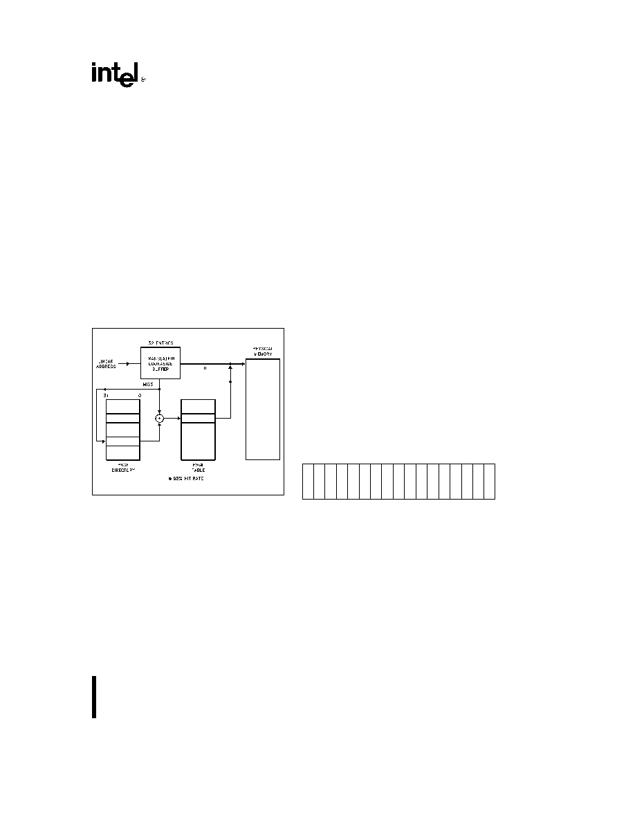
Intel386
TM
DX MICROPROCESSOR
4 5 4 Translation Lookaside Buffer
The Intel386 DX paging hardware is designed to
support demand paged virtual memory systems
However performance would degrade substantially
if the processor was required to access two levels of
tables for every memory reference To solve this
problem the Intel386 DX keeps a cache of the most
recently accessed pages this cache is called the
Translation Lookaside Buffer (TLB) The TLB is a
four-way set associative 32-entry page table cache
It automatically keeps the most commonly used
Page Table Entries in the processor The 32-entry
TLB coupled with a 4K page size results in cover-
age of 128K bytes of memory addresses For many
common multi-tasking systems the TLB will have a
hit rate of about 98% This means that the proces-
sor will only have to access the two-level page struc-
ture on 2% of all memory references Figure 4-22
illustrates how the TLB complements the Intel386
DX's paging mechanism
4 5 5 Paging Operation
231630 � 68
Figure 4-22 Translation Lookaside Buffer
The paging hardware operates in the following fash-
ion The paging unit hardware receives a 32-bit lin-
ear address from the segmentation unit The upper
20 linear address bits are compared with all 32 en-
tries in the TLB to determine if there is a match If
there is a match (i e a TLB hit) then the 32-bit phys-
ical address is calculated and will be placed on the
address bus
However if the page table entry is not in the TLB
the Intel386 DX will read the appropriate Page Direc-
tory Entry If P e 1 on the Page Directory Entry indi-
cating that the page table is in memory then the
Intel386 DX will read the appropriate Page Table En-
try and set the Access bit If P e 1 on the Page
Table Entry indicating that the page is in memory
the Intel386 DX will update the Access and Dirty bits
as needed and fetch the operand The upper 20 bits
of the linear address read from the page table will
be stored in the TLB for future accesses However if
P e 0 for either the Page Directory Entry or the
Page Table Entry then the processor will generate a
page fault an Exception 14
The processor will also generate an exception 14
page fault if the memory reference violated the
page protection attributes (i e U S or R W) (e g try-
ing to write to a read-only page) CR2 will hold the
linear address which caused the page fault If a sec-
ond page fault occurs while the processor is at-
tempting to enter the service routine for the first
then the processor will invoke the page fault (excep-
tion 14) handler a second time rather than the dou-
ble fault (exception 8) handler Since Exception 14 is
classified as a fault CS EIP will point to the instruc-
tion causing the page fault The 16-bit error code
pushed as part of the page fault handler will contain
status bits which indicate the cause of the page
fault
The 16-bit error code is used by the operating sys-
tem to determine how to handle the page fault Fig-
ure 4-23A shows the format of the page-fault error
code and the interpretation of the bits
NOTE
Even though the bits in the error code (U S W R
and P) have similar names as the bits in the Page
Directory Table Entries the interpretation of the er-
ror code bits is different Figure 4-23B indicates
what type of access caused the page fault
15
3 2 1 0
U
U U U U U U U U U U U U U U
W P
S R
Figure 4-23A Page Fault Error Code Format
U S
The U S bit indicates whether the access
causing the fault occurred when the processor was
executing in User Mode (U S e 1) or in Supervisor
mode (U S e 0)
W R
The W R bit indicates whether the access
causing the fault was a Read (W R e 0) or a Write
(W R e 1)
P
The P bit indicates whether a page fault was
caused by a not-present page (P e 0) or by a page
level protection violation (P e 1)
U
UNDEFINED
55

Intel386
TM
DX MICROPROCESSOR
U S
W R
Access Type
0
0
Supervisor Read
0
1
Supervisor Write
1
0
User Read
1
1
User Write
Descriptor table access will fault with U S e 0 even if the program
is executing at level 3
Figure 4-23B Type of Access
Causing Page Fault
4 5 6 Operating System
Responsibilities
The Intel386 DX takes care of the page address
translation process relieving the burden from an op-
erating system in a demand-paged system The op-
erating system is responsible for setting up the initial
page tables and handling any page faults The oper-
ating system also is required to invalidate (i e flush)
the TLB when any changes are made to any of the
page table entries The operating system must re-
load CR3 to cause the TLB to be flushed
Setting up the tables is simply a matter of loading
CR3 with the address of the Page Directory and
allocating space for the Page Directory and the
Page Tables The primary responsibility of the oper-
ating system is to implement a swapping policy and
handle all of the page faults
A final concern of the operating system is to ensure
that the TLB cache matches the information in the
paging tables In particular any time the operating
system sets the P present bit of page table entry to
zero the TLB must be flushed Operating systems
may want to take advantage of the fact that CR3 is
stored as part of a TSS to give every task or group
of tasks its own set of page tables
4 6 VIRTUAL 8086 ENVIRONMENT
4 6 1 Executing 8086 Programs
The Intel386 DX allows the execution of 8086 appli-
cation programs in both Real Mode and in the Virtual
8086 Mode (Virtual Mode) Of the two methods Vir-
tual 8086 Mode offers the system designer the most
flexibility The Virtual 8086 Mode allows the execu-
tion of 8086 applications while still allowing the sys-
tem designer to take full advantage of the Intel386
DX protection mechanism In particular the Intel386
DX allows the simultaneous execution of 8086 oper-
ating systems and its applications and an Intel386
DX operating system and both 80286 and Intel386
DX applications Thus in a multi-user Intel386 DX
computer one person could be running an MS-DOS
spreadsheet another person using MS-DOS and a
third person could be running multiple Unix utilities
and applications Each person in this scenario would
believe that he had the computer completely to him-
self Figure 4-24 illustrates this concept
4 6 2 Virtual 8086 Mode Addressing
Mechanism
One of the major differences between Intel386 DX
Real and Protected modes is how the segment se-
lectors are interpreted When the processor is exe-
cuting in Virtual 8086 Mode the segment registers
are used in an identical fashion to Real Mode The
contents of the segment register is shifted left 4 bits
and added to the offset to form the segment base
linear address
The Intel386 DX allows the operating system to
specify which programs use the 8086 style address
mechanism
and which programs use Protected
Mode addressing on a per task basis Through the
use of paging the one megabyte address space of
the Virtual Mode task can be mapped to anywhere in
the 4 gigabyte linear address space of the Intel386
DX Like Real Mode Virtual Mode effective address-
es (i e segment offsets) that exceed 64K byte will
cause an exception 13 However these restrictions
should not prove to be important because most
tasks running in Virtual 8086 Mode will simply be
existing 8086 application programs
4 6 3 Paging In Virtual Mode
The paging hardware allows the concurrent running
of multiple Virtual Mode tasks and provides protec-
tion and operating system isolation Although it is
not strictly necessary to have the paging hardware
enabled to run Virtual Mode tasks it is needed in
order to run multiple Virtual Mode tasks or to relo-
cate the address space of a Virtual Mode task to
physical address space greater than one megabyte
The paging hardware allows the 20-bit linear ad-
dress produced by a Virtual Mode program to be
divided into up to 256 pages Each one of the pages
can be located anywhere within the maximum 4 giga-
byte physical address space of the Intel386 DX In
addition since CR3 (the Page Directory Base Regis-
ter) is loaded by a task switch each Virtual Mode
task can use a different mapping scheme to map
pages to different physical locations Finally the
paging hardware allows the sharing of the 8086 op-
56

Intel386
TM
DX MICROPROCESSOR
231630 � 69
Figure 4-24 Virtual 8086 Environment Memory Management
erating system code between multiple 8086 applica-
tions Figure 4-24 shows how the Intel386 DX paging
hardware enables multiple 8086 programs to run un-
der a virtual memory demand paged system
4 6 4 Protection and I O Permission
Bitmap
All Virtual 8086 Mode programs execute at privilege
level 3 the level of least privilege As such Virtual
8086 Mode programs are subject to all of the protec-
tion checks defined in Protected Mode (This is dif-
ferent from Real Mode which implicitly is executing
at privilege level 0 the level of greatest privilege )
Thus an attempt to execute a privileged instruction
when in Virtual 8086 Mode will cause an exception
13 fault
The following are privileged instructions which may
be executed only at Privilege Level 0 Therefore at-
tempting to execute these instructions in Virtual
8086 Mode (or anytime CPL
l
0) causes an excep-
tion 13 fault
LIDT
MOV DRn reg
MOV reg DRn
LGDT
MOV TRn reg
MOV reg TRn
LMSW
MOV CRn reg
MOV reg CRn
CLTS
HLT
Several instructions particularly those applying to
the multitasking model and protection model are
available only in Protected Mode Therefore at-
tempting to execute the following instructions in
Real Mode or in Virtual 8086 Mode generates an
exception 6 fault
LTR
STR
LLDT
SLDT
LAR
VERR
LSL
VERW
ARPL
The instructions which are IOPL-sensitive in Protect-
ed Mode are
IN
STI
OUT
CLI
INS
OUTS
REP INS
REP OUTS
57

Intel386
TM
DX MICROPROCESSOR
In Virtual 8086 Mode a slightly different set of in-
structions are made IOPL-sensitive The following in-
structions are IOPL-sensitive in Virtual 8086 Mode
INT n
STI
PUSHF
CLI
POPF
IRET
The PUSHF POPF and IRET instructions are IOPL-
sensitive in Virtual 8086 Mode only This provision
allows the IF flag (interrupt enable flag) to be virtual-
ized to the Virtual 8086 Mode program The INT n
software interrupt instruction is also IOPL-sensitive
in Virtual 8086 Mode Note however that the INT 3
(opcode 0CCH) INTO and BOUND instructions are
not IOPL-sensitive in Virtual 8086 mode (they aren't
IOPL sensitive in Protected Mode either)
Note that the I O instructions (IN OUT INS OUTS
REP INS and REP OUTS) are not IOPL-sensitive in
Virtual 8086 mode Rather the I O instructions be-
come automatically sensitive to the I O Permission
Bitmap
contained in the Intel386 DX Task State
Segment
The I O Permission Bitmap automatically
used by the Intel386 DX in Virtual 8086 Mode is
illustrated by Figures 4 15a and 4-15b
The I O Permission Bitmap can be viewed as a 0 �
64 Kbit bit string which begins in memory at offset
Bit
Map
Offset in the current TSS Bit
Map
Offset must be
s
DFFFH so the entire bit map and
the byte FFH which follows the bit map are all at
offsets
s
FFFFH from the TSS base The 16-bit
pointer Bit
Map
Offset (15 0) is found in the word
beginning at offset 66H (102 decimal) from the TSS
base as shown in Figure 4-15a
Each bit in the I O Permission Bitmap corresponds
to a single byte-wide I O port as illustrated in Figure
4-15a If a bit is 0 I O to the corresponding byte-
wide port can occur without generating an excep-
tion Otherwise the I O instruction causes an excep-
tion 13 fault Since every byte-wide I O port must be
protectable all bits corresponding to a word-wide or
dword-wide port must be 0 for the word-wide or
dword-wide I O to be permitted If all the referenced
bits are 0 the I O will be allowed If any referenced
bits are 1 the attempted I O will cause an exception
13 fault
Due to the use of a pointer to the base of the I O
Permission Bitmap the bitmap may be located any-
where within the TSS or may be ignored completely
by pointing the Bit
Map
Offset (15 0) beyond the
limit of the TSS segment In the same manner only
a small portion of the 64K I O space need have an
associated map bit by adjusting the TSS limit to
truncate the bitmap This eliminates the commitment
of 8K of memory when a complete bitmap is not
required while allowing the fully general case if
desired
EXAMPLE OF BITMAP FOR I O PORTS 0 � 255
Setting the TSS limit to
bit
Map
Offset a 31
a
1
see note below will allow a 32-byte bit-
map for the I O ports
0 � 255 plus a terminator
byte of all 1's
see note below
This allows the
I O bitmap to control I O Permission to I O port 0 �
255 while causing an exception 13 fault on attempt-
ed I O to any I O port 80256 through 65 565
IMPORTANT IMPLEMENTATION NOTE
Beyond
the last byte of I O mapping information in the I O
Permission Bitmap must be a byte containing all 1's
The byte of all 1's must be within the limit of the
Intel386 DX TSS segment (see Figure 4-15a)
4 6 5 Interrupt Handling
In order to fully support the emulation of an 8086
machine interrupts in Virtual 8086 Mode are han-
dled in a unique fashion When running in Virtual
Mode all interrupts and exceptions involve a privi-
lege change back to the host Intel386 DX operating
system The Intel386 DX operating system deter-
mines if the interrupt comes from a Protected Mode
application or from a Virtual Mode program by exam-
ining the VM bit in the EFLAGS image stored on the
stack
When a Virtual Mode program is interrupted and ex-
ecution passes to the interrupt routine at level 0 the
VM bit is cleared However the VM bit is still set in
the EFLAG image on the stack
The Intel386 DX operating system in turn handles
the exception or interrupt and then returns control to
the 8086 program The Intel386 DX operating sys-
tem may choose to let the 8086 operating system
handle the interrupt or it may emulate the function of
the interrupt handler For example many 8086 oper-
ating system calls are accessed by PUSHing param-
eters on the stack and then executing an INT n in-
struction If the IOPL is set to 0 then all INT n instruc-
tions will be intercepted by the Intel386 DX Micro-
processor operating system The Intel386 DX oper-
ating system could emulate the 8086 operating sys-
tem's call Figure 4-25 shows how the Intel386 DX
operating system could intercept an 8086 operating
system's call to ``Open a File''
An Intel386 DX operating system can provide a Vir-
tual 8086 Environment which is totally transparent to
the application software via intercepting and then
emulating 8086 operating system's calls and inter-
cepting IN and OUT instructions
58

Intel386
TM
DX MICROPROCESSOR
4 6 6 Entering and Leaving Virtual
8086 Mode
Virtual 8086 mode is entered by executing an IRET
instruction (at CPLe0) or Task Switch (at any CPL)
to an Intel386 DX task whose Intel386 DX TSS has a
FLAGS image containing a 1 in the VM bit position
while the processor is executing in Protected Mode
That is one way to enter Virtual 8086 mode is to
switch to a task with an Intel386 DX TSS that has a
1 in the VM bit in the EFLAGS image The other way
is to execute a 32-bit IRET instruction at privilege
level 0 where the stack has a 1 in the VM bit in the
EFLAGS image POPF does not affect the VM bit
even if the processor is in Protected Mode or level 0
and so cannot be used to enter Virtual 8086 Mode
PUSHF always pushes a 0 in the VM bit even if the
processor is in Virtual 8086 Mode so that a program
cannot tell if it is executing in REAL mode or in Vir-
tual 8086 mode
The VM bit can be set by executing an IRET instruc-
tion only at privilege level 0 or by any instruction or
Interrupt which causes a task switch in Protected
Mode (with VMe1 in the new FLAGS image) and
can be cleared only by an interrupt or exception in
Virtual 8086 Mode IRET and POPF instructions exe-
cuted in REAL mode or Virtual 8086 mode will not
change the value in the VM bit
The transition out of virtual 8086 mode to Intel386
DX protected mode occurs only on receipt of an in-
terrupt or exception (such as due to a sensitive in-
struction) In Virtual 8086 mode all interrupts and
exceptions vector through the protected mode IDT
and enter an interrupt handler in protected Intel386
DX mode That is as part of interrupt processing
the VM bit is cleared
Because the matching IRET must occur from level 0
if an Interrupt or Trap Gate is used to field an inter-
rupt or exception out of Virtual 8086 mode the Gate
must perform an inter-level interrupt only to level 0
Interrupt or Trap Gates through conforming seg-
ments or through segments with DPL
l
0 will raise a
GP fault with the CS selector as the error code
4 6 6 1 TASK SWITCHES TO FROM VIRTUAL
8086 MODE
Tasks which can execute in virtual 8086 mode must
be described by a TSS with the new Intel386 DX
format (TYPE 9 or 11 descriptor)
A task switch out of virtual 8086 mode will operate
exactly the same as any other task switch out of a
task with an Intel386 DX TSS All of the programmer
visible state including the FLAGS register with the
VM bit set to 1 is stored in the TSS The segment
registers in the TSS will contain 8086 segment base
values rather than selectors
A task switch into a task described by an Intel386
DX TSS will have an additional check to determine if
the incoming task should be resumed in virtual 8086
mode Tasks described by 80286 format TSSs can-
not be resumed in virtual 8086 mode so no check is
required there (the FLAGS image in 80286 format
TSS has only the low order 16 FLAGS bits) Before
loading the segment register images from an In-
tel386 DX TSS the FLAGS image is loaded so that
the segment registers are loaded from the TSS im-
age as 8086 segment base values The task is now
ready to resume in virtual 8086 execution mode
4 6 6 2 TRANSITIONS THROUGH TRAP AND
INTERRUPT GATES AND IRET
A task switch is one way to enter or exit virtual 8086
mode The other method is to exit through a Trap or
Interrupt gate as part of handling an interrupt and
to enter as part of executing an IRET instruction
The transition out must use an Intel386 DX Trap
Gate (Type 14) or Intel386 DX Interrupt Gate (Type
15) which must point to a non-conforming level 0
segment (DPLe0) in order to permit the trap han-
dler to IRET back to the Virtual 8086 program The
Gate must point to a non-conforming level 0 seg-
ment to perform a level switch to level 0 so that the
matching IRET can change the VM bit Intel386 DX
gates must be used since 80286 gates save only
the low 16 bits of the FLAGS register so that the VM
bit will not be saved on transitions through the
80286 gates Also the 16-bit IRET (presumably)
used to terminate the 80286 interrupt handler will
pop only the lower 16 bits from FLAGS and will not
affect the VM bit The action taken for an Intel386
DX Trap or Interrupt gate if an interrupt occurs while
the task is executing in virtual 8086 mode is given by
the following sequence
(1) Save the FLAGS register in a temp to push later
Turn off the VM and TF bits and if the interrupt is
serviced by an Interrupt Gate turn off IF also
(2) Interrupt and Trap gates must perform a level
switch from 3 (where the VM86 program exe-
cutes) to level 0 (so IRET can return) This pro-
cess involves a stack switch to the stack given in
the TSS for privilege level 0 Save the Virtual
8086 Mode SS and ESP registers to push in a
later step The segment register load of SS will
be done as a Protected Mode segment load
since the VM bit was turned off above
(3) Push the 8086 segment register values onto the
new stack in the order GS FS DS ES These
are pushed as 32-bit quantities with undefined
values in the upper 16 bits Then load these 4
registers with null selectors (0)
59

Intel386
TM
DX MICROPROCESSOR
8086 Application makes ``Open File Call''
x
causes
231630 � 70
General Protection Fault (Arrow
1)
Virtual 8086 Monitor intercepts call Calls Intel386
TM
DX OS (Arrow
2)
Intel386
TM
DX OS opens file returns control to 8086 OS (Arrow
3)
8086 OS returns control to application (Arrow
4)
Transparent to Application
Figure 4-25 Virtual 8086 Environment Interrupt and Call Handling
(4) Push the old 8086 stack pointer onto the new
stack by pushing the SS register (as 32-bits high
bits undefined) then pushing the 32-bit ESP reg-
ister saved above
(5) Push the 32-bit FLAGS register saved in step 1
(6) Push the old 8086 instruction pointer onto the
new stack by pushing the CS register (as 32-bits
high bits undefined) then pushing the 32-bit EIP
register
(7) Load up the new CS EIP value from the interrupt
gate and begin execution of the interrupt routine
in protected Intel386 DX mode
The transition out of virtual 8086 mode performs a
level change and stack switch in addition to chang-
ing back to protected mode In addition all of the
8086 segment register images are stored on the
stack (behind the SS ESP image) and then loaded
with null (0) selectors before entering the interrupt
handler This will permit the handler to safely save
and restore the DS ES FS and GS registers as
80286 selectors This is needed so that interrupt
handlers which don't care about the mode of the
interrupted program can use the same prolog and
epilog code for state saving (i e push all registers in
prolog pop all in epilog) regardless of whether or not
a ``native'' mode or Virtual 8086 mode program was
interrupted Restoring null selectors to these regis-
ters before executing the IRET will not cause a trap
in the interrupt handler Interrupt routines which ex-
pect values in the segment registers or return val-
ues in segment registers will have to obtain return
values from the 8086 register images pushed onto
the new stack They will need to know the mode of
the interrupted program in order to know where to
find return segment registers and also to know how
to interpret segment register values
The IRET instruction will perform the inverse of the
above sequence Only the extended Intel386 DXs
IRET instruction (operand sizee32) can be used
and must be executed at level 0 to change the VM
bit to 1
(1) If the NT bit in the FLAGs register is on an inter-
task return is performed The current state is
stored in the current TSS and the link field in the
current TSS is used to locate the TSS for the
interrupted task which is to be resumed
Otherwise continue with the following sequence
(2) Read the FLAGS image from SS 8 ESP into the
FLAGS register This will set VM to the value ac-
tive in the interrupted routine
(3) Pop off the instruction pointer CS EIP EIP is
popped first then a 32-bit word is popped which
contains the CS value in the lower 16 bits If
VMe0 this CS load is done as a protected
mode segment load If VMe1 this will be done
as an 8086 segment load
(4) Increment the ESP register by 4 to bypass the
FLAGS image which was ``popped'' in step 1
(5) If VMe1 load segment registers ES DS FS
and GS from memory locations SS ESPa8
SS ESPa12
SS ESPa16
and
SS ESPa20
respectively where the new val-
60

Intel386
TM
DX MICROPROCESSOR
ue of ESP stored in step 4 is used Since VMe1
these are done as 8086 segment register loads
Else if VMe0 check that the selectors in ES
DS FS and GS are valid in the interrupted rou-
tine Null out invalid selectors to trap if an at-
tempt is made to access through them
(6) If (RPL(CS)
l
CPL)
pop the stack pointer
SS ESP from the stack The ESP register is
popped first followed by 32-bits containing SS in
the lower 16 bits If VMe0 SS is loaded as a
protected mode segment register load If VMe1
an 8086 segment register load is used
(7) Resume execution of the interrupted routine The
VM bit in the FLAGS register (restored from the
interrupt routine's stack image in step 1) deter-
mines whether the processor resumes the inter-
rupted routine in Protected mode of Virtual 8086
mode
5 FUNCTIONAL DATA
5 1 INTRODUCTION
The Intel386 DX features a straightforward function-
al interface to the external hardware The Intel386
DX has separate parallel buses for data and ad-
dress The data bus is 32-bits in width and bidirec-
tional The address bus outputs 32-bit address val-
ues in the most directly usable form for the high-
speed local bus 4 individual byte enable signals
and the 30 upper-order bits as a binary value The
data and address buses are interpreted and con-
trolled with their associated control signals
A dynamic data bus sizing feature allows the proc-
essor to handle a mix of 32- and 16-bit external bus-
es on a cycle-by-cycle basis (see 5 3 4 Data Bus
Sizing
) If 16-bit bus size is selected the Intel386
DX automatically makes any adjustment needed
even performing another 16-bit bus cycle to com-
plete the transfer if that is necessary 8-bit peripheral
devices may be connected to 32-bit or 16-bit buses
with no loss of performance A new address pipe-
lining option
is provided and applies to 32-bit and
16-bit buses for substantially improved memory utili-
zation especially for the most heavily used memory
resources
The address pipelining option when selected typ-
ically allows a given memory interface to operate
with one less wait state than would otherwise be
required (see 5 4 2 Address Pipelining) The pipe-
lined bus is also well suited to interleaved memory
designs When address pipelining is requested by
the external hardware the Intel386 DX will output
the address and bus cycle definition of the next bus
cycle (if it is internally available) even while waiting
for the current cycle to be acknowledged
Non-pipelined address timing however is ideal for
external cache designs since the cache memory will
typically be fast enough to allow non-pipelined cy-
cles For maximum design flexibility the address
pipelining option is selectable on a cycle-by-cycle
basis
The processor's bus cycle is the basic mechanism
for information transfer either from system to proc-
essor or from processor to system Intel386 DX bus
cycles perform data transfer in a minimum of only
two clock periods On a 32-bit data bus the maxi-
mum Intel386 DX transfer bandwidth at 20 MHz is
therefore 40 MBytes sec at 25 MHz bandwidth is
50 Mbytes sec
and at 33 MHz bandwidth
is
66 Mbytes sec Any bus cycle will be extended for
more than two clock periods however if external
hardware withholds acknowledgement of the cycle
At the appropriate time acknowledgement is sig-
nalled by asserting the Intel386 DX READY
input
The Intel386 DX can relinquish control of its local
buses to allow mastership by other devices such as
direct memory access channels When relinquished
HLDA is the only output pin driven by the Intel386
DX providing near-complete isolation of the proces-
sor from its system The near-complete isolation
characteristic is ideal when driving the system from
test equipment and in fault-tolerant applications
Functional data covered in this chapter describes
the processor's hardware interface First the set of
signals available at the processor pins is described
(see 5 2 Signal Description) Following that are the
signal waveforms occurring during bus cycles (see
5 3 Bus Transfer Mechanism 5 4 Bus Functional
Description
and 5 5 Other Functional Descrip-
tions
)
5 2 SIGNAL DESCRIPTION
5 2 1 Introduction
Ahead is a brief description of the Intel386 DX input
and output signals arranged by functional groups
Note the
symbol at the end of a signal name indi-
cates the active or asserted state occurs when the
signal is at a low voltage When no
is present after
the signal name the signal is asserted when at the
high voltage level
Example signal M IO
High voltage indicates
Memory selected
Low
voltage
indicates
I O selected
61

Intel386
TM
DX MICROPROCESSOR
231630 � 1
Figure 5-1 Functional Signal Groups
231630 � 2
Figure 5-2 CLK2 Signal and Internal Processor Clock
The signal descriptions sometimes refer to AC tim-
ing parameters such as ``t
25
Reset Setup Time'' and
``t
26
Reset Hold Time '' The values of these parame-
ters can be found in Tables 7-4 and 7-5
5 2 2 Clock (CLK2)
CLK2 provides the fundamental timing for the In-
tel386 DX It is divided by two internally to generate
the internal processor clock used for instruction exe-
cution The internal clock is comprised of two phas-
es ``phase one'' and ``phase two '' Each CLK2 peri-
od is a phase of the internal clock Figure 5-2 illus-
trates the relationship If desired the phase of the
internal processor clock can be synchronized to a
known phase by ensuring the RESET signal falling
edge meets its applicable setup and hold times t
25
and t
26
5 2 3 Data Bus (D0 through D31)
These three-state bidirectional signals provide the
general purpose data path between the Intel386 DX
and other devices Data bus inputs and outputs indi-
cate ``1'' when HIGH The data bus can transfer data
on 32- and 16-bit buses using a data bus sizing fea-
ture controlled by the BS16
input See section
5 2 6 Bus Contol
Data bus reads require that read
data setup and hold times t
21
and t
22
be met for
correct operation In addition the Intel386 DX re-
quires that all data bus pins be at a valid logic state
(high or low) at the end of each read cycle when
READY
is asserted During any write operation
(and during halt cycles and shutdown cycles) the
Intel386 DX always drives all 32 signals of the data
bus even if the current bus size is 16-bits
5 2 4 Address Bus (BE0
through
BE3
A2 through A31)
These three-state outputs provide physical memory
addresses or I O port addresses The address bus
is capable of addressing 4 gigabytes of physical
memory space (00000000H through FFFFFFFFH)
and 64 kilobytes of I O address space (00000000H
through 0000FFFFH) for programmed I O
I O
62

Intel386
TM
DX MICROPROCESSOR
transfers automatically generated for Intel386 DX-to-
coprocessor communication use I O addresses
800000F8H through 800000FFH so A31 HIGH in
conjunction with M IO
LOW allows simple genera-
tion of the coprocessor select signal
The Byte Enable outputs BE0
� BE3
directly in-
dicate which bytes of the 32-bit data bus are in-
volved with the current transfer This is most conve-
nient for external hardware
BE0
applies to D0 � D7
BE1
applies to D8 � D15
BE2
applies to D16 � D23
BE3
applies to D24 � D31
The number of Byte Enables asserted indicates the
physical size of the operand being transferred (1 2
3 or 4 bytes) Refer to section 5 3 6 Operand Align-
ment
When a memory write cycle or I O write cycle is in
progress and the operand being transferred occu-
pies only the upper 16 bits of the data bus (D16 �
D31) duplicate data is simultaneously presented on
the corresponding lower 16-bits of the data bus
(D0 � D15) This duplication is performed for optimum
write performance on 16-bit buses The pattern of
write data duplication is a function of the Byte En-
ables asserted during the write cycle Table 5-1 lists
the write data present on D0 � D31 as a function of
the asserted Byte Enable outputs BE0
� BE3
5 2 5 Bus Cycle Definition Signals
(W R
D C
M IO
LOCK )
These three-state outputs define the type of bus cy-
cle being performed W R
distinguishes between
write and read cycles D C
distinguishes between
data and control cycles M IO
distinguishes be-
tween memory and I O cycles
LOCK
distin-
guishes between locked and unlocked bus cycles
The primary bus cycle definition signals are W R
D C
and M IO
since these are the signals driv-
en valid as the ADS
(Address Status output) is
driven asserted The LOCK
is driven valid at the
same time as the first locked bus cycle begins
which due to address pipelining could be later than
ADS
is driven asserted See 5 4 3 4 Pipelined Ad-
dress
The LOCK
is negated when the READY
input terminates the last bus cycle which was
locked
Exact bus cycle definitions as a function of W R
D C
and M IO
are given in Table 5-2 Note one
combination of W R
D C
and M IO
is never
given when ADS
is asserted (however that combi-
nation which is listed as ``does not occur '' may oc-
cur during idle bus states when ADS
is not assert-
ed) If M IO
D C
and W R
are qualified by
ADS
asserted then a decoding scheme may be
simplified by using this definition of the ``does not
occur'' combination
Table 5-1 Write Data Duplication as a Function of BE0
� BE3
Intel386
TM
DX Byte Enables
Intel386
TM
DX Write Data
Automatic
BE3
BE2
BE1
BE0
D24 � D31
D16 � D23
D8 � D15
D0 � D7
Duplication
High
High
High
Low
undef
undef
undef
A
No
High
High
Low
High
undef
undef
B
undef
No
High
Low
High
High
undef
C
undef
C
Yes
Low
High
High
High
D
undef
D
undef
Yes
High
High
Low
Low
undef
undef
B
A
No
High
Low
Low
High
undef
C
B
undef
No
Low
Low
High
High
D
C
D
C
Yes
High
Low
Low
Low
undef
C
B
A
No
Low
Low
Low
High
D
C
B
undef
No
Low
Low
Low
Low
D
C
B
A
No
Key
D e logical write data d24 � d31
C e logical write data d16 � d23
B e logical write data d8 � d15
A e logical write data d0 � d7
63

Intel386
TM
DX MICROPROCESSOR
Table 5-2 Bus Cycle Definition
M IO
D C
W R
Bus Cycle Type
Locked
Low
Low
Low
INTERRUPT ACKNOWLEDGE
Yes
Low
Low
High
does not occur
Low
High
Low
I O DATA READ
No
Low
High
High
I O DATA WRITE
No
High
Low
Low
MEMORY CODE READ
No
High
Low
High
HALT
SHUTDOWN
No
Address e 2
Address e 0
(BE0
High
(BE0
Low
BE1
High
BE1
High
BE2
Low
BE2
High
BE3
High
BE3
High
A2 � A31 Low)
A2 � A31 Low)
High
High
Low
MEMORY DATA READ
Some Cycles
High
High
High
MEMORY DATA WRITE
Some Cycles
5 2 6 Bus Control Signals (ADS
READY
NA
BS16 )
5 2 6 1 INTRODUCTION
The following signals allow the processor to indicate
when a bus cycle has begun and allow other system
hardware to control address pipelining data bus
width and bus cycle termination
5 2 6 2 ADDRESS STATUS (ADS )
This three-state output indicates that a valid bus cy-
cle definition and address (W R
D C
M IO
BE0
� BE3
and A2 � A31) is being driven at the
Intel386 DX pins It is asserted during T1 and T2P
bus states (see 5 4 3 2 Non-pipelined Address and
5 4 3 4 Pipelined Address
for additional information
on bus states)
5 2 6 3 TRANSFER ACKNOWLEDGE (READY )
This input indicates the current bus cycle is com-
plete and the active bytes indicated by BE0
�
BE3
and BS16
are accepted or provided When
READY
is sampled asserted during a read cycle or
interrupt acknowledge cycle the Intel386 DX latches
the input data and terminates the cycle When
READY
is sampled asserted during a write cycle
the processor terminates the bus cycle
READY
is ignored on the first bus state of all bus
cycles and sampled each bus state thereafter until
asserted READY
must eventually be asserted to
acknowledge every bus cycle including Halt Indica-
tion and Shutdown Indication bus cycles When be-
ing sampled READY must always meet setup and
hold times t
19
and t
20
for correct operation See all
sections of 5 4 Bus Functional Description
5 2 6 4 NEXT ADDRESS REQUEST (NA )
This is used to request address pipelining This input
indicates the system is prepared to accept new val-
ues of BE0
� BE3
A2 � A31 W R
D C
and
M IO
from the Intel386 DX even if the end of the
current
cycle
is
not
being
acknowledged
on
READY
If this input is asserted when sampled
the next address is driven onto the bus provided the
next bus request is already pending internally See
5 4 2 Address Pipelining
and 5 4 3 Read and
Write Cycles
NA
must always meet setup and
hold times t
15
and t
16
for correct operation
5 2 6 5 BUS SIZE 16 (BS16 )
The BS16
feature allows the Intel386 DX to direct-
ly connect to 32-bit and 16-bit data buses Asserting
this input constrains the current bus cycle to use
only the lower-order half (D0 � D15) of the data bus
corresponding to BE0
and BE1
Asserting
BS16
has no additional effect if only BE0
and or
BE1
are asserted in the current cycle However
during bus cycles asserting BE2
or BE3
assert-
ing BS16
will automatically cause the Intel386 DX
to make adjustments for correct transfer of the up-
per bytes(s) using only physical data signals D0 �
D15
If the operand spans both halves of the data bus
and BS16
is asserted the Intel386 DX will auto-
matically perform another 16-bit bus cycle BS16
must always meet setup and hold times t
17
and t
18
for correct operation
64

Intel386
TM
DX MICROPROCESSOR
Intel386 DX I O cycles are automatically generated
for coprocessor communication Since the Intel386
DX must transfer 32-bit quantities between itself and
the Intel387 DX BS16
must not
be asserted dur-
ing Intel387 DX communication cycles
5 2 7 Bus Arbitration Signals
(HOLD HLDA)
5 2 7 1 INTRODUCTION
This section describes the mechanism by which the
processor relinquishes control of its local buses
when requested by another bus master device See
5 5 1 Entering and Exiting Hold Acknowledge
for
additional information
5 2 7 2 BUS HOLD REQUEST (HOLD)
This input indicates some device other than the In-
tel386 DX requires bus mastership
HOLD must remain asserted as long as any other
device is a local bus master HOLD is not recognized
while RESET is asserted If RESET is asserted while
HOLD is asserted RESET has priority and places
the bus into an idle state rather than the hold ac-
knowledge (high impedance) state
HOLD is level-sensitive and is a synchronous input
HOLD signals must always meet setup and hold
times t
23
and t
24
for correct operation
5 2 7 3 BUS HOLD ACKNOWLEDGE (HLDA)
Assertion of this output indicates the Intel386 DX
has relinquished control of its local bus in response
to HOLD asserted and is in the bus Hold Acknowl-
edge state
The Hold Acknowledge state offers near-complete
signal isolation In the Hold Acknowledge state
HLDA is the only signal being driven by the Intel386
DX The other output signals or bidirectional signals
(D0 � D31 BE0
� BE3
A2 � A31 W R
D C
M IO
LOCK
and ADS ) are in a high-imped-
ance state so the requesting bus master may control
them Pullup resistors may be desired on several sig-
nals to avoid spurious activity when no bus master is
driving them See 7 2 3 Resistor Recommenda-
tions
Also one rising edge occuring on the NMI
input during Hold Acknowledge is remembered for
processing after the HOLD input is negated
In addition to the normal usage of Hold Acknowl-
edge with DMA controllers or master peripherals
the near-complete isolation has particular attractive-
ness during system test when test equipment drives
the system and in hardware-fault-tolerant applica-
tions
5 2 8 Coprocessor Interface Signals
(PEREQ BUSY
ERROR )
5 2 8 1 INTRODUCTION
In the following sections are descriptions of signals
dedicated to the numeric coprocessor interface In
addition to the data bus address bus and bus cycle
definition signals these following signals control
communication between the Intel386 DX and its In-
tel387 DX processor extension
5 2 8 2 COPROCESSOR REQUEST (PEREQ)
When asserted this input signal indicates a coproc-
essor request for a data operand to be transferred
to from memory by the Intel386 DX In response
the Intel386 DX transfers information between the
coprocessor and memory Because the Intel386 DX
has internally stored the coprocessor opcode being
executed it performs the requested data transfer
with the correct direction and memory address
PEREQ is level-sensitive and is allowed to be asyn-
chronous to the CLK2 signal
5 2 8 3 COPROCESSOR BUSY (BUSY )
When asserted this input indicates the coprocessor
is still executing an instruction and is not yet able to
accept another When the Intel386 DX encounters
any coprocessor instruction which operates on the
numeric stack (e g load pop or arithmetic opera-
tion) or the WAIT instruction this input is first auto-
matically sampled until it is seen to be negated This
sampling of the BUSY
input prevents overrunning
the execution of a previous coprocessor instruction
The FNINIT and FNCLEX coprocessor instructions
are allowed to execute even if BUSY
is asserted
since these instructions are used for coprocessor
initialization and exception-clearing
BUSY
is level-sensitive and is allowed to be asyn-
chronous to the CLK2 signal
BUSY
serves an additional function If BUSY
is
sampled LOW at the falling edge of RESET the In-
tel386 DX performs an internal self-test (see 5 5 3
Bus Activity During and Following Reset
)
If
BUSY
is sampled HIGH no self-test is performed
65

Intel386
TM
DX MICROPROCESSOR
5 2 8 4 COPROCESSOR ERROR (ERROR )
This input signal indicates that the previous coproc-
essor instruction generated a coprocessor error of a
type not masked by the coprocessor's control regis-
ter This input is automatically sampled by the In-
tel386 DX when a coprocessor instruction is en-
countered and if asserted the Intel386 DX gener-
ates exception 16 to access the error-handling soft-
ware
Several coprocessor instructions generally those
which clear the numeric error flags in the coproces-
sor or save coprocessor state do execute without
the Intel386 DX generating exception 16 even if ER-
ROR
is asserted These instructions are FNINIT
FNCLEX FSTSW FSTSWAX FSTCW FSTENV
FSAVE FESTENV and FESAVE
ERROR
is level-sensitive and is allowed to be
asynchronous to the CLK2 signal
5 2 9 Interrupt Signals (INTR NMI
RESET)
5 2 9 1 INTRODUCTION
The following descriptions cover inputs that can in-
terrupt or suspend execution of the processor's cur-
rent instruction stream
5 2 9 2 MASKABLE INTERRUPT REQUEST (INTR)
When asserted this input indicates a request for in-
terrupt service which can be masked by the Intel386
DX Flag Register IF bit When the Intel386 DX re-
sponds to the INTR input it performs two interrupt
acknowledge bus cycles and at the end of the sec-
ond latches an 8-bit interrupt vector on D0 � D7 to
identify the source of the interrupt
INTR is level-sensitive and is allowed to be asyn-
chronous to the CLK2 signal To assure recognition
of an INTR request INTR should remain asserted
until the first interrupt acknowledge bus cycle be-
gins
5 2 9 3 NON-MASKABLE INTERRUPT REQUEST
(NMI)
This input indicates a request for interrupt service
which cannot be masked by software The non-
maskable interrupt request is always processed ac-
cording to the pointer or gate in slot 2 of the interrupt
table Because of the fixed NMI slot assignment no
interrupt acknowledge cycles are perfomed when
processing NMI
NMI is rising edge-sensitive and is allowed to be
asynchronous to the CLK2 signal To assure recog-
nition of NMI it must be negated for at least eight
CLK2 periods and then be asserted for at least
eight CLK2 periods
Once NMI processing has begun
no additional
NMI's are processed until after the next IRET in-
struction which is typically the end of the NMI serv-
ice routine If NMI is re-asserted prior to that time
however one rising edge on NMI will be remem-
bered for processing after executing the next IRET
instruction
5 2 9 4 RESET (RESET)
This input signal suspends any operation in progress
and places the Intel386 DX in a known reset state
The Intel386 DX is reset by asserting RESET for 15
or more CLK2 periods (80 or more CLK2 periods
before requesting self test) When RESET is assert-
ed all other input pins are ignored and all other bus
pins are driven to an idle bus state as shown in Ta-
ble 5-3 If RESET and HOLD are both asserted at a
point in time RESET takes priority even if the In-
tel386 DX was in a Hold Acknowledge state prior to
RESET asserted
RESET is level-sensitive and must be synchronous
to the CLK2 signal If desired the phase of the inter-
nal processor clock and the entire Intel386 DX state
can be completely synchronized to external circuitry
by ensuring the RESET signal falling edge meets its
applicable setup and hold times t
25
and t
26
Table 5-3 Pin State (Bus Idle) During Reset
Pin Name
Signal Level During Reset
ADS
High
D0�D31
High Impedance
BE0
�BE3
Low
A2�A31
High
W R
Low
D C
High
M IO
Low
LOCK
High
HLDA
Low
66

Intel386
TM
DX MICROPROCESSOR
5 2 10 Signal Summary
Table 5-4 summarizes the characteristics of all Intel386 DX signals
Table 5-4 Intel386
TM
DX Signal Summary
Input
Output
Signal Name
Signal Function
Active
Input
Synch or
High Impedance
State
Output
Asynch
During HLDA
to CLK2
CLK2
Clock
I
D0 � D31
Data Bus
High
I O
S
Yes
BE0
� BE3
Byte Enables
Low
O
Yes
A2 � A31
Address Bus
High
O
Yes
W R
Write-Read Indication
High
O
Yes
D C
Data-Control Indication
High
O
Yes
M IO
Memory-I O Indication
High
O
Yes
LOCK
Bus Lock Indication
Low
O
Yes
ADS
Address Status
Low
O
Yes
NA
Next Address Request
Low
I
S
BS16
Bus Size 16
Low
I
S
READY
Transfer Acknowledge
Low
I
S
HOLD
Bus Hold Request
High
I
S
HLDA
Bus Hold Acknowledge
High
O
No
PEREQ
Coprocessor Request
High
I
A
BUSY
Coprocessor Busy
Low
I
A
ERROR
Coprocessor Error
Low
I
A
INTR
Maskable Interrupt Request
High
I
A
NMI
Non-Maskable Intrpt Request
High
I
A
RESET
Reset
High
I
S
5 3 BUS TRANSFER MECHANISM
5 3 1 Introduction
All data transfers occur as a result of one or more
bus cycles Logical data operands of byte word and
double-word lengths may be transferred without re-
strictions on physical address alignment Any byte
boundary may be used although two or even three
physical bus cycles are performed as required for
unaligned operand transfers See 5 3 4 Dynamic
Data Bus Sizing
and 5 3 6 Operand Alignment
The Intel386 DX address signals are designed to
simplify external system hardware Higher-order ad-
dress bits are provided by A2 � A31 Lower-order ad-
dress in the form of BE0
� BE3
directly provides
linear selects for the four bytes of the 32-bit data
bus Physical operand size information is thereby im-
plicitly provided each bus cycle in the most usable
form
Byte Enable outputs BE0
� BE3
are asserted
when their associated data bus bytes are involved
with the present bus cycle as listed in Table 5-5
During a bus cycle any possible pattern of contigu-
ous asserted Byte Enable outputs can occur but
never patterns having a negated Byte Enable sepa-
rating two or three asserted Enables
67

Intel386
TM
DX MICROPROCESSOR
Address bits A0 and A1 of the physical operand's
base address can be created when necessary (for
instance for MULTIBUS I or MULTIBUS II interface)
as a function of the lowest-order asserted Byte En-
able This is shown by Table 5-6 Logic to generate
A0 and A1 is given by Figure 5-3
Table 5-5 Byte Enables and Associated
Data and Operand Bytes
Byte Enable Signal
Associated Data Bus Signals
BE0
D0 � D7
(byte 0
least significant)
BE1
D8 � D15
(byte 1)
BE2
D16 � D23 (byte 2)
BE3
D24 � D31 (byte 3
most significant)
Table 5-6 Generating A0 � A31 from
BE0
� BE3
and A2 � A31
Intel386
TM
DX Address Signals
A31
A2
BE3
BE2
BE1
BE0
Physical Base
Address
A31
A2 A1 A0
A31
A2 0
0
X
X
X
Low
A31
A2 0
1
X
X
Low
High
A31
A2 1
0
X
Low
High
High
A31
A2 1
1
Low
High
High
High
231630 � 3
K - Map for A1 Signal
231630 � 4
K - Map for A0 Signal
Figure 5-3 Logic to Generate A0 A1 from BE0
� BE3
Each bus cycle is composed of at least two bus
states Each bus state requires one processor clock
period Additional bus states added to a single bus
cycle are called wait states See 5 4 Bus Functional
Description
Since a bus cycle requires a minimum of two bus
states (equal to two processor clock periods) data
can be transferred between external devices and
the Intel386 DX at a maximum rate of one 4-byte
Dword every two processor clock periods for a max-
imum bus bandwidth of 66 megabytes second (In-
tel386 DX operating at 33 MHz processor clock
rate)
5 3 2 Memory and I O Spaces
Bus cycles may access physical memory space or
I O space Peripheral devices in the system may ei-
ther be memory-mapped or I O-mapped or both
As shown in Figure 5-4 physical memory addresses
range from 00000000H to FFFFFFFFH (4 gigabytes)
and I O addresses from 00000000H to 0000FFFFH
(64 kilobytes) for programmed I O Note the I O ad-
dresses used by the automatic I O cycles for co-
processor
communication
are
800000F8H
to
800000FFH
beyond the address range of pro-
grammed I O to allow easy generation of a coproc-
essor chip select signal using the A31 and M IO
signals
68

Intel386
TM
DX MICROPROCESSOR
231630 � 5
Physical Memory Space
I O Space
NOTE
Since A31 is HIGH during automatic communication with coprocessor A31 HIGH and M IO
LOW can be used to
easily generate a coprocessor select signal
Figure 5-4 Physical Memory and I O Spaces
5 3 3 Memory and I O Organization
The Intel386 DX datapath to memory and I O
spaces can be 32 bits wide or 16 bits wide When
32-bits wide memory and I O spaces are organized
naturally as arrays of physical 32-bit Dwords Each
memory or I O Dword has four individually address-
able bytes at consecutive byte addresses The low-
est-addressed byte is associated with data signals
D0 � D7 the highest-addressed byte with D24 � D31
The Intel386 DX includes a bus control input
BS16
that also allows direct connection to 16-bit
memory or I O spaces organized as a sequence of
16-bit words Cycles to 32-bit and 16-bit memory or
I O devices may occur in any sequence since the
BS16
control is sampled during each bus cycle
See 5 3 4 Dynamic Data Bus Sizing The Byte En-
able signals BE0
� BE3
allow byte granularity
when addressing any memory or I O structure
whether 32 or 16 bits wide
5 3 4 Dynamic Data Bus Sizing
Dynamic data bus sizing is a feature allowing direct
processor connection to 32-bit or 16-bit data buses
for memory or I O A single processor may connect
to both size buses Transfers to or from 32- or 16-bit
ports are supported by dynamically determining the
bus width during each bus cycle During each bus
cycle an address decoding circuit or the slave de-
vice itself may assert BS16
for 16-bit ports or ne-
gate BS16
for 32-bit ports
With BS16
asserted the processor automatically
converts operand transfers larger than 16 bits or
misaligned 16-bit transfers into two or three trans-
fers as required All operand transfers physically oc-
cur on D0 � D15 when BS16
is asserted There-
fore 16-bit memories or I O devices only connect
on data signals D0 � D15 No extra transceivers are
required
Asserting BS16
only affects the processor when
BE2
and or BE3
are asserted during the current
cycle If only D0 � D15 are involved with the transfer
asserting BS16
has no affect since the transfer
can proceed normally over a 16-bit bus whether
BS16
is asserted or not In other words asserting
BS16
has no effect when only the lower half of the
bus is involved with the current cycle
There are two types of situations where the proces-
sor is affected by asserting BS16
depending on
which Byte Enables are asserted during the current
bus cycle
Upper Half Only
Only BE2
and or BE3
asserted
Upper and Lower Half
At least BE1
BE2
asserted (and perhaps
also BE0
and or BE3 )
69

Intel386
TM
DX MICROPROCESSOR
Effect of asserting BS16
during ``upper half only''
read cycles
Asserting BS16
during ``upper half only'' reads
causes the Intel386 DX to read data on the lower
16 bits of the data bus and ignore data on the
upper 16 bits of the data bus Data that would
have been read from D16 � D31 (as indicated by
BE2
and BE3 ) will instead be read from D0 �
D15 respectively
Effect of asserting BS16
during ``upper half only''
write cycles
Asserting BS16
during ``upper half only'' writes
does not affect the Intel386 DX When only BE2
and or BE3
are asserted during a write cycle
the Intel386 DX always duplicates data signals
D16 � D31 onto D0 � D15 (see Table 5-1) There-
fore no further Intel386 DX action is required to
perform these writes on 32-bit or 16-bit buses
Effect of asserting BS16
during ``upper and lower
half'' read cycles
Asserting BS16
during ``upper and lower half''
reads causes the processor to perform two 16-bit
read cycles for complete physical operand trans-
fer Bytes 0 and 1 (as indicated by BE0
and
BE1 ) are read on the first cycle using D0 � D15
Bytes 2 and 3 (as indicated by BE2
and BE3 )
are read during the second cycle again using
D0 � D15 D16 � D31 are ignored during both 16-bit
cycles BE0
and BE1
are always negated dur-
ing the second 16-bit cycle (See Figure 5-14 cy-
cles 2 and 2a
)
Effect of asserting BS16
during ``upper and lower
half'' write cycles
Asserting BS16
during ``upper and lower half''
writes causes the Intel386 DX to perform two
16-bit write cycles for complete physical operand
transfer All bytes are available the first write cycle
allowing external hardware to receive Bytes 0 and
1 (as indicated by BE0
and BE1 ) using D0 �
D15 On the second cycle the Intel386 DX dupli-
cates Bytes 2 and 3 on D0 � D15 and Bytes 2 and
3 (as indicated by BE2
and BE3 ) are written
using D0 � D15 BE0
and BE1
are always neg-
ated during the second 16-bit cycle BS16
must
be asserted during the second 16-bit cycle See
Figure 5-14 cycles 1 and 1a
5 3 5 Interfacing with 32- and 16-Bit
Memories
In 32-bit-wide physical memories such as Figure 5-5
each physical Dword begins at a byte address that is
a multiple of 4 A2 � A31 are directly used as a Dword
select and BE0
� BE3
as byte selects BS16
is
negated for all bus cycles involving the 32-bit array
When 16-bit-wide physical arrays are included in the
system as in Figure 5-6 each 16-bit physical word
begins at a address that is a multiple of 2 Note the
address is decoded to assert BS16
only during
bus cycles involving the 16-bit array (If desiring to
231630 � 6
Figure 5-5 Intel386
TM
DX with 32-Bit Memory
231630 � 7
Figure 5-6 Intel386
TM
DX with 32-Bit and 16-Bit Memory
70

Intel386
TM
DX MICROPROCESSOR
use pipelined address with 16-bit memories then
BE0
� BE3
and W R
are also decoded to de-
termine when BS16
should be asserted
See
5 4 3 6 Pipelined Address with Dynamic Data Bus
Sizing
)
A2 � A31 are directly usable for addressing 32-bit
and 16-bit devices To address 16-bit devices A1
and two byte enable signals are also needed
To generate an A1 signal and two Byte Enable sig-
nals for 16-bit access BE0
� BE3
should be de-
coded as in Table 5-7 Note certain combinations of
BE0
� BE3
are never generated by the Intel386
DX leading to ``don't care'' conditions in the decod-
er Any BE0
� BE3
decoder such as Figure 5-7
may use the non-occurring BE0
� BE3
combina-
tions to its best advantage
5 3 6 Operand Alignment
With the flexibility of memory addressing on the In-
tel386 DX it is possible to transfer a logical operand
that spans more than one physical Dword or word of
memory
or
I O
Examples
are
32-bit
Dword
operands beginning at addresses not evenly divisi-
ble by 4 or a 16-bit word operand split between two
physical Dwords of the memory array
Operand alignment and data bus size dictate when
multiple bus cycles are required Table 5-8 describes
the transfer cycles generated for all combinations of
logical operand lengths alignment and data bus siz-
ing When multiple bus cycles are required to trans-
fer a multi-byte logical operand the highest-order
bytes are transferred first (but if BS16
asserted
requires two 16-bit cycles be performed that part of
the transfer is low-order first)
5 4 BUS FUNCTIONAL DESCRIPTION
5 4 1 Introduction
The Intel386 DX has separate parallel buses for
data and address The data bus is 32-bits in width
and bidirectional The address bus provides a 32-bit
value using 30 signals for the 30 upper-order ad-
dress bits and 4 Byte Enable signals to directly indi-
cate the active bytes These buses are interpreted
and controlled via several associated definition or
control signals
Table 5-7 Generating A1 BHE
and BLE
for Addressing 16-Bit Devices
Intel386
TM
DX Signals
16-Bit Bus Signals
Comments
BE3
BE2
BE1
BE0
A1
BHE
BLE
(A0)
H
H
H
H
x
x
x
x
no active bytes
H
H
H
L
L
H
L
H
H
L
H
L
L
H
H
H
L
L
L
L
L
H
L
H
H
H
H
L
H
L
H
L
x
x
x
x
not contiguous bytes
H
L
L
H
L
L
H
H
L
L
L
L
L
L
L
H
H
H
H
L
H
L
H
H
L
x
x
x
x
not contiguous bytes
L
H
L
H
x
x
x
x
not contiguous bytes
L
H
L
L
x
x
x
x
not contiguous bytes
L
L
H
H
H
L
L
L
L
H
L
x
x
x
x
not continguous bytes
L
L
L
H
L
L
H
L
L
L
L
L
L
L
BLE
asserted when D0 � D7 of 16-bit bus is active
BHE
asserted when D8 � D15 of 16-bit bus is active
A1 low for all even words A1 high for all odd words
Key
x e don't care
H e high voltage level
L e low voltage level
e
a non-occurring pattern of Byte Enables either none are asserted
or the pattern has Byte Enables asserted for non-contiguous bytes
71

Intel386
TM
DX MICROPROCESSOR
231630 � 8
K-map for A1 signal (same as Figure 5-3)
231630 � 9
K-map for 16-bit BHE
signal
231630 � 10
K-map for 16-bit BLE
signal (same as A0 signal in Figure 5-3)
Figure 5-7 Logic to Generate A1 BHE
and BLE
for 16-Bit Buses
Table 5-8 Transfer Bus Cycles for Bytes Words and Dwords
Byte-Length of Logical Operand
1
2
4
Physical Byte Address
xx
00
01
10
11
00
01
10
11
in Memory (low-order bits)
Transfer Cycles over
b
w
w
w
hb
d
hb
hw
h3
32-Bit Data Bus
lb
l3
lw
lb
Transfer Cycles over
b
w
lb
w
hb
lw
hb
hw
mw
16-Bit Data Bus
hb
lb
hw
lb
lw
hb
mw
lb
Key
b e byte transfer
3 e3-byte transfer
w e word transfer
d e Dword transfer
l e low-order portion
h e high-order portion
m e mid-order portion
x e don't care
e
BS16
asserted causes second bus cycle
For this case 8086 8088 80186 80188 80286 transfer lb first then hb
72

Intel386
TM
DX MICROPROCESSOR
The definition of each bus cycle is given by three
definition signals M IO
W R
and D C
At the
same time a valid address is present on the byte
enable signals BE0
� BE3
and other address sig-
nals A2 � A31
A status signal ADS
indicates
when the Intel386 DX issues a new bus cycle defini-
tion and address
Collectively the address bus data bus and all asso-
ciated control signals are referred to simply as ``the
bus''
When active the bus performs one of the bus cycles
below
1) read from memory space
2) locked read from memory space
3) write to memory space
4) locked write to memory space
5) read from I O space (or coprocessor)
6) write to I O space (or coprocessor)
7) interrupt acknowledge
8) indicate halt or indicate shutdown
Table 5-2 shows the encoding of the bus cycle defi-
nition signals for each bus cycle See section 5 2 5
Bus Cycle Definition
The data bus has a dynamic sizing feature support-
ing 32- and 16-bit bus size Data bus size is indicated
to the Intel386 DX using its Bus Size 16 (BS16 )
input All bus functions can be performed with either
data bus size
When the Intel386 DX bus is not performing one of
the activities listed above it is either Idle or in the
Hold Acknowledge state which may be detected by
external circuitry The idle state can be identified by
the Intel386 DX giving no further assertions on its
address strobe output (ADS ) since the beginning
of its most recent bus cycle and the most recent
bus cycle has been terminated The hold acknowl-
edge state is identified by the Intel386 DX asserting
its hold acknowledge (HLDA) output
The shortest time unit of bus activity is a bus state A
bus state is one processor clock period (two CLK2
periods) in duration A complete data transfer occurs
during a bus cycle composed of two or more bus
states
231630 � 11
Fastest non-pipelined bus cycles consist of T1 and T2
Figure 5-8 Fastest Read Cycles with Non-Pipelined Address Timing
73

Intel386
TM
DX MICROPROCESSOR
The fastest Intel386 DX bus cycle requires only two
bus states For example three consecutive bus read
cycles each consisting of two bus states are shown
by Figure 5-8 The bus states in each cycle are
named T1 and T2 Any memory or I O address may
be accessed by such a two-state bus cycle if the
external hardware is fast enough The high-band-
width two-clock bus cycle realizes the full potential
of fast main memory or cache memory
Every bus cycle continues until it is acknowledged
by the external system hardware using the Intel386
DX READY
input Acknowledging the bus cycle at
the end of the first T2 results in the shortest bus
cycle requiring only T1 and T2 If READY
is not
immediately asserted however T2 states are re-
peated indefinitely until the READY
input is sam-
pled asserted
5 4 2 Address Pipelining
The address pipelining option provides a choice of
bus cycle timings Pipelined or non-pipelined ad-
dress timing is selectable on a cycle-by-cycle basis
with the Next Address (NA ) input
When address pipelining is not selected the current
address and bus cycle definition remain stable
throughout the bus cycle
When address pipelining is selected the address
(BE0
� BE3
A2 � A31) and definition (W R
D C
and M IO ) of the next cycle are available
before the end of the current cycle To signal their
availability the Intel386 DX address status output
(ADS ) is also asserted Figure 5-9 illustrates the
fastest read cycles with pipelined address timing
Note from Figure 5-9 the fastest bus cycles using
pipelined address require only two bus states
named T1P and T2P Therefore cycles with pipe-
lined address timing allow the same data bandwidth
as non-pipelined cycles but address-to-data access
time is increased compared to that of a non-pipe-
lined cycle
By increasing the address-to-data access time pipe-
lined address timing reduces wait state require-
ments For example if one wait state is required with
non-pipelined address timing no wait states would
be required with pipelined address
231630 � 12
Fastest pipelined bus cycles consist of T1P and T2P
Figure 5-9 Fastest Read Cycles with Pipelined Address Timing
74

Intel386
TM
DX MICROPROCESSOR
Pipelined address timing is useful in typical systems
having address latches In those systems once an
address has been latched pipelined availability of
the next address allows decoding circuitry to gener-
ate chip selects (and other necessary select signals)
in advance so selected devices are accessed im-
mediately when the next cycle begins In other
words the decode time for the next cycle can be
overlapped with the end of the current cycle
If a system contains a memory structure of two or
more interleaved memory banks pipelined address
timing potentially allows even more overlap of activi-
ty This is true when the interleaved memory control-
ler is designed to allow the next memory operation
to begin in one memory bank while the current bus
cycle is still activating another memory bank Figure
5-10 shows the general structure of the Intel386 DX
with 2-bank and 4-bank interleaved memory Note
each memory bank of the interleaved memory has
full data bus width (32-bit data width typically unless
16-bit bus size is selected)
Further details of pipelined address timing are given
in 5 4 3 4 Pipelined Address 5 4 3 5 Initiating and
Maintaining Pipelined Address 5 4 3 6 Pipelined
Address with Dynamic Bus Sizing
and 5 4 3 7
Maximum Pipelined Address Usage with 16-Bit
Bus Size
TWO-BANK INTERLEAVED MEMORY
a) Address signal A2 selects bank
b) 32-bit datapath to each bank
231630 � 13
FOUR-BANK INTERLEAVED MEMORY
a) Address signals A3 and A2 select bank
b) 32-bit datapath to each bank
231630 � 14
Figure 5-10 2-Bank and 4-Bank Interleaved Memory Structure
75

Intel386
TM
DX MICROPROCESSOR
5 4 3 Read and Write Cycles
5 4 3 1 INTRODUCTION
Data transfers occur as a result of bus cycles classi-
fied as read or write cycles During read cycles data
is transferred from an external device to the proces-
sor During write cycles data is transferred in the oth-
er direction from the processor to an external de-
vice
Two choices of address timing are dynamically se-
lectable non-pipelined or pipelined After a bus idle
state the processor always uses non-pipelined ad-
dress timing However the NA
(Next Address) in-
put may be asserted to select pipelined address
timing for the next bus cycle When pipelining is se-
lected and the Intel386 DX has a bus request pend-
ing internally the address and definition of the next
cycle is made available even before the current bus
cycle is acknowledged by READY
Generally the
NA
input is sampled each bus cycle to select the
desired address timing for the next bus cycle
Two choices of physical data bus width are dynami-
cally selectable 32 bits or 16 bits Generally the
BS16
(Bus Size 16) input is sampled near the end
of the bus cycle to confirm the physical data bus size
applicable to the current cycle Negation of BS16
indicates a 32-bit size and assertion indicates a
16-bit bus size
If 16-bit bus size is indicated the Intel386 DX auto-
matically responds as required to complete the
transfer on a 16-bit data bus Depending on the size
and alignment of the operand another 16-bit bus
cycle may be required Table 5-7 provides all details
When necessary the Intel386 DX performs an addi-
tional 16-bit bus cycle using D0 � D15 in place of
D16 � D31
Terminating a read cycle or write cycle like any bus
cycle requires acknowledging the cycle by asserting
the READY
input Until acknowledged the proces-
sor inserts wait states into the bus cycle to allow
adjustment for the speed of any external device Ex-
ternal hardware which has decoded the address
and bus cycle type asserts the READY
input at the
appropriate time
231630 � 15
Idle states are shown here for diagram variety only Write cycles are not always followed by an idle state An active bus cycle can immediately
follow the write cycle
Figure 5-11 Various Bus Cycles and Idle States with Non-Pipelined Address (zero wait states)
76

Intel386
TM
DX MICROPROCESSOR
At the end of the second bus state within the bus
cycle READY
is sampled At that time if external
hardware acknowledges the bus cycle by asserting
READY
the bus cycle terminates as shown in Fig-
ure 5-11 If READY
is negated as in Figure 5-12
the cycle continues another bus state (a wait state)
and READY
is sampled again at the end of that
state This continues indefinitely until the cycle is ac-
knowledged by READY
asserted
When the current cycle is acknowledged the In-
tel386 DX terminates it When a read cycle is ac-
knowledged the Intel386 DX latches the information
present at its data pins When a write cycle is ac-
knowledged the Intel386 DX write data remains val-
id throughout phase one of the next bus state to
provide write data hold time
5 4 3 2 NON-PIPELINED ADDRESS
Any bus cycle may be performed with non-pipelined
address timing For example Figure 5-11 shows a
mixture of read and write cycles with non-pipelined
address timing Figure 5-11 shows the fastest possi-
ble cycles with non-pipelined address have two bus
states per bus cycle The states are named T1 and
T2 In phase one of the T1 the address signals and
bus cycle definition signals are driven valid and to
signal their availability address status (ADS ) is
simultaneously asserted
During read or write cycles the data bus behaves as
follows If the cycle is a read the Intel386 DX floats
its data signals to allow driving by the external de-
vice being addressed The Intel386 DX requires
that all data bus pins be at a valid logic state
(high or low) at the end of each read cycle when
READY
is asserted even if all byte enables are
not asserted The system MUST be designed to
meet this requirement
If the cycle is a write data
signals are driven by the Intel386 DX beginning in
phase two of T1 until phase one of the bus state
following cycle acknowledgment
Figure 5-12 illustrates non-pipelined bus cycles with
one wait added to cycles 2 and 3 READY
is sam-
pled negated at the end of the first T2 in cycles 2
and 3 Therefore cycles 2 and 3 have T2 repeated
At the end of the second T2 READY
is sampled
asserted
231630 � 16
Idle states are shown here for diagram variety only Write cycles are not always followed by an idle state An active bus cycle can immediately
follow the write cycle
Figure 5-12 Various Bus Cycles and Idle States with Non-Pipelined Address
(various number of wait states)
77

Intel386
TM
DX MICROPROCESSOR
Bus States
231630 � 17
T1
first clock of a non-pipelined bus cycle (Intel386 DX drives new address and asserts ADS )
T2
subsequent clocks of a bus cycle when NA
has not been sampled asserted in the current bus cycle
Ti
idle state
Th
hold acknowledge state (Intel386 DX asserts HLDA)
The fastest bus cycle consists of two states T1 and T2
Four basic bus states describe bus operation when not using pipelined address These states do include BS16
usage for 32-bit and 16-bit
bus size If asserting BS16
requires a second 16-bit bus cycle to be performed it is performed before HOLD asserted is acknowledged
Figure 5-13 Intel386
TM
DX Bus States (not using pipelined address)
When address pipelining is not used the address
and bus cycle definition remain valid during all wait
states When wait states are added and you desire
to maintain non-pipelined address timing it is neces-
sary to negate NA
during each T2 state except the
last one as shown in Figure 5-12 cycles 2 and 3 If
NA
is sampled asserted during a T2 other than the
last one the next state would be T2I (for pipelined
address) or T2P (for pipelined address) instead of
another T2 (for non-pipelined address)
When address pipelining is not used the bus states
and transitions are completely illustrated by Figure
5-13 The bus transitions between four possible
states T1 T2 Ti and Th Bus cycles consist of T1
and T2 with T2 being repeated for wait states Oth-
erwise the bus may be idle in the Ti state or in hold
acknowledge the Th state
When address pipelining is not used the bus state
diagram is as shown in Figure 5-13 When the bus is
idle it is in state Ti Bus cycles always begin with T1
T1 always leads to T2 If a bus cycle is not acknowl-
edged during T2 and NA
is negated T2 is repeat-
ed When a cycle is acknowledged during T2 the
following state will be T1 of the next bus cycle if a
bus request is pending internally or Ti if there is no
bus request pending or Th if the HOLD input is be-
ing asserted
The bus state diagram in Figure 5-13 also applies to
the use of BS16
If the Intel386 DX makes internal
adjustments for 16-bit bus size the adjustments do
not affect the external bus states If an additional
16-bit bus cycle is required to complete a transfer on
a 16-bit bus it also follows the state transitions
shown in Figure 5-13
Use of pipelined address allows the Intel386 DX to
enter three additional bus states not shown in Figure
5-13 Figure 5-20 in 5 4 3 4 Pipelined Address is
the complete bus state diagram including pipelined
address cycles
78

Intel386
TM
DX MICROPROCESSOR
5 4 3 3 NON-PIPELINED ADDRESS WITH
DYNAMIC DATA BUS SIZING
The physical data bus width for any non-pipelined
bus cycle can be either 32-bits or 16-bits At the
beginning of the bus cycle the processor behaves
as if the data bus is 32-bits wide When the bus cy-
cle is acknowledged by asserting READY
at the
end of a T2 state the most recent sampling of
BS16
determines the data bus size for the cycle
being acknowledged If BS16
was most recently
negated the physical data bus size is defined as
32 bits If BS16
was most recently asserted the
size is defined as 16 bits
When BS16
is asserted and two 16-bit bus cycles
are required to complete the transfer BS16
must
be asserted during the second cycle 16-bit bus size
is not assumed Like any bus cycle the second
16-bit cycle must be acknowledged by asserting
READY
When a second 16-bit bus cycle is required to com-
plete the transfer over a 16-bit bus the addresses
Key Dn e physical data pin n
231630 � 18
dn e logical data bit n
Figure 5-14 Asserting BS16
(zero wait states non-pipelined address)
79

Intel386
TM
DX MICROPROCESSOR
Key Dn e physical data pin n
231630 � 19
dn e logical data bit n
Figure 5-15 Asserting BS16
(one wait state non-pipelined address)
generated for the two 16-bit bus cycles are closely
related to each other The addresses are the same
except BE0
and BE1
are always negated for the
second cycle This is because data on D0 � D15 was
already transferred during the first 16-bit cycle
Figures 5-14 and 5-15 show cases where assertion
of BS16
requires a second 16-bit cycle for com-
plete operand transfer Figure 5-14 illustrates cycles
without wait states Figure 5-15 illustrates cycles
with one wait state In Figure 5-15 cycle 1 the bus
cycle during which BS16
is asserted note that
NA
must be negated in the T2 state(s) prior to the
last T2 state This is to allow the recognition of
BS16
asserted in the final T2 state Also note that
during this state BS16
must be stable (defined by
t17 and t18 BS16
setup and hold timings) in order
to prevent potential data corruption during split cycle
reads The logic state of BS16
during this time is
not important The relation of NA
and BS16
is
given fully in 5 4 3 4 Pipelined Address but Figure
5-15 illustrates these precautions you need to know
when using BS16
with non-pipelined address
80

Intel386
TM
DX MICROPROCESSOR
5 4 3 4 PIPELINED ADDRESS
Address pipelining is the option of requesting the
address and the bus cycle definition of the next in-
ternally pending bus cycle before the current bus
cycle is acknowledged with READY
asserted
ADS
is asserted by the Intel386 DX when the next
address is issued The address pipelining option is
controlled on a cycle-by-cycle basis with the NA
input signal
Once a bus cycle is in progress and the current ad-
dress has been valid for at least one entire bus
state the NA
input is sampled at the end of every
phase one until the bus cycle is acknowledged Dur-
ing non-pipelined bus cycles therefore NA
is
sampled at the end of phase one in every T2 An
example is Cycle 2 in Figure 5-16 during which NA
is sampled at the end of phase one of every T2 (it
was asserted once during the first T2 and has no
further effect during that bus cycle)
If NA
is sampled asserted the Intel386 DX is free
to drive the address and bus cycle definition of the
next bus cycle and assert ADS
as soon as it has
a bus request internally pending It may drive the
next address as early as the next bus state whether
the current bus cycle is acknowledged at that time or
not
Regarding the details of address pipelining the In-
tel386 DX has the following characteristics
1) For NA
to be sampled asserted BS16
must
be negated at that sampling window (see Figure
5-16 Cycles 2 through 4 and Figure 5-17 Cycles 1
through 4) If NA
and BS16
are both sampled
asserted during the last T2 period of a bus cycle
BS16
asserted has priority Therefore if both
are asserted the current bus size is taken to be
16 bits and the next address is not pipelined
231630 � 20
Following any idle bus state (Ti) addresses are non-pipelined Within non-pipelined bus cycles NA
is only sampled during wait states
Therefore to begin address pipelining during a group of non-pipelined bus cycles requires a non-pipelined cycle with at least one wait state
(Cycle 2 above)
Figure 5-16 Transitioning to Pipelined Address During Burst of Bus Cycles
81

Intel386
TM
DX MICROPROCESSOR
231630 � 21
Following any idle bus state (Ti) the address is always non-pipelined and NA
is only sampled during wait states To start address pipelining
after an idle state requires a non-pipelined cycle with at least one wait state (cycle 1 above)
The pipelined cycles (2 3 4 above) are shown with various numbers of wait states
Figure 5-17 Fastest Transition to Pipelined Address Following Idle Bus State
2) The next address may appear as early as the bus
state after NA
was sampled asserted (see Fig-
ures 5-16 or 5-17) In that case state T2P is en-
tered immediately However when there is not an
internal bus request already pending the next ad-
dress will not be available immediately after NA
is asserted and T2I is entered instead of T2P (see
Figure 5-19 Cycle 3) Provided the current bus cy-
cle isn't yet acknowledged by READY
asserted
T2P will be entered as soon as the Intel386 DX
does drive the next address External hardware
should therefore observe the ADS
output as
confirmation the next address is actually being
driven on the bus
3) Once NA
is sampled asserted the Intel386 DX
commits itself to the highest priority bus request
that is pending internally It can no longer perform
another 16-bit transfer to the same address should
BS16
be asserted externally
so thereafter
must assume the current bus size is 32 bits
Therefore if NA
is sampled asserted within a
bus cycle BS16
must be negated thereafter in
that bus cycle (see Figures 5-16 5-17 5-19)
Consequently do not assert NA
during bus cy-
cles which must have BS16
driven asserted
See 5 4 3 6 Dynamic Bus Sizing with Pipelined
Address
4) Any address which is validated by a pulse on the
Intel386 DX ADS
output will remain stable on
the address pins for at least two processor clock
periods The Intel386 DX cannot produce a new
address more frequently than every two proces-
sor clock periods (see Figures 5-16 5-17 5-19)
5) Only the address and bus cycle definition of the
very next bus cycle is available The pipelining ca-
pability cannot look further than one bus cycle
ahead (see Figure 5-19 Cycle 1)
82

Intel386
TM
DX MICROPROCESSOR
The complete bus state transition diagram including
operation with pipelined address is given by 5-20
Note it is a superset of the diagram for non-pipelined
address only and the three additional bus states for
pipelined address are drawn in bold
The fastest bus cycle with pipelined address con-
sists of just two bus states T1P and T2P (recall for
non-pipelined address it is T1 and T2) T1P is the
first bus state of a pipelined cycle
5 4 3 5 INITIATING AND MAINTAINING
PIPELINED ADDRESS
Using the state diagram Figure 5-20 observe the
transitions from an idle state Ti to the beginning of
a pipelined bus cycle T1P From an idle state Ti the
first bus cycle must begin with T1 and is therefore a
non-pipelined bus cycle The next bus cycle will be
pipelined however provided NA
is asserted and
the first bus cycle ends in a T2P state (the address
for the next bus cycle is driven during T2P) The fast-
est path from an idle state to a bus cycle with pipe-
lined address is shown in bold below
Ti Ti Ti
T1 - T2 - T2P
T1P - T2P
X
Y X
Y X
Y
idle
non-pipelined
pipelined
states
cycle
cycle
T1-T2-T2P are the states of the bus cycle that es-
tablishes address pipelining for the next bus cycle
which begins with T1P The same is true after a bus
hold state shown below
Th Th Th
T1 - T2 - T2P
T1P - T2P
X
YX
Y X
Y
hold
non-pipelined
pipelined
acknowledge
cycle
cycle
states
The transition to pipelined address is shown func-
tionally by Figure 5-17 Cycle 1 Note that Cycle 1 is
used to transition into pipelined address timing for
the subsequent Cycles 2 3 and 4 which are pipe-
lined The NA
input is asserted at the appropriate
time to select address pipelining for Cycles 2 3
and 4
Once a bus cycle is in progress and the current ad-
dress has become valid the NA
input is sampled
at the end of every phase one beginning with the
next bus state until the bus cycle is acknowledged
During Figure 5-17 Cycle 1 therefore sampling be-
gins in T2 Once NA
is sampled asserted during
the current cycle the Intel386 DX is free to drive a
new address and bus cycle definition on the bus as
early as the next bus state In Figure 5-16 Cycle 1 for
example the next address is driven during state
T2P Thus Cycle 1 makes the transition to pipelined
address timing since it begins with T1 but ends with
T2P Because the address for Cycle 2 is available
before Cycle 2 begins Cycle 2 is called a pipelined
bus cycle and it begins with T1P Cycle 2 begins as
soon as READY
asserted terminates Cycle 1
Example transition bus cycles are Figure 5-17 Cycle
1 and Figure 5-16 Cycle 2 Figure 5-17 shows tran-
sition during the very first cycle after an idle bus
state which is the fastest possible transition into ad-
dress pipelining Figure 5-16 Cycle 2 shows a tran-
sition cycle occurring during a burst of bus cycles In
any case a transition cycle is the same whenever it
occurs it consists at least of T1 T2 (you assert
NA
at that time) and T2P (provided the Intel386
DX has an internal bus request already pending
which it almost always has) T2P states are repeated
if wait states are added to the cycle
Note three states (T1 T2 and T2P) are only required
in a bus cycle performing a transition from non-
pipelined address into pipelined address timing for
example Figure 5-17 Cycle 1 Figure 5-17 Cycles 2
3 and 4 show that address pipelining can be main-
tained with two-state bus cycles consisting only of
T1P and T2P
Once a pipelined bus cycle is in progress pipelined
timing is maintained for the next cycle by asserting
NA
and detecting that the Intel386 DX enters T2P
during the current bus cycle The current bus cycle
must end in state T2P for pipelining to be maintained
in the next cycle T2P is identified by the assertion of
ADS
Figures 5-16 and 5-17 however each show
pipelining ending after Cycle 4 because Cycle 4
ends in T2I This indicates the Intel386 DX didn't
have an internal bus request prior to the acknowl-
edgement of Cycle 4 If a cycle ends with a T2 or
T2I the next cycle will not be pipelined
83

Intel386
TM
DX MICROPROCESSOR
231630 � 23
Figure 5-19 Details of Address Pipelining During Cycles with Wait States
84
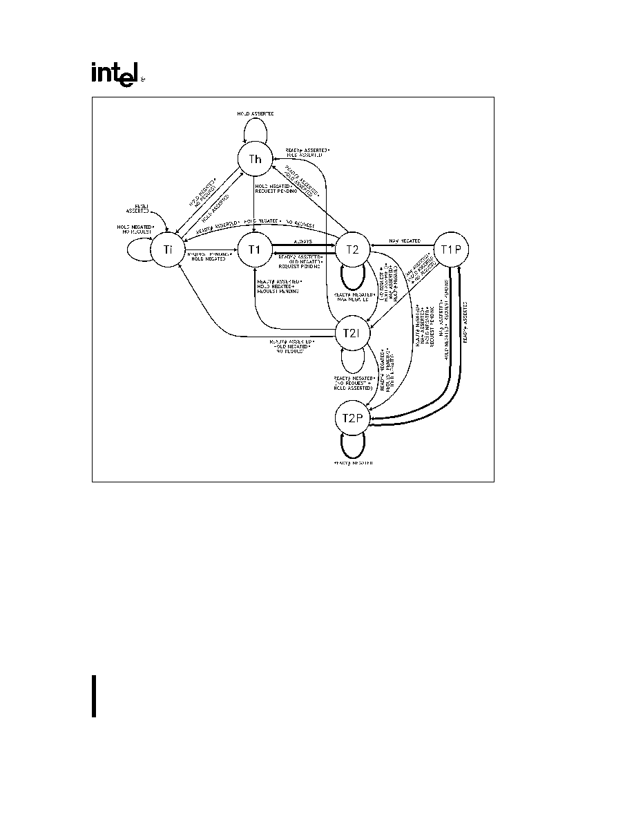
Intel386
TM
DX MICROPROCESSOR
Bus States
T1
first clock of a non-pipelined bus cycle (Intel386 DX drives new ad-
dress and asserts ADS )
T2
subsequent clocks of a bus cycle when NA
has not been sampled
asserted in the current bus cycle
T2I
subsequent clocks of a bus cycle when NA
has been sampled as-
serted in the current bus cycle but there is not yet an internal bus request
pending (Intel386 DX will not drive new address or assert ADS )
T2P
subsequent clocks of a bus cycle when NA
has been sampled
asserted in the current bus cycle and there is an internal bus request pend-
ing (Intel386 DX drives new address and asserts ADS )
T1P
first clock of a pipelined bus cycle
Ti
idle state
Th
hold acknowledge state (Intel386 DX asserts HLDA)
Asserting NA
for pipelined address gives access to three more bus
states T2I T2P and T1P
Using pipelined address the fastest bus cycle consists of T1P and T2P
231630 � 24
Figure 5-20 Intel386
TM
DX Complete Bus States (including pipelined address)
Realistically address pipelining is almost always
maintained as long as NA
is sampled asserted
This is so because in the absence of any other re-
quest a code prefetch request is always internally
pending until the instruction decoder and code pre-
fetch queue are completely full Therefore address
pipelining is maintained for long bursts of bus cycles
if the bus is available (i e HOLD negated) and NA
is sampled asserted in each of the bus cycles
5 4 3 6 PIPELINED ADDRESS WITH DYNAMIC
DATA BUS SIZING
The BS16
feature allows easy interface to 16-bit
data buses When asserted the Intel386 DX bus
interface hardware performs appropriate action to
make the transfer using a 16-bit data bus connected
on D0 � D15
There is a degree of interaction however between
the use of Address Pipelining and the use of Bus
Size 16 The interaction results from the multiple bus
cycles required when transferring 32-bit operands
over a 16-bit bus If the operand requires both 16-bit
halves of the 32-bit bus the appropriate Intel386 DX
action is a second bus cycle to complete the oper-
and's transfer It is this necessity that conflicts with
NA
usage
When NA
is sampled asserted the Intel386 DX
commits
itself
to
perform
the
next
inter-
85

Intel386
TM
DX MICROPROCESSOR
nally pending bus request and is allowed to drive
the next internally pending address onto the bus As-
serting NA
therefore makes it impossible for the
next bus cycle to again access the current address
on A2 � A31 such as may be required when BS16
is asserted by the external hardware
To avoid conflict the Intel386 DX is designed with
following two provisions
1) To avoid conflict BS16
must be negated in the
current bus cycle if NA
has already been
sampled asserted in the current cycle If NA
is
sampled asserted the current data bus size is as-
sumed to be 32 bits
2) To also avoid conflict if NA
and BS16
are
both asserted during the same sampling window
BS16
asserted has priority and the Intel386 DX
acts as if NA
was negated at that time Internal
Intel386 DX circuitry shown conceptually in Fig-
ure 5-18 assures that BS16
is sampled assert-
ed and NA
is sampled negated if both inputs
are externally asserted at the same sampling win-
dow
Key Dn e physical data pin n
231630 � 25
dn e logical data bit n
Cycle 1 is pipelined Cycle 1a cannot be pipelined but its address can be inferred from that of Cycle 1 to externally simulate address pipelining
during Cycle 1a
Figure 5-21 Using NA
and BS16
86

Intel386
TM
DX MICROPROCESSOR
Certain types of 16-bit or 8-bit operands require no
adjustment for correct transfer on a 16-bit bus
Those are read or write operands using only the low-
er half of the data bus and write operands using
only the upper half of the bus since the Intel386 DX
simultaneously duplicates the write data on the low-
er half of the data bus For these patterns of Byte
Enables and the R W
signals BS16
need not be
asserted at the Intel386 DX allowing NA
to be as-
serted during the bus cycle if desired
5 4 4 Interrupt Acknowledge (INTA)
Cycles
In response to an interrupt request on the INTR in-
put when interrupts are enabled the Intel386 DX
performs two interrupt acknowledge cycles These
bus cycles are similar to read cycles in that bus defi-
nition signals define the type of bus activity taking
place and each cycle continues until acknowledged
by READY
sampled asserted
The state of A2 distinguishes the first and second
interrupt acknowledge cycles
The byte address
driven during the first interrupt acknowledge cycle is
4 (A31 � A3 low A2 high BE3
� BE1
high and
BE0
low) The address driven during the second
interrupt acknowledge cycle is 0 (A31 � A2 low
BE3
� BE1
high BE0
low)
231630 � 26
Interrupt Vector (0 � 255) is read on D0 � D7 at end of second Interrupt Acknowledge bus cycle
Because each Interrupt Acknowledge bus cycle is followed by idle bus states asserting NA
has no practical effect Choose the approach
which is simplest for your system hardware design
Figure 5-22 Interrupt Acknowledge Cycles
87

Intel386
TM
DX MICROPROCESSOR
231630 � 27
Figure 5-23 Halt Indication Cycle
The LOCK
output is asserted from the beginning
of the first interrupt acknowledge cycle until the end
of the second interrupt acknowledge cycle Four idle
bus states Ti are inserted by the Intel386 DX be-
tween the two interrupt acknowledge cycles allow-
ing for compatibility with spec TRHRL of the 8259A
Interrupt Controller
During both interrupt acknowledge cycles D0 � D31
float No data is read at the end of the first interrupt
acknowledge cycle At the end of the second inter-
rupt acknowledge cycle the Intel386 DX will read an
external interrupt vector from D0 � D7 of the data
bus The vector indicates the specific interrupt num-
ber (from 0 � 255) requiring service
5 4 5 Halt Indication Cycle
The Intel386 DX halts as a result of executing a
HALT instruction Signaling its entrance into the halt
state a halt indication cycle is performed The halt
indication cycle is identified by the state of the bus
definition signals shown in 5 2 5 Bus Cycle Defini-
tion
and a byte address of 2 BE0
and BE2
are
the only signals distinguishing halt indication from
shutdown indication which drives an address of 0
During the halt cycle undefined data is driven on
D0 � D31 The halt indication cycle must be acknowl-
edged by READY
asserted
A halted Intel386 DX resumes execution when INTR
(if interrupts are enabled) or NMI or RESET is as-
serted
88

Intel386
TM
DX MICROPROCESSOR
5 4 6 Shutdown Indication Cycle
The Intel386 DX shuts down as a result of a protec-
tion fault while attempting to process a double fault
Signaling its entrance into the shutdown state a
shutdown indication cycle is performed The shut-
down indication cycle is identified by the state of the
bus definition signals shown in 5 2 5 Bus Cycle Def-
inition
and a byte address of 0 BE0
and BE2
are the only signals distinguishing shutdown indica-
tion from halt indication which drives an address of
2 During the shutdown cycle undefined data is driv-
en on D0 � D31 The shutdown indication cycle must
be acknowledged by READY
asserted
A shutdown Intel386 DX resumes execution when
NMI or RESET is asserted
231630 � 28
Figure 5-24 Shutdown Indication Cycle
89

Intel386
TM
DX MICROPROCESSOR
5 5 OTHER FUNCTIONAL
DESCRIPTIONS
5 5 1 Entering and Exiting Hold
Acknowledge
The bus hold acknowledge state Th is entered in
response to the HOLD input being asserted In the
bus hold acknowledge state the Intel386 DX floats
all output or bidirectional signals except for HLDA
HLDA is asserted as long as the Intel386 DX re-
mains in the bus hold acknowledge state In the bus
hold acknowledge state all inputs except HOLD
RESET BUSY
ERROR
and PEREQ are ig-
nored (also up to one rising edge on NMI is remem-
bered for processing when HOLD is no longer as-
serted)
231630 � 29
NOTE
For maximum design flexibility the Intel386 DX has no
internal pullup resistors on its outputs Your design may
require an external pullup on ADS
and other Intel386
DX outputs to keep them negated during float periods
Figure 5-25 Requesting Hold from Idle Bus
Th may be entered from a bus idle state as in Figure
5-25 or after the acknowledgement of the current
physical bus cycle if the LOCK
signal is not assert-
ed as in Figures 5-26 and 5-27 If HOLD is asserted
during a locked bus cycle the Intel386 DX may exe-
cute one unlocked bus cycle before acknowledging
HOLD If asserting BS16
requires a second 16-bit
bus cycle to complete a physical operand transfer it
is performed before HOLD is acknowledged al-
though the bus state diagrams in Figures 5-13 and
5-20 do not indicate that detail
Th is exited in response to the HOLD input being
negated The following state will be Ti as in Figure
5-25 if no bus request is pending The following bus
state will be T1 if a bus request is internally pending
as in Figures 5-26 and 5-27
Th is also exited in response to RESET being assert-
ed
If a rising edge occurs on the edge-triggered NMI
input while in Th the event is remembered as a non-
maskable interrupt 2 and is serviced when Th is exit-
ed unless of course the Intel386 DX is reset before
Th is exited
5 5 2 Reset During Hold Acknowledge
RESET being asserted takes priority over HOLD be-
ing asserted Therefore Th is exited in reponse to
the RESET input being asserted If RESET is assert-
ed while HOLD remains asserted the Intel386 DX
drives its pins to defined states during reset as in
Table 5-3 Pin State During Reset
and performs
internal reset activity as usual
If HOLD remains asserted when RESET is negated
the Intel386 DX enters the hold acknowledge state
before performing its first bus cycle provided HOLD
is still asserted when the Intel386 DX would other-
wise perform its first bus cycle If HOLD remains as-
serted when RESET is negated the BUSY
input is
still sampled as usual to determine whether a self
test is being requested and ERROR
is still sam-
pled as usual to determine whether a Intel387 DX
coprocessor vs an 80287 (or none) is present
5 5 3 Bus Activity During and
Following Reset
RESET is the highest priority input signal capable of
interrupting any processor activity when it is assert-
ed A bus cycle in progress can be aborted at any
stage or idle states or bus hold acknowledge states
discontinued so that the reset state is established
RESET should remain asserted for at least 15 CLK2
periods to ensure it is recognized throughout the In-
tel386 DX and at least 80 CLK2 periods if Intel386
DX self-test is going to be requested at the falling
edge RESET asserted pulses less than 15 CLK2
periods may not be recognized RESET pulses less
than 80 CLK2 periods followed by a self-test may
90
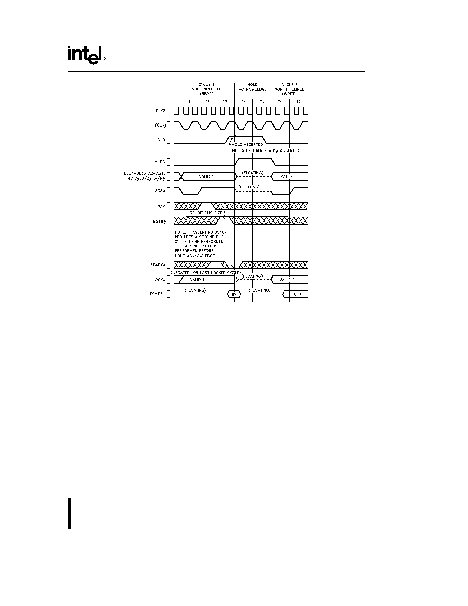
Intel386
TM
DX MICROPROCESSOR
231630 � 30
NOTE
HOLD is a synchronous input and can be asserted at any CLK2 edge provided setup and hold (t
23
and t
24
) require-
ments are met This waveform is useful for determining Hold Acknowledge latency
Figure 5-26 Requesting Hold from Active Bus (NA
negated)
cause the self-test to report a failure when no true
failure exists The additional RESET pulse width is
required to clear additional state prior to a valid self-
test
Provided the RESET falling edge meets setup and
hold times t
25
and t
26
the internal processor clock
phase is defined at that time as illustrated by Figure
5-28 and Figure 7-7
A Intel386 DX self-test may be requested at the time
RESET is negated by having the BUSY
input at a
LOW level as shown in Figure 5-28 The self-test
requires (2
20
) a approximately 60 CLK2 periods to
complete The self-test duration is not affected by
the test results Even if the self-test indicates a prob-
lem the Intel386 DX attempts to proceed with the
reset sequence afterwards
After the RESET falling edge (and after the self-test
if it was requested) the Intel386 DX performs an in-
ternal initialization sequence for approximately 350
to 450 CLK2 periods
The Intel386 DX samples its ERROR
input some
time after the falling edge of RESET and before exe-
cuting the first ESC instruction During this sampling
period BUSY
must be HIGH If ERROR
was
sampled active the Intel386 DX employs the 32-bit
protocol of the Intel387 DX Even though this proto-
col was selected it is still necessary to use a soft-
ware recognition test to determine the presence or
identity of the coprocessor and to assure compatibil-
ity with future processors (See Chapter 11 of the
Intel386 DX Programmer's Reference Manual Order
230985-002)
91

Intel386
TM
DX MICROPROCESSOR
231630 � 31
NOTE
HOLD is a synchronous input and can be asserted at any CLK2 edge provided setup and hold (t
23
and t
24
) require-
ments are met This waveform is useful for determining Hold Acknowledge latency
Figure 5-27 Requesting Hold from Active Bus (NA
asserted)
5 6 SELF-TEST SIGNATURE
Upon completion of self-test (if self-test was re-
quested by holding BUSY
LOW at least eight
CLK2 periods before and after the falling edge of
RESET) the EAX register will contain a signature of
00000000h indicating the Intel386 DX passed its
self-test of microcode and major PLA contents with
no problems detected The passing signature in
EAX 00000000h applies to all Intel386 DX revision
levels Any non-zero signature indicates the Intel386
DX unit is faulty
5 7 COMPONENT AND REVISION
IDENTIFIERS
To assist Intel386 DX users the Intel386 DX after
reset holds a component identifier and a revision
identifier in its DX register The upper 8 bits of DX
hold 03h as identification of the Intel386 DX compo-
nent The lower 8 bits of DX hold an 8-bit unsigned
binary number related to the component revision
level The revision identifier begins chronologically
with a value zero and is subject to change (typically
it will be incremented) with component steppings in-
tended to have certain improvements or distinctions
from previous steppings
These features are intended to assist Intel386 DX
users to a practical extent However the revision
identifier value is not guaranteed to change with ev-
ery stepping revision or to follow a completely uni-
form numerical sequence depending on the type or
intention of revision or manufacturing materials re-
quired to be changed Intel has sole discretion over
these characteristics of the component
92

Intel386
TM
DX MICROPROCESSOR
231630 � 32
NOTES
1 BUSY
should be held stable for 8 CLK2 periods before and after the CLK2 period in which RESET falling edge
occurs
2 If self-test is requested the Intel386 DX outputs remain in their reset state as shown here and in Table 5-3
Figure 5-28 Bus Activity from Reset Until First Code Fetch
Table 5-10 Component and Revision Identifier History
Intel386
TM
DX
Component
Revision
Intel386 DX
Component
Revision
Stepping
Identifier
Identifier
Stepping
Identifier
Identifier
Name
Name
B0
03
03
D0
03
05
B1
03
03
D1
03
08
93

Intel386
TM
DX MICROPROCESSOR
5 8 COPROCESSOR INTERFACING
The Intel386 DX provides an automatic interface for
the Intel Intel387 DX numeric floating-point coproc-
essor The Intel387 DX coprocessor uses an I O-
mapped interface driven automatically by the In-
tel386 DX and assisted by three dedicated signals
BUSY
ERROR
and PEREQ
As the Intel386 DX begins supporting a coprocessor
instruction it tests the BUSY
and ERROR
sig-
nals to determine if the coprocessor can accept its
next instruction Thus the BUSY
and ERROR
inputs eliminate the need for any ``preamble'' bus
cycles for communication between processor and
coprocessor The Intel387 DX can be given its com-
mand opcode immediately The dedicated signals
provide instruction synchronization and eliminate
the need of using the Intel386 DX WAIT opcode
(9Bh) for Intel387 DX coprocessor instruction syn-
chronization (the WAIT opcode was required when
8086 or 8088 was used with the 8087 coprocessor)
Custom coprocessors can be included in Intel386
DX-based systems via memory-mapped or I O-
mapped interfaces Such coprocessor interfaces al-
low a completely custom protocol and are not limit-
ed to a set of coprocessor protocol ``primitives'' In-
stead memory-mapped or I O-mapped interfaces
may use all applicable Intel386 DX instructions for
high-speed
coprocessor
communication
The
BUSY
and ERROR
inputs of the Intel386 DX
may also be used for the custom coprocessor inter-
face if such hardware assist is desired These sig-
nals can be tested by the Intel386 DX WAIT opcode
(9Bh)
The WAIT instruction will wait until the
BUSY
input is negated (interruptable by an NMI or
enabled INTR input) but generates an exception 16
fault if the ERROR
pin is in the asserted state
when the BUSY
goes (or is) negated If the custom
coprocessor interface is memory-mapped protec-
tion of the addresses used for the interface can be
provided with the Intel386 DX on-chip paging or
segmentation mechanisms If the custom interface
is I O-mapped protection of the interface can be
provided with the Intel386 DX IOPL (I O Privilege
Level) mechanism
The Intel387 DX numeric coprocessor interface is
I O mapped as shown in Table 5-11 Note that the
Intel387 DX coprocessor interface addresses are
beyond the 0h-FFFFh range for programmed I O
When the Intel386 DX supports the Intel387 DX co-
processor the Intel386 DX automatically generates
bus cycles to the coprocessor interface addresses
Table 5-11 Numeric Coprocessor
Port Addresses
Address in
Intel387
TM
DX
Intel386
TM
DX
Coprocessor
I O Space
Register
800000F8h
Opcode Register
(32-bit port)
800000FCh
Operand Register
(32-bit port)
To correctly map the Intel387 DX coprocessor regis-
ters to the appropriate I O addresses connect the
Intel387 DX coprocessor CMD0
pin directly to the
A2 output of the Intel386 DX
5 8 1 Software Testing for
Coprocessor Presence
When software is used to test for coprocessor (In-
tel387 DX) presence it should use only the following
coprocessor opcodes FINIT FNINIT FSTCW mem
FSTSW mem FSTSW AX To use other coproces-
sor opcodes when a coprocessor is known to be not
present first set EM e 1 in Intel386 DX CR0
94

Intel386
TM
DX MICROPROCESSOR
6 INSTRUCTION SET
This section describes the Intel386 DX instruction
set A table lists all instructions along with instruction
encoding diagrams and clock counts Further details
of the instruction encoding are then provided in the
following sections which completely describe the
encoding structure and the definition of all fields oc-
curring within Intel386 DX instructions
6 1 Intel386
TM
DX INSTRUCTION
ENCODING AND CLOCK COUNT
SUMMARY
To calculate elapsed time for an instruction multiply
the instruction clock count as listed in Table 6-1
below by the processor clock period (e g 50 ns for
a 20 MHz Intel386 DX 40 ns for a 25 MHz Intel386
DX and 30 ns for a 33 MHz Intel386 DX)
For more detailed information on the encodings of
instructions refer to section 6 2 Instruction Encod-
ings Section 6 2 explains the general structure of
instruction encodings and defines exactly the en-
codings of all fields contained within the instruction
Instruction Clock Count Assumptions
1 The instruction has been prefetched decoded
and is ready for execution
2 Bus cycles do not require wait states
3 There are no local bus HOLD requests delaying
processor access to the bus
4 No exceptions are detected during instruction ex-
ecution
5 If an effective address is calculated it does not
use two general register components One regis-
ter scaling and displacement can be used within
the clock counts shown However if the effective
address calculation uses two general register
components add 1 clock to the clock count
shown
Instruction Clock Count Notation
1 If two clock counts are given the smaller refers to
a register operand and the larger refers to a mem-
ory operand
2 n e number of times repeated
3 m e number of components in the next instruc-
tion executed where the entire displacement (if
any) counts as one component the entire imme-
diate data (if any) counts as one component and
each of the other bytes of the instruction and pre-
fix(es) each count as one component
Wait States
Add 1 clock per wait state to instruction execution
for each data access
95

Intel386
TM
DX MICROPROCESSOR
Table 6-1 Intel386
TM
DX Instruction Set Clock Count Summary
CLOCK COUNT
NOTES
Real
Real
INSTRUCTION
FORMAT
Address
Protected
Address
Protected
Mode or
Virtual
Mode or
Virtual
Virtual
Address
Virtual
Address
8086
Mode
8086
Mode
Mode
Mode
GENERAL DATA TRANSFER
MOV
e
Move
Register to Register Memory
1 0 0 0 1 0 0 w
mod reg
r m
2 2
2 2
b
h
Register Memory to Register
1 0 0 0 1 0 1 w
mod reg
r m
2 4
2 4
b
h
Immediate to Register Memory
1 1 0 0 0 1 1 w
mod 0 0 0
r m
immediate data
2 2
2 2
b
h
Immediate to Register (short form)
1 0 1 1 w
reg
immediate data
2
2
Memory to Accumulator (short form)
1 0 1 0 0 0 0 w
full displacement
4
4
b
h
Accumulator to Memory (short form)
1 0 1 0 0 0 1 w
full displacement
2
2
b
h
Register Memory to Segment Register
1 0 0 0 1 1 1 0
mod sreg3 r m
2 5
18 19
b
h i j
Segment Register to Register Memory
1 0 0 0 1 1 0 0
mod sreg3 r m
2 2
2 2
b
h
MOVSX
e
Move With Sign Extension
Register From Register Memory
0 0 0 0 1 1 1 1
1 0 1 1 1 1 1 w
mod reg
r m
3 6
3 6
b
h
MOVZX
e
Move With Zero Extension
Register From Register Memory
0 0 0 0 1 1 1 1
1 0 1 1 0 1 1 w
mod reg
r m
3 6
3 6
b
h
PUSH
e
Push
Register Memory
1 1 1 1 1 1 1 1
mod 1 1 0
r m
5
5
b
h
Register (short form)
0 1 0 1 0
reg
2
2
b
h
Segment Register (ES CS SS or DS)
0 0 0 sreg2 1 1 0
2
2
b
h
Segment Register (FS or GS)
0 0 0 0 1 1 1 1
1 0 sreg3 0 0 0
2
2
b
h
Immediate
0 1 1 0 1 0 s 0
immediate data
2
2
b
h
PUSHA
e
Push All
0 1 1 0 0 0 0 0
18
18
b
h
POP
e
Pop
Register Memory
1 0 0 0 1 1 1 1
mod 0 0 0
r m
5
5
b
h
Register (short form)
0 1 0 1 1
reg
4
4
b
h
Segment Register (ES SS or DS)
0 0 0 sreg 2 1 1 1
7
21
b
h i j
Segment Register (FS or GS)
0 0 0 0 1 1 1 1
1 0 sreg 3 0 0 1
7
21
b
h i j
POPA
e
Pop All
0 1 1 0 0 0 0 1
24
24
b
h
XCHG
e
Exchange
Register Memory With Register
1 0 0 0 0 1 1 w
mod reg
r m
3 5
3 5
b f
f h
Register With Accumulator (short form)
1 0 0 1 0
reg
8086 Mode
Clk Count
Virtual
3
3
IN
e
Input from
Fixed Port
1 1 1 0 0 1 0 w
port number
26
12
6
26
m
Variable Port
1 1 1 0 1 1 0 w
27
13
7
27
m
OUT
e
Output to
Fixed Port
1 1 1 0 0 1 1 w
port number
24
10
4
24
m
Variable Port
1 1 1 0 1 1 1 w
25
11
5
25
m
LEA
e
Load EA to Register
1 0 0 0 1 1 0 1
mod reg
r m
2
2
If CPL
s
IOPL
If CPL
l
IOPL
96

Intel386
TM
DX MICROPROCESSOR
Table 6-1 Intel386
TM
DX Instruction Set Clock Count Summary
(Continued)
CLOCK COUNT
NOTES
Real
Real
INSTRUCTION
FORMAT
Address
Protected
Address
Protected
Mode or
Virtual
Mode or
Virtual
Virtual
Address
Virtual
Address
8086
Mode
8086
Mode
Mode
Mode
SEGMENT CONTROL
LDS
e
Load Pointer to DS
1 1 0 0 0 1 0 1
mod reg
r m
7
22
b
h i j
LES
e
Load Pointer to ES
1 1 0 0 0 1 0 0
mod reg
r m
7
22
b
h i j
LFS
e
Load Pointer to FS
0 0 0 0 1 1 1 1
1 0 1 1 0 1 0 0
mod reg
r m
7
25
b
h i j
LGS
e
Load Pointer to GS
0 0 0 0 1 1 1 1
1 0 1 1 0 1 0 1
mod reg
r m
7
25
b
h i j
LSS
e
Load Pointer to SS
0 0 0 0 1 1 1 1
1 0 1 1 0 0 1 0
mod reg
r m
7
22
b
h i j
FLAG CONTROL
CLC
e
Clear Carry Flag
1 1 1 1 1 0 0 0
2
2
CLD
e
Clear Direction Flag
1 1 1 1 1 1 0 0
2
2
CLI
e
Clear Interrupt Enable Flag
1 1 1 1 1 0 1 0
8
8
m
CLTS
e
Clear Task Switched Flag
0 0 0 0 1 1 1 1
0 0 0 0 0 1 1 0
6
6
c
l
CMC
e
Complement Carry Flag
1 1 1 1 0 1 0 1
2
2
LAHF
e
Load AH into Flag
1 0 0 1 1 1 1 1
2
2
POPF
e
Pop Flags
1 0 0 1 1 1 0 1
5
5
b
h n
PUSHF
e
Push Flags
1 0 0 1 1 1 0 0
4
4
b
h
SAHF
e
Store AH into Flags
1 0 0 1 1 1 1 0
3
3
STC
e
Set Carry Flag
1 1 1 1 1 0 0 1
2
2
STD
e
Set Direction Flag
1 1 1 1 1 1 0 1
2
2
STI
e
Set Interrupt Enable Flag
1 1 1 1 1 0 1 1
8
8
m
ARITHMETIC
ADD
e
Add
Register to Register
0 0 0 0 0 0 d w
mod reg
r m
2
2
Register to Memory
0 0 0 0 0 0 0 w
mod reg
r m
7
7
b
h
Memory to Register
0 0 0 0 0 0 1 w
mod reg
r m
6
6
b
h
Immediate to Register Memory
1 0 0 0 0 0 s w
mod 0 0 0
r m
immediate data
2 7
2 7
b
h
Immediate to Accumulator (short form)
0 0 0 0 0 1 0 w
immediate data
2
2
ADC
e
Add With Carry
Register to Register
0 0 0 1 0 0 d w
mod reg
r m
2
2
Register to Memory
0 0 0 1 0 0 0 w
mod reg
r m
7
7
b
h
Memory to Register
0 0 0 1 0 0 1 w
mod reg
r m
6
6
b
h
Immediate to Register Memory
1 0 0 0 0 0 s w
mod 0 1 0
r m
immediate data
2 7
2 7
b
h
Immediate to Accumulator (short form)
0 0 0 1 0 1 0 w
immediate data
2
2
INC
e
Increment
Register Memory
1 1 1 1 1 1 1 w
mod 0 0 0
r m
2 6
2 6
b
h
Register (short form)
0 1 0 0 0
reg
2
2
SUB
e
Subtract
Register from Register
0 0 1 0 1 0 d w
mod reg
r m
2
2
97

Intel386
TM
DX MICROPROCESSOR
Table 6-1 Intel386
TM
DX Instruction Set Clock Count Summary
(Continued)
CLOCK COUNT
NOTES
Real
Real
INSTRUCTION
FORMAT
Address
Protected
Address
Protected
Mode or
Virtual
Mode or
Virtual
Virtual
Address
Virtual
Address
8086
Mode
8086
Mode
Mode
Mode
ARITHMETIC
(Continued)
Register from Memory
0 0 1 0 1 0 0 w mod reg
r m
7
7
b
h
Memory from Register
0 0 1 0 1 0 1 w mod reg
r m
6
6
b
h
Immediate from Register Memory
1 0 0 0 0 0 s w mod 1 0 1
r m immediate data
2 7
2 7
b
h
Immediate from Accumulator (short form)
0 0 1 0 1 1 0 w
immediate data
2
2
SBB
e
Subtract with Borrow
Register from Register
0 0 0 1 1 0 d w mod reg
r m
2
2
Register from Memory
0 0 0 1 1 0 0 w mod reg
r m
7
7
b
h
Memory from Register
0 0 0 1 1 0 1 w mod reg
r m
6
6
b
h
Immediate from Register Memory
1 0 0 0 0 0 s w mod 0 1 1
r m immediate data
2 7
2 7
b
h
Immediate from Accumulator (short form)
0 0 0 1 1 1 0 w
immediate data
2
2
DEC
e
Decrement
Register Memory
1 1 1 1 1 1 1 w reg 0 0 1
r m
2 6
2 6
b
h
Register (short form)
0 1 0 0 1
reg
2
2
CMP
e
Compare
Register with Register
0 0 1 1 1 0 d w mod reg
r m
2
2
Memory with Register
0 0 1 1 1 0 0 w mod reg
r m
5
5
b
h
Register with Memory
0 0 1 1 1 0 1 w mod reg
r m
6
6
b
h
Immediate with Register Memory
1 0 0 0 0 0 s w mod 1 1 1
r m immediate data
2 5
2 5
b
h
Immediate with Accumulator (short form)
0 0 1 1 1 1 0 w
immediate data
2
2
NEG
e
Change Sign
1 1 1 1 0 1 1 w mod 0 1 1
r m
2 6
2 6
b
h
AAA
e
ASCII Adjust for Add
0 0 1 1 0 1 1 1
4
4
AAS
e
ASCII Adjust for Subtract
0 0 1 1 1 1 1 1
4
4
DAA
e
Decimal Adjust for Add
0 0 1 0 0 1 1 1
4
4
DAS
e
Decimal Adjust for Subtract
0 0 1 0 1 1 1 1
4
4
MUL
e
Multiply (unsigned)
Accumulator with Register Memory
1 1 1 1 0 1 1 w mod 1 0 0
r m
Multiplier-Byte
12�17 15-20 12�17 15�20
b d
d h
-Word
12�25 15-28 12�25 15�28
b d
d h
-Doubleword
12�41 15-44 12�41 15�44
b d
d h
IMUL
e
Integer Multiply (signed)
Accumulator with Register Memory
1 1 1 1 0 1 1 w mod 1 0 1
r m
Multiplier-Byte
12�17 15-20 12�17 15�20
b d
d h
-Word
12�25 15-28 12�25 15�28
b d
d h
-Doubleword
12�41 15-44 12�41 15�44
b d
d h
Register with Register Memory
0 0 0 0 1 1 1 1
1 0 1 0 1 1 1 1
mod reg
r m
Multiplier-Byte
12�17 15-20 12�17 15�20
b d
d h
-Word
12�25 15-28 12�25 15�28
b d
d h
-Doubleword
12�41 15-44 12�41 15�44
b d
d h
Register Memory with Immediate to Register
0 1 1 0 1 0 s 1
mod reg
r m immediate data
-Word
13�26 14-27 13�26 14�27
b d
d h
-Doubleword
13�42 14-43 13�42 14�43
b d
d h
98

Intel386
TM
DX MICROPROCESSOR
Table 6-1 Intel386
TM
DX Instruction Set Clock Count Summary
(Continued)
CLOCK COUNT
NOTES
Real
Real
INSTRUCTION
FORMAT
Address Protected Address Protected
Mode or
Virtual
Mode or
Virtual
Virtual
Address
Virtual
Address
8086
Mode
8086
Mode
Mode
Mode
ARITHMETIC
(Continued)
DIV
e
Divide (Unsigned)
Accumulator by Register Memory
1 1 1 1 0 1 1 w mod 1 1 0
r m
Divisor
Byte
14 17
14 17
b e
e h
Word
22 25
22 25
b e
e h
Doubleword
38 41
38 41
b e
e h
IDIV
e
Integer Divide (Signed)
Accumulator By Register Memory
1 1 1 1 0 1 1 w mod 1 1 1
r m
Divisor
Byte
19 22
19 22
b e
e h
Word
27 30
27 30
b e
e h
Doubleword
43 46
43 46
b e
e h
AAD
e
ASCII Adjust for Divide
1 1 0 1 0 1 0 1
0 0 0 0 1 0 1 0
19
19
AAM
e
ASCII Adjust for Multiply
1 1 0 1 0 1 0 0
0 0 0 0 1 0 1 0
17
17
CBW
e
Convert Byte to Word
1 0 0 1 1 0 0 0
3
3
CWD
e
Convert Word to Double Word
1 0 0 1 1 0 0 1
2
2
LOGIC
Shift Rotate Instructions
Not Through Carry (ROL ROR SAL SAR SHL and SHR)
Register Memory by 1
1 1 0 1 0 0 0 w mod TTT
r m
3 7
3 7
b
h
Register Memory by CL
1 1 0 1 0 0 1 w mod TTT
r m
3 7
3 7
b
h
Register Memory by Immediate Count
1 1 0 0 0 0 0 w mod TTT
r m immed 8-bit data
3 7
3 7
b
h
Through Carry (RCL and RCR)
Register Memory by 1
1 1 0 1 0 0 0 w mod TTT
r m
9 10
9 10
b
h
Register Memory by CL
1 1 0 1 0 0 1 w mod TTT
r m
9 10
9 10
b
h
Register Memory by Immediate Count
1 1 0 0 0 0 0 w mod TTT
r m immed 8-bit data
9 10
9 10
b
h
T T T Instruction
0 0 0
ROL
0 0 1
ROR
0 1 0
RCL
0 1 1
RCR
1 0 0
SHL SAL
1 0 1
SHR
1 1 1
SAR
SHLD
e
Shift Left Double
Register Memory by Immediate
0 0 0 0 1 1 1 1
1 0 1 0 0 1 0 0 mod reg
r m immed 8-bit data
3 7
3 7
Register Memory by CL
0 0 0 0 1 1 1 1
1 0 1 0 0 1 0 1 mod reg
r m
3 7
3 7
SHRD
e
Shift Right Double
Register Memory by Immediate
0 0 0 0 1 1 1 1
1 0 1 0 1 1 0 0 mod reg
r m immed 8-bit data
3 7
3 7
Register Memory by CL
0 0 0 0 1 1 1 1
1 0 1 0 1 1 0 1 mod reg
r m
3 7
3 7
AND
e
And
Register to Register
0 0 1 0 0 0 d w mod reg
r m
2
2
99

Intel386
TM
DX MICROPROCESSOR
Table 6-1 Intel386
TM
DX Instruction Set Clock Count Summary
(Continued)
CLOCK COUNT
NOTES
Real
Real
INSTRUCTION
FORMAT
Address
Protected
Address
Protected
Mode or
Virtual
Mode or
Virtual
Virtual
Address
Virtual
Address
8086
Mode
8086
Mode
Mode
Mode
LOGIC
(Continued)
Register to Memory
0 0 1 0 0 0 0 w
mod reg
r m
7
7
b
h
Memory to Register
0 0 1 0 0 0 1 w
mod reg
r m
6
6
b
h
Immediate to Register Memory
1 0 0 0 0 0 s w
mod 1 0 0
r m immediate data
2 7
2 7
b
h
Immediate to Accumulator (Short Form)
0 0 1 0 0 1 0 w
immediate data
2
2
TEST
e
And Function to Flags No Result
Register Memory and Register
1 0 0 0 0 1 0 w
mod reg
r m
2 5
2 5
b
h
Immediate Data and Register Memory
1 1 1 1 0 1 1 w
mod 0 0 0
r m immediate data
2 5
2 5
b
h
Immediate Data and Accumulator
(Short Form)
1 0 1 0 1 0 0 w
immediate data
2
2
OR
e
Or
Register to Register
0 0 0 0 1 0 d w
mod reg
r m
2
2
Register to Memory
0 0 0 0 1 0 0 w
mod reg
r m
7
7
b
h
Memory to Register
0 0 0 0 1 0 1 w
mod reg
r m
6
6
b
h
Immediate to Register Memory
1 0 0 0 0 0 s w
mod 0 0 1
r m immediate data
2 7
2 7
b
h
Immediate to Accumulator (Short Form)
0 0 0 0 1 1 0 w
immediate data
2
2
XOR
e
Exclusive Or
Register to Register
0 0 1 1 0 0 d w
mod reg
r m
2
2
Register to Memory
0 0 1 1 0 0 0 w
mod reg
r m
7
7
b
h
Memory to Register
0 0 1 1 0 0 1 w
mod reg
r m
6
6
b
h
Immediate to Register Memory
1 0 0 0 0 0 s w
mod 1 1 0
r m immediate data
2 7
2 7
b
h
Immediate to Accumulator (Short Form)
0 0 1 1 0 1 0 w
immediate data
2
2
NOT
e
Invert Register Memory
1 1 1 1 0 1 1 w
mod 0 1 0
r m
2 6
2 6
b
h
STRING MANIPULATION
CMPS
e
Compare Byte Word
1 0 1 0 0 1 1 w
Virtual
Count
Mode
8086
Clk
10
10
b
h
INS
e
Input Byte Word from DX Port
0 1 1 0 1 1 0 w
29
15
9
29
b
h m
LODS
e
Load Byte Word to AL AX EAX
1 0 1 0 1 1 0 w
5
5
b
h
MOVS
e
Move Byte Word
1 0 1 0 0 1 0 w
8
8
b
h
OUTS
e
Output Byte Word to DX Port
0 1 1 0 1 1 1 w
28
14
8
28
b
h m
SCAS
e
Scan Byte Word
1 0 1 0 1 1 1 w
8
8
b
h
STOS
e
Store Byte Word from
AL AX EX
1 0 1 0 1 0 1 w
5
5
b
h
XLAT
e
Translate String
1 1 0 1 0 1 1 1
5
5
h
REPEATED STRING MANIPULATION
Repeated by Count in CX or ECX
REPE CMPS
e
Compare String
(Find Non-Match)
1 1 1 1 0 0 1 1
1 0 1 0 0 1 1 w
5
a
9n
5
a
9n
b
h
If CPL
s
IOPL
If CPL
l
IOPL
100

Intel386
TM
DX MICROPROCESSOR
Table 6-1 Intel386
TM
DX Instruction Set Clock Count Summary
(Continued)
CLOCK COUNT
NOTES
Real
Real
INSTRUCTION
FORMAT
Address
Protected
Address Protected
Mode or
Virtual
Mode or
Virtual
Virtual
Address
Virtual
Address
8086
Mode
8086
Mode
Mode
Mode
REPEATED STRING MANIPULATION
(Continued)
REPNE CMPS
e
Compare String
(Find Match)
1 1 1 1 0 0 1 0
1 0 1 0 0 1 1 w
8086 Mode
Clk Count
Virtual
5
a
9n
5
a
9n
b
h
REP INS
e
Input String
1 1 1 1 0 0 1 0
0 1 1 0 1 1 0 w
28
a
6n
14
a
6n 8
a
6n
28
a
6n
b
h m
REP LODS
e
Load String
1 1 1 1 0 0 1 0
1 0 1 0 1 1 0 w
5
a
6n
5
a
6n
b
h
REP MOVS
e
Move String
1 1 1 1 0 0 1 0
1 0 1 0 0 1 0 w
8
a
4n
8
a
4n
b
h
REP OUTS
e
Output String
1 1 1 1 0 0 1 0
0 1 1 0 1 1 1 w
26
a
5n
12
a
5n 6
a
5n
26
a
5n
b
h m
REPE SCAS
e
Scan String
(Find Non-AL AX EAX)
1 1 1 1 0 0 1 1
1 0 1 0 1 1 1 w
5
a
8n
5
a
8n
b
h
REPNE SCAS
e
Scan String
(Find AL AX EAX)
1 1 1 1 0 0 1 0
1 0 1 0 1 1 1 w
5
a
8n
5
a
8n
b
h
REP STOS
e
Store String
1 1 1 1 0 0 1 0
1 0 1 0 1 0 1 w
5
a
5n
5
a
5n
b
h
BIT MANIPULATION
BSF
e
Scan Bit Forward
0 0 0 0 1 1 1 1
1 0 1 1 1 1 0 0 mod reg
r m
11
a
3n
11
a
3n
b
h
BSR
e
Scan Bit Reverse
0 0 0 0 1 1 1 1
1 0 1 1 1 1 0 1 mod reg
r m
9
a
3n
9
a
3n
b
h
BT
e
Test Bit
Register Memory Immediate
0 0 0 0 1 1 1 1
1 0 1 1 1 0 1 0 mod 1 0 0
r m immed 8-bit data
3 6
3 6
b
h
Register Memory Register
0 0 0 0 1 1 1 1
1 0 1 0 0 0 1 1 mod reg
r m
3 12
3 12
b
h
BTC
e
Test Bit and Complement
Register Memory Immediate
0 0 0 0 1 1 1 1
1 0 1 1 1 0 1 0 mod 1 1 1
r m immed 8-bit data
6 8
6 8
b
h
Register Memory Register
0 0 0 0 1 1 1 1
1 0 1 1 1 0 1 1 mod reg
r m
6 13
6 13
b
h
BTR
e
Test Bit and Reset
Register Memory Immediate
0 0 0 0 1 1 1 1
1 0 1 1 1 0 1 0 mod 1 1 0
r m immed 8-bit data
6 8
6 8
b
h
Register Memory Register
0 0 0 0 1 1 1 1
1 0 1 1 0 0 1 1 mod reg
r m
6 13
6 13
b
h
BTS
e
Test Bit and Set
Register Memory Immediate
0 0 0 0 1 1 1 1
1 0 1 1 1 0 1 0 mod 1 0 1
r m immed 8-bit data
6 8
6 8
b
h
Register Memory Register
0 0 0 0 1 1 1 1
1 0 1 0 1 0 1 1 mod reg
r m
6 13
6 13
b
h
CONTROL TRANSFER
CALL
e
Call
Direct Within Segment
1 1 1 0 1 0 0 0
full displacement
7
a
m
7
a
m
b
r
Register Memory
Indirect Within Segment
1 1 1 1 1 1 1 1 mod 0 1 0
r m
10
a
m
7
a
m
10
a
m
7
a
m
b
h r
Direct Intersegment
1 0 0 1 1 0 1 0 unsigned full offset selector
17
a
m
34
a
m
b
j k r
NOTES
Clock count shown applies if I O permission allows I O to the port in virtual 8086 mode If I O bit map denies permission
exception 13 fault occurs refer to clock counts for INT 3 instruction
If CPL
s
IOPL
If CPL
l
IOPL
101

Intel386
TM
DX MICROPROCESSOR
Table 6-1 Intel386
TM
DX Instruction Set Clock Count Summary
(Continued)
CLOCK COUNT
NOTES
Real
Real
INSTRUCTION
FORMAT
Address Protected Address Protected
Mode or
Virtual
Mode or
Virtual
Virtual
Address
Virtual
Address
8086
Mode
8086
Mode
Mode
Mode
CONTROL TRANSFER
(Continued)
Protected Mode Only (Direct Intersegment)
Via Call Gate to Same Privilege Level
52
a
m
h j k r
Via Call Gate to Different Privilege Level
(No Parameters)
86
a
m
h j k r
Via Call Gate to Different Privilege Level
(x Parameters)
94
a
4x
a
m
h j k r
From 80286 Task to 80286 TSS
273
h j k r
From 80286 Task to Intel386 DX TSS
298
h j k r
From 80286 Task to Virtual 8086 Task (Intel386 DX TSS)
218
h j k r
From Intel386 DX Task to 80286 TSS
273
h j k r
From Intel386 DX Task to Intel386 DX TSS
300
h j k r
From Intel386 DX Task to Virtual 8086 Task (Intel386 DX TSS)
218
h j k r
Indirect Intersegment
1 1 1 1 1 1 1 1 mod 0 1 1
r m
22
a
m
38
a
m
b
h j k r
Protected Mode Only (Indirect Intersegment)
Via Call Gate to Same Privilege Level
56
a
m
h j k r
Via Call Gate to Different Privilege Level
(No Parameters)
90
a
m
h j k r
Via Call Gate to Different Privilege Level
(x Parameters)
98
a
4x
a
m
h j k r
From 80286 Task to 80286 TSS
278
h j k r
From 80286 Task to Intel386 DX TSS
303
h j k r
From 80286 Task to Virtual 8086 Task (Intel386 DX TSS)
222
h j k r
From Intel386 DX Task to 80286 TSS
278
h j k r
From Intel386 DX Task to Intel386 DX TSS
305
h j k r
From Intel386 DX Task to Virtual 8086 Task (Intel386 DX TSS)
222
h j k r
JMP
e
Unconditional Jump
Short
1 1 1 0 1 0 1 1 8-bit displacement
7
a
m
7
a
m
r
Direct within Segment
1 1 1 0 1 0 0 1
full displacement
7
a
m
7
a
m
r
Register Memory Indirect within Segment
1 1 1 1 1 1 1 1
mod 1 0 0
r m
10
a
m
7
a
m
10
a
m
7
a
m
b
h r
Direct Intersegment
1 1 1 0 1 0 1 0 unsigned full offset selector
12
a
m
27
a
m
j k r
Protected Mode Only (Direct Intersegment)
Via Call Gate to Same Privilege Level
45
a
m
h j k r
From 80286 Task to 80286 TSS
274
h j k r
From 80286 Task to Intel386 DX TSS
301
h j k r
From 80286 Task to Virtual 8086 Task (Intel386 DX TSS)
219
h j k r
From Intel386 DX Task to 80286 TSS
270
h j k r
From Intel386 DX Task to Intel386 DX TSS
303
h j k r
From Intel386 DX Task to Virtual 8086 Task (Intel386 DX TSS)
221
h j k r
Indirect Intersegment
1 1 1 1 1 1 1 1 mod 1 0 1
r m
17
a
m
31
a
m
b
h j k r
Protected Mode Only (Indirect Intersegment)
Via Call Gate to Same Privilege Level
49
a
m
h j k r
From 80286 Task to 80286 TSS
279
h j k r
From 80286 Task to Intel386 DX TSS
306
h j k r
From 80286 Task to Virtual 8086 Task (Intel386 DX TSS)
223
h j k r
From Intel386 DX Task to 80286 TSS
275
h j k r
From Intel386 DX Task to Intel386 DX TSS
308
h j k r
From Intel386 DX Task to Virtual 8086 Task (Intel386 DX TSS)
225
h j k r
102

Intel386
TM
DX MICROPROCESSOR
Table 6-1 Intel386
TM
DX Instruction Set Clock Count Summary
(Continued)
CLOCK COUNT
NOTES
Real
Real
INSTRUCTION
FORMAT
Address
Protected
Address
Protected
Mode or
Virtual
Mode or
Virtual
Virtual
Address
Virtual
Address
8086
Mode
8086
Mode
Mode
Mode
CONTROL TRANSFER
(Continued)
RET
e
Return from CALL
Within Segment
1 1 0 0 0 0 1 1
10
a
m
10
a
m
b
g h r
Within Segment Adding Immediate to SP
1 1 0 0 0 0 1 0
16-bit displ
10
a
m
10
a
m
b
g h r
Intersegment
1 1 0 0 1 0 1 1
18
a
m
32
a
m
b
g h j k r
Intersegment Adding Immediate to SP
1 1 0 0 1 0 1 0
16-bit displ
18
a
m
32
a
m
b
g h j k r
Protected Mode Only (RET)
to Different Privilege Level
Intersegment
69
h j k r
Intersegment Adding Immediate to SP
69
h j k r
CONDITIONAL JUMPS
NOTE Times Are Jump ``Taken or Not Taken''
JO
e
Jump on Overflow
8-Bit Displacement
0 1 1 1 0 0 0 0
8-bit displ
7
a
m or 3
7
a
m or 3
r
Full Displacement
0 0 0 0 1 1 1 1
1 0 0 0 0 0 0 0
full displacement
7
a
m or 3
7
a
m or 3
r
JNO
e
Jump on Not Overflow
8-Bit Displacement
0 1 1 1 0 0 0 1
8-bit displ
7
a
m or 3
7
a
m or 3
r
Full Displacement
0 0 0 0 1 1 1 1
1 0 0 0 0 0 0 1
full displacement
7
a
m or 3
7
a
m or 3
r
JB JNAE
e
Jump on Below Not Above or Equal
8-Bit Displacement
0 1 1 1 0 0 1 0
8-bit displ
7
a
m or 3
7
a
m or 3
r
Full Displacement
0 0 0 0 1 1 1 1
1 0 0 0 0 0 1 0
full displacement
7
a
m or 3
7
a
m or 3
r
JNB JAE
e
Jump on Not Below Above or Equal
8-Bit Displacement
0 1 1 1 0 0 1 1
8-bit displ
7
a
m or 3
7
a
m or 3
r
Full Displacement
0 0 0 0 1 1 1 1
1 0 0 0 0 0 1 1
full displacement
7
a
m or 3
7
a
m or 3
r
JE JZ
e
Jump on Equal Zero
8-Bit Displacement
0 1 1 1 0 1 0 0
8-bit displ
7
a
m or 3
7
a
m or 3
r
Full Displacement
0 0 0 0 1 1 1 1
1 0 0 0 0 1 0 0
full displacement
7
a
m or 3
7
a
m or 3
r
JNE JNZ
e
Jump on Not Equal Not Zero
8-Bit Displacement
0 1 1 1 0 1 0 1
8-bit displ
7
a
m or 3
7
a
m or 3
r
Full Displacement
0 0 0 0 1 1 1 1
1 0 0 0 0 1 0 1
full displacement
7
a
m or 3
7
a
m or 3
r
JBE JNA
e
Jump on Below or Equal Not Above
8-Bit Displacement
0 1 1 1 0 1 1 0
8-bit displ
7
a
m or 3
7
a
m or 3
r
Full Displacement
0 0 0 0 1 1 1 1
1 0 0 0 0 1 1 0
full displacement
7
a
m or 3
7
a
m or 3
r
JNBE JA
e
Jump on Not Below or Equal Above
8-Bit Displacement
0 1 1 1 0 1 1 1
8-bit displ
7
a
m or 3
7
a
m or 3
r
Full Displacement
0 0 0 0 1 1 1 1
1 0 0 0 0 1 1 1
full displacement
7
a
m or 3
7
a
m or 3
r
JS
e
Jump on Sign
8-Bit Displacement
0 1 1 1 1 0 0 0
8-bit displ
7
a
m or 3
7
a
m or 3
r
Full Displacement
0 0 0 0 1 1 1 1
1 0 0 0 1 0 0 0
full displacement
7
a
m or 3
7
a
m or 3
r
103

Intel386
TM
DX MICROPROCESSOR
Table 6-1 Intel386
TM
DX Instruction Set Clock Count Summary
(Continued)
CLOCK COUNT
NOTES
Real
Real
INSTRUCTION
FORMAT
Address
Protected
Address
Protected
Mode or
Virtual
Mode or
Virtual
Virtual
Address
Virtual
Address
8086
Mode
8086
Mode
Mode
Mode
CONDITIONAL JUMPS
(Continued)
JNS
e
Jump on Not Sign
8-Bit Displacement
0 1 1 1 1 0 0 1
8-bit displ
7
a
m or 3
7
a
m or 3
r
Full Displacement
0 0 0 0 1 1 1 1
1 0 0 0 1 0 0 1
full displacement
7
a
m or 3
7
a
m or 3
r
JP JPE
e
Jump on Parity Parity Even
8-Bit Displacement
0 1 1 1 1 0 1 0
8-bit displ
7
a
m or 3
7
a
m or 3
r
Full Displacement
0 0 0 0 1 1 1 1
1 0 0 0 1 0 1 0
full displacement
7
a
m or 3
7
a
m or 3
r
JNP JPO
e
Jump on Not Parity Parity Odd
8-Bit Displacement
0 1 1 1 1 0 1 1
8-bit displ
7
a
m or 3
7
a
m or 3
r
Full Displacement
0 0 0 0 1 1 1 1
1 0 0 0 1 0 1 1
full displacement
7
a
m or 3
7
a
m or 3
r
JL JNGE
e
Jump on Less Not Greater or Equal
8-Bit Displacement
0 1 1 1 1 1 0 0
8-bit displ
7
a
m or 3
7
a
m or 3
r
Full Displacement
0 0 0 0 1 1 1 1
1 0 0 0 1 1 0 0
full displacement
7
a
m or 3
7
a
m or 3
r
JNL JGE
e
Jump on Not Less Greater or Equal
8-Bit Displacement
0 1 1 1 1 1 0 1
8-bit displ
7
a
m or 3
7
a
m or 3
r
Full Displacement
0 0 0 0 1 1 1 1
1 0 0 0 1 1 0 1
full displacement
7
a
m or 3
7
a
m or 3
r
JLE JNG
e
Jump on Less or Equal Not Greater
8-Bit Displacement
0 1 1 1 1 1 1 0
8-bit displ
7
a
m or 3
7
a
m or 3
r
Full Displacement
0 0 0 0 1 1 1 1
1 0 0 0 1 1 1 0
full displacement
7
a
m or 3
7
a
m or 3
r
JNLE JG
e
Jump on Not Less or Equal Greater
8-Bit Displacement
0 1 1 1 1 1 1 1
8-bit displ
7
a
m or 3
7
a
m or 3
r
Full Displacement
0 0 0 0 1 1 1 1
1 0 0 0 1 1 1 1
full displacement
7
a
m or 3
7
a
m or 3
r
JCXZ
e
Jump on CX Zero
1 1 1 0 0 0 1 1
8-bit displ
9
a
m or 5
9
a
m or 5
r
JECXZ
e
Jump on ECX Zero
1 1 1 0 0 0 1 1
8-bit displ
9
a
m or 5
9
a
m or 5
r
(Address Size Prefix Differentiates JCXZ from JECXZ)
LOOP
e
Loop CX Times
1 1 1 0 0 0 1 0
8-bit displ
11
a
m
11
a
m
r
LOOPZ LOOPE
e
Loop with
Zero Equal
1 1 1 0 0 0 0 1
8-bit displ
11
a
m
11
a
m
r
LOOPNZ LOOPNE
e
Loop While
Not Zero
1 1 1 0 0 0 0 0
8-bit displ
11
a
m
11
a
m
r
CONDITIONAL BYTE SET
NOTE Times Are Register Memory
SETO
e
Set Byte on Overflow
To Register Memory
0 0 0 0 1 1 1 1
1 0 0 1 0 0 0 0
mod 0 0 0
r m
4 5
4 5
h
SETNO
e
Set Byte on Not Overflow
To Register Memory
0 0 0 0 1 1 1 1
1 0 0 1 0 0 0 1
mod 0 0 0
r m
4 5
4 5
h
SETB SETNAE
e
Set Byte on Below Not Above or Equal
To Register Memory
0 0 0 0 1 1 1 1
1 0 0 1 0 0 1 0
mod 0 0 0
r m
4 5
4 5
h
104

Intel386
TM
DX MICROPROCESSOR
Table 6-1 Intel386
TM
DX Instruction Set Clock Count Summary
(Continued)
CLOCK COUNT
NOTES
Real
Real
INSTRUCTION
FORMAT
Address
Protected
Address
Protected
Mode or
Virtual
Mode or
Virtual
Virtual
Address
Virtual
Address
8086
Mode
8086
Mode
Mode
Mode
CONDITIONAL BYTE SET
(Continued)
SETNB
e
Set Byte on Not Below Above or Equal
To Register Memory
0 0 0 0 1 1 1 1
1 0 0 1 0 0 1 1
mod 0 0 0
r m
4 5
4 5
h
SETE SETZ
e
Set Byte on Equal Zero
To Register Memory
0 0 0 0 1 1 1 1
1 0 0 1 0 1 0 0
mod 0 0 0
r m
4 5
4 5
h
SETNE SETNZ
e
Set Byte on Not Equal Not Zero
To Register Memory
0 0 0 0 1 1 1 1
1 0 0 1 0 1 0 1
mod 0 0 0
r m
4 5
4 5
h
SETBE SETNA
e
Set Byte on Below or Equal Not Above
To Register Memory
0 0 0 0 1 1 1 1
1 0 0 1 0 1 1 0
mod 0 0 0
r m
4 5
4 5
h
SETNBE SETA
e
Set Byte on Not Below or Equal Above
To Register Memory
0 0 0 0 1 1 1 1
1 0 0 1 0 1 1 1
mod 0 0 0
r m
4 5
4 5
h
SETS
e
Set Byte on Sign
To Register Memory
0 0 0 0 1 1 1 1
1 0 0 1 1 0 0 0
mod 0 0 0
r m
4 5
4 5
h
SETNS
e
Set Byte on Not Sign
To Register Memory
0 0 0 0 1 1 1 1
1 0 0 1 1 0 0 1
mod 0 0 0
r m
4 5
4 5
h
SETP SETPE
e
Set Byte on Parity Parity Even
To Register Memory
0 0 0 0 1 1 1 1
1 0 0 1 1 0 1 0
mod 0 0 0
r m
4 5
4 5
h
SETNP SETPO
e
Set Byte on Not Parity Parity Odd
To Register Memory
0 0 0 0 1 1 1 1
1 0 0 1 1 0 1 1
mod 0 0 0
r m
4 5
4 5
h
SETL SETNGE
e
Set Byte on Less Not Greater or Equal
To Register Memory
0 0 0 0 1 1 1 1
1 0 0 1 1 1 0 0
mod 0 0 0
r m
4 5
4 5
h
SETNL SETGE
e
Set Byte on Not Less Greater or Equal
To Register Memory
0 0 0 0 1 1 1 1
0 1 1 1 1 1 0 1
mod 0 0 0
r m
4 5
4 5
h
SETLE SETNG
e
Set Byte on Less or Equal Not Greater
To Register Memory
0 0 0 0 1 1 1 1
1 0 0 1 1 1 1 0
mod 0 0 0
r m
4 5
4 5
h
SETNLE SETG
e
Set Byte on Not Less or Equal Greater
To Register Memory
0 0 0 0 1 1 1 1
1 0 0 1 1 1 1 1
mod 0 0 0
r m
4 5
4 5
h
ENTER
e
Enter Procedure
1 1 0 0 1 0 0 0
16-bit displacement 8-bit level
L
e
0
10
10
b
h
L
e
1
12
12
b
h
L
l
1
15
a
15
a
b
h
4(n
b
1)
4(n
b
1)
LEAVE
e
Leave Procedure
1 1 0 0 1 0 0 1
4
4
b
h
105

Intel386
TM
DX MICROPROCESSOR
Table 6-1 Intel386
TM
DX Instruction Set Clock Count Summary
(Continued)
CLOCK COUNT
NOTES
Real
Real
INSTRUCTION
FORMAT
Address
Protected
Address
Protected
Mode or
Virtual
Mode or
Virtual
Virtual
Address
Virtual
Address
8086
Mode
8086
Mode
Mode
Mode
INTERRUPT INSTRUCTIONS
INT
e
Interrupt
Type Specified
1 1 0 0 1 1 0 1
type
37
b
Type 3
1 1 0 0 1 1 0 0
33
b
INTO
e
Interrupt 4 if Overflow Flag Set
1 1 0 0 1 1 1 0
If OF
e
1
35
b e
If OF
e
0
3
3
b e
Bound
e
Interrupt 5 if Detect Value
0 1 1 0 0 0 1 0
mod reg
r m
Out of Range
If Out of Range
44
b e
e g h j k r
If In Range
10
10
b e
e g h j k r
Protected Mode Only (INT)
INT Type Specified
Via Interrupt or Trap Gate
to Same Privilege Level
59
g j k r
Via Interrupt or Trap Gate
to Different Privilege Level
99
g j k r
From 80286 Task to 80286 TSS via Task Gate
282
g j k r
From 80286 Task to Intel386 DX TSS via Task Gate
309
g j k r
From 80286 Task to virt 8086 md via Task Gate
226
g j k r
From Intel386 DX Task to 80286 TSS via Task Gate
284
g j k r
From Intel386 DX Task to Intel386 DX TSS via Task Gate
311
g j k r
From Intel386 DX Task to virt 8086 md via Task Gate
228
g j k r
From virt 8086 md to 80286 TSS via Task Gate
289
g j k r
From virt 8086 md to Intel386 DX TSS via Task Gate
316
g j k r
From virt 8086 md to priv level 0 via Trap Gate or Interrupt Gate
119
INT TYPE 3
Via Interrupt or Trap Gate
to Same Privilege Level
59
g j k r
Via Interrupt or Trap Gate
to Different Privilege Level
99
g j k r
From 80286 Task to 80286 TSS via Task Gate
278
g j k r
From 80286 Task to Intel386 DX TSS via Task Gate
305
g j k r
From 80286 Task to Virt 8086 md via Task Gate
222
g j k r
From Intel386 DX Task to 80286 TSS via Task Gate
280
g j k r
From Intel386 DX Task to Intel386 DX TSS via Task Gate
307
g j k r
From Intel386 DX Task to Virt 8086 md via Task Gate
224
g j k r
From virt 8086 md to 80286 TSS via Task Gate
285
g j k r
From virt 8086 md to Intel386 DX TSS via Task Gate
312
g j k r
From virt 8086 md to priv level 0 via Trap Gate or Interrupt Gate
119
INTO
Via Interrupt or Trap Grate
to Same Privilege Level
59
g j k r
Via Interrupt or Trap Gate
to Different Privilege Level
99
g j k r
From 80286 Task to 80286 TSS via Task Gate
280
g j k r
From 80286 Task to Intel386 DX TSS via Task Gate
307
g j k r
From 80286 Task to virt 8086 md via Task Gate
224
g j k r
From Intel386 DX Task to 80286 TSS via Task Gate
282
g j k r
From Intel386 DX Task to Intel386 DX TSS via Task Gate
309
g j k r
From Intel386 DX Gate
225
g j k r
From virt 8086 md to 80286 TSS via Task Gate
287
g j k r
From virt 8086 md to Intel386 DX TSS via Task Gate
314
g j k r
From virt 8086 md to priv level 0 via Trap Gate or Interrupt Gate
119
106

Intel386
TM
DX MICROPROCESSOR
Table 6-1 Intel386
TM
DX Instruction Set Clock Count Summary
(Continued)
CLOCK COUNT
NOTES
Real
Real
INSTRUCTION
FORMAT
Address
Protected
Address
Protected
Mode or
Virtual
Mode or
Virtual
Virtual
Address
Virtual
Address
8086
Mode
8086
Mode
Mode
Mode
INTERRUPT INSTRUCTIONS
(Continued)
BOUND
Via Interrupt or Trap Gate
to Same Privilege Level
59
g j k r
Via Interrupt or Trap Gate
to Different Privilege Level
99
g j k r
From 80286 Task to 80286 TSS via Task Gate
254
g j k r
From 80286 Task to Intel386 DX TSS via Task Gate
284
g j k r
From 80268 Task to virt 8086 Mode via Task Gate
231
g j k r
From Intel386 DX Task to 80286 TSS via Task Gate
264
g j k r
From Intel386 DX Task to Intel386 DX TSS via Task Gate
294
g j k r
From 80368 Task to virt 8086 Mode via Task Gate
243
g j k r
From virt 8086 Mode to 80286 TSS via Task Gate
264
g j k r
From virt 8086 Mode to Intel386 DX TSS via Task Gate
294
g j k r
From virt 8086 md to priv level 0 via Trap Gate or Interrupt Gate
119
INTERRUPT RETURN
IRET
e
Interrupt Return
1 1 0 0 1 1 1 1
22
g h j k r
Protected Mode Only (IRET)
To the Same Privilege Level (within task)
38
g h j k r
To Different Privilege Level (within task)
82
g h j k r
From 80286 Task to 80286 TSS
232
h j k r
From 80286 Task to Intel386 DX TSS
265
h j k r
From 80286 Task to Virtual 8086 Task
213
h j k r
From 80286 Task to Virtual 8086 Mode (within task)
60
From Intel386 DX Task to 80286 TSS
271
h j k r
From Intel386 DX Task to Intel386 DX TSS
275
h j k r
From Intel386 DX Task to Virtual 8086 Task
223
h j k r
From Intel386 DX Task to Virtual 8086 Mode (within task)
60
PROCESSOR CONTROL
HLT
e
HALT
1 1 1 1 0 1 0 0
5
5
l
MOV
e
Move to and From Control Debug Test Registers
CR0 CR2 CR3 from register
0 0 0 0 1 1 1 1
0 0 1 0 0 0 1 0
1 1 eee reg
11 4 5
11 4 5
l
Register From CR0�3
0 0 0 0 1 1 1 1
0 0 1 0 0 0 0 0
1 1 eee reg
6
6
l
DR0�3 From Register
0 0 0 0 1 1 1 1
0 0 1 0 0 0 1 1
1 1 eee reg
22
22
l
DR6�7 From Register
0 0 0 0 1 1 1 1
0 0 1 0 0 0 1 1
1 1 eee reg
16
16
l
Register from DR6�7
0 0 0 0 1 1 1 1
0 0 1 0 0 0 0 1
1 1 eee reg
14
14
l
Register from DR0�3
0 0 0 0 1 1 1 1
0 0 1 0 0 0 0 1
1 1 eee reg
22
22
l
TR6�7 from Register
0 0 0 0 1 1 1 1
0 0 1 0 0 1 1 0
1 1 eee reg
12
12
l
Register from TR6�7
0 0 0 0 1 1 1 1
0 0 1 0 0 1 0 0
1 1 eee reg
12
12
l
NOP
e
No Operation
1 0 0 1 0 0 0 0
3
3
WAIT
e
Wait until BUSY
pin is negated
1 0 0 1 1 0 1 1
7
7
107

Intel386
TM
DX MICROPROCESSOR
Table 6-1 Intel386
TM
DX Instruction Set Clock Count Summary
(Continued)
CLOCK COUNT
NOTES
Real
Real
INSTRUCTION
FORMAT
Address
Protected
Address
Protected
Mode or
Virtual
Mode or
Virtual
Virtual
Address
Virtual
Address
8086
Mode
8086
Mode
Mode
Mode
PROCESSOR EXTENSION INSTRUCTIONS
Processor Extension Escape
1 1 0 1 1 T T T
mod L L L
r m
See
h
TTT and LLL bits are opcode
80287 80Intel387
information for coprocessor
data sheets for
clock counts
PREFIX BYTES
Address Size Prefix
0 1 1 0 0 1 1 1
0
0
LOCK
e
Bus Lock Prefix
1 1 1 1 0 0 0 0
0
0
m
Operand Size Prefix
0 1 1 0 0 1 1 0
0
0
Segment Override Prefix
CS
0 0 1 0 1 1 1 0
0
0
DS
0 0 1 1 1 1 1 0
0
0
ES
0 0 1 0 0 1 1 0
0
0
FS
0 1 1 0 0 1 0 0
0
0
GS
0 1 1 0 0 1 0 1
0
0
SS
0 0 1 1 0 1 1 0
0
0
PROTECTION CONTROL
ARPL
e
Adjust Requested Privilege Level
From Register Memory
0 1 1 0 0 0 1 1
mod reg
r m
N A
20 21
a
h
LAR
e
Load Access Rights
From Register Memory
0 0 0 0 1 1 1 1
0 0 0 0 0 0 1 0
mod reg
r m
N A
15 16
a
g h j p
LGDT
e
Load Global Descriptor
Table Register
0 0 0 0 1 1 1 1
0 0 0 0 0 0 0 1
mod 0 1 0
r m
11
11
b c
h l
LIDT
e
Load Interrupt Descriptor
Table Register
0 0 0 0 1 1 1 1
0 0 0 0 0 0 0 1
mod 0 1 1
r m
11
11
b c
h l
LLDT
e
Load Local Descriptor
Table Register to
Register Memory
0 0 0 0 1 1 1 1
0 0 0 0 0 0 0 0
mod 0 1 0
r m
N A
20 24
a
g h j l
LMSW
e
Load Machine Status Word
From Register Memory
0 0 0 0 1 1 1 1
0 0 0 0 0 0 0 1
mod 1 1 0
r m
11 14
11 14
b c
h l
LSL
e
Load Segment Limit
From Register Memory
0 0 0 0 1 1 1 1
0 0 0 0 0 0 1 1
mod reg
r m
Byte-Granular Limit
N A
21 22
a
g h j p
Page-Granular Limit
N A
25 26
a
g h j p
LTR
e
Load Task Register
From Register Memory
0 0 0 0 1 1 1 1
0 0 0 0 0 0 0 0
mod 0 1 1
r m
N A
23 27
a
g h j l
SGDT
e
Store Global Descriptor
Table Register
0 0 0 0 1 1 1 1
0 0 0 0 0 0 0 1
mod 0 0 0
r m
9
9
b c
h
SIDT
e
Store Interrupt Descriptor
Table Register
0 0 0 0 1 1 1 1
0 0 0 0 0 0 0 1
mod 0 0 1
r m
9
9
b c
h
SLDT
e
Store Local Descriptor Table Register
To Register Memory
0 0 0 0 1 1 1 1
0 0 0 0 0 0 0 0
mod 0 0 0
r m
N A
2 2
a
h
108

Intel386
TM
DX MICROPROCESSOR
Table 6-1 Intel386
TM
DX Instruction Set Clock Count Summary
(Continued)
CLOCK COUNT
NOTES
Real
Real
INSTRUCTION
FORMAT
Address
Protected
Address
Protected
Mode or
Virtual
Mode or
Virtual
Virtual
Address
Virtual
Address
8086
Mode
8086
Mode
Mode
Mode
SMSW
e
Store Machine
Status Word
0 0 0 0 1 1 1 1
0 0 0 0 0 0 0 1
mod 1 0 0
r m
2 2
2 2
b c
h l
STR
e
Store Task Register
To Register Memory
0 0 0 0 1 1 1 1
0 0 0 0 0 0 0 0
mod 0 0 1
r m
N A
2 2
a
h
VERR
e
Verify Read Accesss
Register Memory
0 0 0 0 1 1 1 1
0 0 0 0 0 0 0 0
mod 1 0 0
r m
N A
10 11
a
g h j p
VERW
e
Verify Write Accesss
0 0 0 0 1 1 1 1
0 0 0 0 0 0 0 0
mod 1 0 1
r m
N A
15 16
a
g h j p
INSTRUCTION NOTES FOR TABLE 6-1
Notes a through c apply to Intel386 DX Real Address Mode only
a This is a Protected Mode instruction Attempted execution in Real Mode will result in exception 6 (invalid opcode)
b Exception 13 fault (general protection) will occur in Real Mode if an operand reference is made that partially or fully
extends beyond the maximum CS DS ES FS or GS limit FFFFH Exception 12 fault (stack segment limit violation or not
present) will occur in Real Mode if an operand reference is made that partially or fully extends beyond the maximum SS limit
c This instruction may be executed in Real Mode In Real Mode its purpose is primarily to initialize the CPU for Protected
Mode
Notes d through g apply to Intel386 DX Real Address Mode and Intel386 DX Protected Virtual Address Mode
d The Intel386 DX uses an early-out multiply algorithm The actual number of clocks depends on the position of the most
significant bit in the operand (multiplier)
Clock counts given are minimum to maximum To calculate actual clocks use the following formula
Actual Clock
e
if m
k
l
0 then max ( log
2
l
m
l
3)
a
b clocks
if m
e
0 then 3
a
b clocks
In this formula m is the multiplier and
b
e
9 for register to register
b
e
12 for memory to register
b
e
10 for register with immediate to register
b
e
11 for memory with immediate to register
e An exception may occur depending on the value of the operand
f LOCK
is automatically asserted regardless of the presence or absence of the LOCK
prefix
g LOCK
is asserted during descriptor table accesses
Notes h through r apply to Intel386 DX Protected Virtual Address Mode only
h Exception 13 fault (general protection violation) will occur if the memory operand in CS DS ES FS or GS cannot be used
due to either a segment limit violation or access rights violation If a stack limit is violated an exception 12 (stack segment
limit violation or not present) occurs
i For segment load operations the CPL RPL and DPL must agree with the privilege rules to avoid an exception 13 fault
(general protection violation) The segment's descriptor must indicate ``present'' or exception 11 (CS DS ES FS GS not
present) If the SS register is loaded and a stack segment not present is detected an exception 12 (stack segment limit
violation or not present) occurs
j All segment descriptor accesses in the GDT or LDT made by this instruction will automatically assert LOCK
to maintain
descriptor integrity in multiprocessor systems
k JMP CALL INT RET and IRET instructions referring to another code segment will cause an exception 13 (general
protection violation) if an applicable privilege rule is violated
l An exception 13 fault occurs if CPL is greater than 0 (0 is the most privileged level)
m An exception 13 fault occurs if CPL is greater than IOPL
n The IF bit of the flag register is not updated if CPL is greater than IOPL The IOPL and VM fields of the flag register are
updated only if CPL
e
0
o The PE bit of the MSW (CR0) cannot be reset by this instruction Use MOV into CR0 if desiring to reset the PE bit
p Any violation of privilege rules as applied to the selector operand does not cause a protection exception rather the zero
flag is cleared
q If the coprocessor's memory operand violates a segment limit or segment access rights an exception 13 fault (general
protection exception) will occur before the ESC instruction is executed An exception 12 fault (stack segment limit violation
or not present) will occur if the stack limit is violated by the operand's starting address
r The destination of a JMP CALL INT RET or IRET must be in the defined limit of a code segment or an exception 13 fault
(general protection violation) will occur
109

Intel386
TM
DX MICROPROCESSOR
6 2 INSTRUCTION ENCODING
6 2 1 Overview
All instruction encodings are subsets of the general
instruction format shown in Figure 6-1 Instructions
consist of one or two primary opcode bytes possibly
an address specifier consisting of the ``mod r m''
byte and ``scaled index'' byte a displacement if re-
quired and an immediate data field if required
Within the primary opcode or opcodes smaller en-
coding fields may be defined These fields vary ac-
cording to the class of operation The fields define
such information as direction of the operation size
of the displacements register encoding or sign ex-
tension
Almost all instructions referring to an operand in
memory have an addressing mode byte following
the primary opcode byte(s) This byte the mod r m
byte specifies the address mode to be used Certain
encodings of the mod r m byte indicate a second
addressing byte the scale-index-base byte follows
the mod r m byte to fully specify the addressing
mode
Addressing modes can include a displacement im-
mediately following the mod r m byte or scaled in-
dex byte If a displacement is present the possible
sizes are 8 16 or 32 bits
If the instruction specifies an immediate operand
the immediate operand follows any displacement
bytes The immediate operand if specified is always
the last field of the instruction
Figure 6-1 illustrates several of the fields that can
appear in an instruction such as the mod field and
the r m field but the Figure does not show all fields
Several smaller fields also appear in certain instruc-
tions sometimes within the opcode bytes them-
selves Table 6-2 is a complete list of all fields ap-
pearing in the Intel386 DX instruction set Further
ahead following Table 6-2 are detailed tables for
each field
T T T T T T T T T T T T T T T T mod T T T r m
ss index base d32
l
16
l
8
l
none data32
l
16
l
8
l
none
7
0 7
0
7 6 5 3 2 0
7 6 5 3 2 0
X
Y X
Y X
YX
Y X
Y
opcode
``mod r m''
``s-i-b''
address
immediate
(one or two bytes)
byte
byte
displacement
data
X
Y
(T represents an
(4 2 1 bytes
(4 2 1 bytes
opcode bit )
register and address
or none)
or none)
mode specifier
Figure 6-1 General Instruction Format
Table 6-2 Fields within Intel386
TM
DX Instructions
Field Name
Description
Number of Bits
w
Specifies if Data is Byte or Full Size (Full Size is either 16 or 32 Bits
1
d
Specifies Direction of Data Operation
1
s
Specifies if an Immediate Data Field Must be Sign-Extended
1
reg
General Register Specifier
3
mod r m
Address Mode Specifier (Effective Address can be a General Register)
2 for mod
3 for r m
ss
Scale Factor for Scaled Index Address Mode
2
index
General Register to be used as Index Register
3
base
General Register to be used as Base Register
3
sreg2
Segment Register Specifier for CS SS DS ES
2
sreg3
Segment Register Specifier for CS SS DS ES FS GS
3
tttn
For Conditional Instructions Specifies a Condition Asserted
or a Condition Negated
4
Note
Table 6-1 shows encoding of individual instructions
110

Intel386
TM
DX MICROPROCESSOR
6 2 2 32-Bit Extensions of the
Instruction Set
With the Intel386 DX the 8086 80186 80286 in-
struction set is extended in two orthogonal direc-
tions 32-bit forms of all 16-bit instructions are added
to support the 32-bit data types and 32-bit address-
ing modes are made available for all instructions ref-
erencing memory This orthogonal instruction set ex-
tension is accomplished having a Default (D) bit in
the code segment descriptor and by having 2 prefix-
es to the instruction set
Whether the instruction defaults to operations of 16
bits or 32 bits depends on the setting of the D bit in
the code segment descriptor which gives the de-
fault length (either 32 bits or 16 bits) for both oper-
ands and effective addresses when executing that
code segment In the Real Address Mode or Virtual
8086 Mode no code segment descriptors are used
but a D value of 0 is assumed internally by the In-
tel386 DX when operating in those modes (for 16-bit
default sizes compatible with the 8086 80186
80286)
Two prefixes the Operand Size Prefix and the Effec-
tive Address Size Prefix allow overriding individually
the Default selection of operand size and effective
address size These prefixes may precede any op-
code bytes and affect only the instruction they pre-
cede If necessary one or both of the prefixes may
be placed before the opcode bytes The presence of
the Operand Size Prefix and the Effective Address
Prefix will toggle the operand size or the effective
address size respectively to the value ``opposite''
from the Default setting For example if the default
operand size is for 32-bit data operations then pres-
ence of the Operand Size Prefix toggles the instruc-
tion to 16-bit data operation As another example if
the default effective address size is 16 bits pres-
ence of the Effective Address Size prefix toggles the
instruction to use 32-bit effective address computa-
tions
These 32-bit extensions are available in all Intel386
DX modes including the Real Address Mode or the
Virtual 8086 Mode In these modes the default is
always 16 bits so prefixes are needed to specify
32-bit operands or addresses For instructions with
more than one prefix the order of prefixes is unim-
portant
Unless specified otherwise instructions with 8-bit
and 16-bit operands do not affect the contents of
the high-order bits of the extended registers
6 2 3 Encoding of Instruction Fields
Within the instruction are several fields indicating
register selection addressing mode and so on The
exact encodings of these fields are defined immedi-
ately ahead
6 2 3 1 ENCODING OF OPERAND LENGTH (w)
FIELD
For any given instruction performing a data opera-
tion the instruction is executing as a 32-bit operation
or a 16-bit operation Within the constraints of the
operation size the w field encodes the operand size
as either one byte or the full operation size as
shown in the table below
Operand Size
Operand Size
w Field
During 16-Bit
During 32-Bit
Data Operations
Data Operations
0
8 Bits
8 Bits
1
16 Bits
32 Bits
6 2 3 2 ENCODING OF THE GENERAL
REGISTER (reg) FIELD
The general register is specified by the reg field
which may appear in the primary opcode bytes or as
the reg field of the ``mod r m'' byte or as the r m
field of the ``mod r m'' byte
Encoding of reg Field When w Field
is not Present in Instruction
Register Selected Register Selected
reg Field
During 16-Bit
During 32-Bit
Data Operations
Data Operations
000
AX
EAX
001
CX
ECX
010
DX
EDX
011
BX
EBX
100
SP
ESP
101
BP
EBP
110
SI
ESI
111
DI
EDI
Encoding of reg Field When w Field
is Present in Instruction
Register Specified by reg Field
During 16-Bit Data Operations
reg
Function of w Field
(when w e 0)
(when w e 1)
000
AL
AX
001
CL
CX
010
DL
DX
011
BL
BX
100
AH
SP
101
CH
BP
110
DH
SI
111
BH
DI
111

Intel386
TM
DX MICROPROCESSOR
Register Specified by reg Field
During 32-Bit Data Operations
reg
Function of w Field
(when w e 0)
(when w e 1)
000
AL
EAX
001
CL
ECX
010
DL
EDX
011
BL
EBX
100
AH
ESP
101
CH
EBP
110
DH
ESI
111
BH
EDI
6 2 3 3 ENCODING OF THE SEGMENT
REGISTER (sreg) FIELD
The sreg field in certain instructions is a 2-bit field
allowing one of the four 80286 segment registers to
be specified The sreg field in other instructions is a
3-bit field allowing the Intel386 DX FS and GS seg-
ment registers to be specified
2-Bit sreg2 Field
2-Bit
Segment
sreg2 Field
Register
Selected
00
ES
01
CS
10
SS
11
DS
3-Bit sreg3 Field
3-Bit
Segment
sreg3 Field
Register
Selected
000
ES
001
CS
010
SS
011
DS
100
FS
101
GS
110
do not use
111
do not use
6 2 3 4 ENCODING OF ADDRESS MODE
Except for special instructions such as PUSH or
POP where the addressing mode is pre-determined
the addressing mode for the current instruction is
specified by addressing bytes following the primary
opcode The primary addressing byte is the ``mod
r m'' byte and a second byte of addressing informa-
tion the ``s-i-b'' (scale-index-base) byte can be
specified
The s-i-b byte (scale-index-base byte) is specified
when using 32-bit addressing mode and the ``mod
r m'' byte has r m e 100 and mod e 00 01 or 10
When the sib byte is present the 32-bit addressing
mode is a function of the mod ss index and base
fields
The primary addressing byte the ``mod r m'' byte
also contains three bits (shown as TTT in Figure 6-1)
sometimes used as an extension of the primary op-
code The three bits however may also be used as
a register field (reg)
When calculating an effective address either 16-bit
addressing or 32-bit addressing is used 16-bit ad-
dressing uses 16-bit address components to calcu-
late the effective address while 32-bit addressing
uses 32-bit address components to calculate the ef-
fective address When 16-bit addressing is used the
``mod r m'' byte is interpreted as a 16-bit addressing
mode specifier When 32-bit addressing is used the
``mod r m'' byte is interpreted as a 32-bit addressing
mode specifier
Tables on the following three pages define all en-
codings of all 16-bit addressing modes and 32-bit
addressing modes
112

Intel386
TM
DX MICROPROCESSOR
Encoding of 16-bit Address Mode with ``mod r m'' Byte
mod r m
Effective Address
00 000
DS BXaSI
00 001
DS BXaDI
00 010
SS BPaSI
00 011
SS BPaDI
00 100
DS SI
00 101
DS DI
00 110
DS d16
00 111
DS BX
01 000
DS BXaSIad8
01 001
DS BXaDIad8
01 010
SS BPaSIad8
01 011
SS BPaDIad8
01 100
DS SIad8
01 101
DS DIad8
01 110
SS BPad8
01 111
DS BXad8
mod r m
Effective Address
10 000
DS BXaSIad16
10 001
DS BXaDIad16
10 010
SS BPaSIad16
10 011
SS BPaDIad16
10 100
DS SIad16
10 101
DS DIad16
10 110
SS BPad16
10 111
DS BXad16
11 000
register
see below
11 001
register
see below
11 010
register
see below
11 011
register
see below
11 100
register
see below
11 101
register
see below
11 110
register
see below
11 111
register
see below
Register Specified by r m
During 16-Bit Data Operations
mod r m
Function of w Field
(when we0)
(when w e1)
11 000
AL
AX
11 001
CL
CX
11 010
DL
DX
11 011
BL
BX
11 100
AH
SP
11 101
CH
BP
11 110
DH
SI
11 111
BH
DI
Register Specified by r m
During 32-Bit Data Operations
mod r m
Function of w Field
(when we0)
(when w e1)
11 000
AL
EAX
11 001
CL
ECX
11 010
DL
EDX
11 011
BL
EBX
11 100
AH
ESP
11 101
CH
EBP
11 110
DH
ESI
11 111
BH
EDI
113

Intel386
TM
DX MICROPROCESSOR
Encoding of 32-bit Address Mode with ``mod r m'' byte (no ``s-i-b'' byte present)
mod r m
Effective Address
00 000
DS EAX
00 001
DS ECX
00 010
DS EDX
00 011
DS EBX
00 100
s-i-b is present
00 101
DS d32
00 110
DS ESI
00 111
DS EDI
01 000
DS EAXad8
01 001
DS ECXad8
01 010
DS EDXad8
01 011
DS EBXad8
01 100
s-i-b is present
01 101
SS EBPad8
01 110
DS ESIad8
01 111
DS EDIad8
mod r m
Effective Address
10 000
DS EAXad32
10 001
DS ECXad32
10 010
DS EDXad32
10 011
DS EBXad32
10 100
s-i-b is present
10 101
SS EBPad32
10 110
DS ESIad32
10 111
DS EDIad32
11 000
register
see below
11 001
register
see below
11 010
register
see below
11 011
register
see below
11 100
register
see below
11 101
register
see below
11 110
register
see below
11 111
register
see below
Register Specified by reg or r m
during 16-Bit Data Operations
mod r m
function of w field
(when we0)
(when we1)
11 000
AL
AX
11 001
CL
CX
11 010
DL
DX
11 011
BL
BX
11 100
AH
SP
11 101
CH
BP
11 110
DH
SI
11 111
BH
DI
Register Specified by reg or r m
during 32-Bit Data Operations
mod r m
function of w field
(when we0)
(when we1)
11 000
AL
EAX
11 001
CL
ECX
11 010
DL
EDX
11 011
BL
EBX
11 100
AH
ESP
11 101
CH
EBP
11 110
DH
ESI
11 111
BH
EDI
114

Intel386
TM
DX MICROPROCESSOR
Encoding of 32-bit Address Mode (``mod r m'' byte and ``s-i-b'' byte present)
mod base
Effective Address
00 000
DS EAX a (scaled index)
00 001
DS ECX a (scaled index)
00 010
DS EDX a (scaled index)
00 011
DS EBX a (scaled index)
00 100
SS ESP a (scaled index)
00 101
DS d32 a (scaled index)
00 110
DS ESI a (scaled index)
00 111
DS EDI a (scaled index)
01 000
DS EAX a (scaled index) a d8
01 001
DS ECX a (scaled index) a d8
01 010
DS EDX a (scaled index) a d8
01 011
DS EBX a (scaled index) a d8
01 100
SS ESP a (scaled index) a d8
01 101
SS EBP a (scaled index) a d8
01 110
DS ESI a (scaled index) a d8
01 111
DS EDI a (scaled index) a d8
10 000
DS EAX a (scaled index) a d32
10 001
DS ECX a (scaled index) a d32
10 010
DS EDX a (scaled index) a d32
10 011
DS EBX a (scaled index) a d32
10 100
SS ESP a (scaled index) a d32
10 101
SS EBP a (scaled index) a d32
10 110
DS ESI a (scaled index) a d32
10 111
DS EDI a (scaled index) a d32
NOTE
Mod field in ``mod r m'' byte ss index base fields in
``s-i-b'' byte
ss
Scale Factor
00
x1
01
x2
10
x4
11
x8
index
Index Register
000
EAX
001
ECX
010
EDX
011
EBX
100
no index reg
101
EBP
110
ESI
111
EDI
IMPORTANT NOTE
When index field is 100 indicating ``no index register '' then
ss field MUST equal 00 If index is 100 and ss does not
equal 00 the effective address is undefined
115

Intel386
TM
DX MICROPROCESSOR
6 2 3 5 ENCODING OF OPERATION DIRECTION
(d) FIELD
In many two-operand instructions the d field is pres-
ent to indicate which operand is considered the
source and which is the destination
d
Direction of Operation
0
Register Memory
k
- - Register
``reg'' Field Indicates Source Operand
``mod r m'' or ``mod ss index base'' Indicates
Destination Operand
1
Register
k
- - Register Memory
``reg'' Field Indicates Destination Operand
``mod r m'' or ``mod ss index base'' Indicates
Source Operand
6 2 3 6 ENCODING OF SIGN-EXTEND (s) FIELD
The s field occurs primarily to instructions with im-
mediate data fields The s field has an effect only if
the size of the immediate data is 8 bits and is being
placed in a 16-bit or 32-bit destination
s
Effect on
Effect on
Immediate Data8
Immediate Data 16
l
32
0 None
None
1 Sign-Extend Data8 to Fill
None
16-Bit or 32-Bit Destination
6 2 3 7 ENCODING OF CONDITIONAL TEST
(tttn) FIELD
For the conditional instructions (conditional jumps
and set on condition) tttn is encoded with n indicat-
ing to use the condition (ne0) or its negation (ne1)
and ttt giving the condition to test
Mnemonic
Condition
tttn
O
Overflow
0000
NO
No Overflow
0001
B NAE
Below Not Above or Equal
0010
NB AE
Not Below Above or Equal
0011
E Z
Equal Zero
0100
NE NZ
Not Equal Not Zero
0101
BE NA
Below or Equal Not Above
0110
NBE A
Not Below or Equal Above
0111
S
Sign
1000
NS
Not Sign
1001
P PE
Parity Parity Even
1010
NP PO
Not Parity Parity Odd
1011
L NGE
Less Than Not Greater or Equal
1100
NL GE
Not Less Than Greater or Equal
1101
LE NG
Less Than or Equal Greater Than 1110
NLE G
Not Less or Equal Greater Than
1111
6 2 3 8 ENCODING OF CONTROL OR DEBUG
OR TEST REGISTER (eee) FIELD
For the loading and storing of the Control Debug
and Test registers
When Interpreted as Control Register Field
eee Code
Reg Name
000
CR0
010
CR2
011
CR3
Do not use any other encoding
When Interpreted as Debug Register Field
eee Code
Reg Name
000
DR0
001
DR1
010
DR2
011
DR3
110
DR6
111
DR7
Do not use any other encoding
When Interpreted as Test Register Field
eee Code
Reg Name
110
TR6
111
TR7
Do not use any other encoding
116

Intel386
TM
DX MICROPROCESSOR
231630 � 84
Figure 7-1 Processor Module Dimensions
7 DESIGNING FOR ICE
TM
-Intel386
DX EMULATOR USE
The Intel386 DX in-circuit emulator products are
ICE-Intel386 DX 25 MHz or 33 MHz (both referred to
as ICE-Intel386 DX emulator) The ICE-Intel386 DX
emulator probe module has several electrical and
mechanical characteristics that should be taken into
consideration when designing the hardware
Capacitive loading
The ICE-Intel386 DX emulator
adds up to 25 pF to each line
Drive requirement
The ICE-Intel386 DX emulator
adds one standard TTL load on the CLK2 line up to
one advanced low-power Schottky TTL load per
control signal line and one advanced low-power
Schottky TTL load per address byte enable and
data line These loads are within the probe module
and are driven by the probe's Intel386 DX compo-
nent which has standard drive and loading capabili-
ty listed in the A C and D C Specification Tables in
Sections 9 4 and 9 5
Power requirement
For noise immunity the ICE-In-
tel386 DX emulator probe is powered by the user
system This high-speed probe circuitry draws up to
1 5A plus the maximum I
CC
from the user Intel386
DX component socket
Intel386 DX location and orientation
The ICE-In-
tel386 DX processor module target-adaptor cable
(which does not exist for the ICE-Intel386 DX
33 MHz emulator) and the isolation board used for
extra electrical buffering of the emulator initially re-
quire clearance as illustrated in Figures 7-1 and 7-2
Interface Board and CLK2 speed reduction
When the ICE-Intel386 DX emulator probe is first
attached to an unverified user system the interface
board helps the ICE-Intel386 DX emulator function
in user systems with bus faults (shorted signals
etc ) After electrical verification it may be removed
Only when the interface board is installed the user
system must have a reduced CLK2 frequency of
25 MHz maximum
Cache coherence
The ICE-Intel386 DX emulator
loads user memory by performing Intel386 DX com-
ponent write cycles Note that if the user system is
not designed to update or invalidate its cache (if it
has a cache) upon processor writes to memory the
cache could contain stale instruction code and or
data For best use of the ICE-Intel386 DX emulator
the user should consider designing the cache (if any)
to update itself automatically when processor writes
occur or find another method of maintaining cache
data coherence with main user memory
117

Intel386
TM
DX MICROPROCESSOR
231630 � 85
Figure 7-2 Processor Module Target-Adapter Cable and Isolation Board Dimensions
118

Intel386
TM
DX MICROPROCESSOR
8 MECHANICAL DATA
8 1 INTRODUCTION
In this section the physical packaging and its con-
nections are described in detail
8 2 PACKAGE DIMENSIONS AND
MOUNTING
The initial Intel386 DX package is a 132-pin ceramic
pin grid array (PGA) Pins of this package are ar-
ranged 0 100 inch (2 54mm) center-to-center in a
14 x 14 matrix three rows around
A wide variety of available sockets allow low inser-
tion force or zero insertion force mountings and a
choice of terminals such as soldertail
surface
mount or wire wrap Several applicable sockets are
listed in Table 8 1
231630 � 35
Figure 8 1 132-Pin Ceramic PGA Package Dimensions
119

Intel386
TM
DX MICROPROCESSOR
Table 8 1 Several Socket Options for 132-Pin PGA
Low insertion force (LIF) soldertail
55274-1
Amp tests indicate 50% reduction in insertion
force compared to machined sockets
Other socket options
Zero insertion force (ZIF) soldertail
55583-1
Zero insertion force (ZIF) Burn-in version
55573-2
Amp Incorporated
(Harrisburg PA 17105 U S A
Phone 717-564-0100)
231630 � 45
Cam handle locks in low profile position when substrate is installed (handle UP for
open and DOWN for closed positions)
courtesy Amp Incorporated
Peel-A-Way Mylar and Kapton
Socket Terminal Carriers
Low insertion force surface
mount CS132-37TG
Low insertion force soldertail
CS132-01TG
Low insertion force wire-wrap
CS132-02TG
(two
level)
CS132-03TG (three-level)
Low insertion force press-fit
CS132-05TG
Advanced Interconnections
(5 Division Street
Warwick RI 02818 U S A
Phone 401-885-0485)
Peel-A-Way Carrier No 132
Kapton Carrier is KS132
Mylar Carrier is MS132
Molded Plastic Body KS132
is shown below
231630 � 46
231630 � 47
courtesy Advanced Interconnections
(Peel-A-Way Terminal Carriers
U S Patent No 4442938)
120

Intel386
TM
DX MICROPROCESSOR
Table 8 1 Several Socket Options for 132-Pin PGA
(Continued)
PIN GRID ARRAY
DECOUPLING SOCKETS
Low insertion force soldertail
0 125
length
PGD-005-1A1
Finish
Term Contact
Tin-
Lead Gold
Low insertion force soldertail
0 180
length
PGD-005-1B1
Finish
Term Contact
Tin-
Lead Gold
Low insertion 3 level Wire
Wrap
PGD-005-1C1
Finish
Term Contact Tin-Lead Gold
Includes 0 10 mF
1 0 mF
Decoupling Capacitors
AUGAT INC
33 Perry Ave P O Box 779 Attleboro MA 02703
TECHNICAL INFORMATION (508) 222-2202
CUSTOMER SERVICE (508) 699-9800
VisinPak Kapton Carrier
PKC Series
Pin Grid Array
PGM (Plastic) or PPS
(Glass Epoxy) Series
231630 � 86
Low insertion force socket soldertail
(for production use)
2XX-6576-00-3308 (new style)
2XX-6003-00-3302 (older style)
Zero insertion force soldertail
(for test and burn-in use)
2XX-6568-00-3302
Textool Products
Electronic Products Division 3M
(1410 West Pioneer Drive
Irving Texas 75601 U S A
Phone 214-259-2676)
courtesy Textool Products 3M
231630 � 48
121

Intel386
TM
DX MICROPROCESSOR
8 3 PACKAGE THERMAL
SPECIFICATION
The Intel386 DX is specified for operation when
case temperature is within the range of 0 C � 85 C
The case temperature may be measured in any envi-
ronment to determine whether the Intel386 DX is
within specified operating range
The PGA case temperature should be measured at
the center of the top surface opposite the pins as in
Figure 8 2
231630 � 36
Figure 8 2 Measuring Intel386
TM
DX PGA Case Temperature
Table 8 2 Intel386
TM
DX PGA Package Thermal Characteristics
Thermal Resistance
C Watt
Airflow
ft min (m sec)
Parameter
0
50
100
200
400
600
800
(0)
(0 25)
(0 50)
(1 01)
(2 03)
(3 04)
(4 06)
i
Junction-to-Case
2
2
2
2
2
2
2
(case measured
as Fig 8-2)
i
Case-to-Ambient
19
18
17
15
12
10
9
(no heatsink)
i
Case-to-Ambient
16
15
14
12
9
7
6
(with omnidirectional
heatsink)
i
Case-to-Ambient
15
14
13
11
8
6
5
(with unidirectional
heatsink)
NOTES
1 Table 8 2 applies to Intel386
TM
DX PGA
plugged into socket or soldered directly
into board
2 i
JA
e
i
JC
a
i
CA
3 i
J-CAP
e
4 C w (approx )
i
J-PIN
e
4 C w (inner pins) (approx )
i
J-PIN
e
8 C w (outer pins) (approx )
4 T
A
e
T
C
b
P
i
CA
(ambient temperature)
231630 � 72
122

Intel386
TM
DX MICROPROCESSOR
9 ELECTRICAL DATA
9 1 INTRODUCTION
The following sections describe recommended elec-
trical connections for the Intel386 DX and its electri-
cal specifications
9 2 POWER AND GROUNDING
9 2 1 Power Connections
The Intel386 DX is implemented in CHMOS III and
CHMOS IV technology and has modest power re-
quirements However its high clock frequency and
72 output buffers (address data control and HLDA)
can cause power surges as multiple output buffers
drive new signal levels simultaneously For clean on-
chip power distribution at high frequency 20 V
CC
and 21 V
SS
pins separately feed functional units of
the Intel386 DX
Power and ground connections must be made to all
external V
CC
and GND pins of the Intel386 DX On
the circuit board all V
CC
pins must be connected on
a V
CC
plane All V
SS
pins must be likewise connect-
ed on a GND plane
9 2 2 Power Decoupling
Recommendations
Liberal decoupling capacitance should be placed
near the Intel386 DX The Intel386 DX driving its
32-bit parallel address and data buses at high fre-
quencies can cause transient power surges particu-
larly when driving large capacitive loads
Low inductance capacitors and interconnects are
recommended for best high frequency electrical per-
formance Inductance can be reduced by shortening
circuit board traces between the Intel386 DX and
decoupling capacitors as much as possible Capaci-
tors specifically for PGA packages are also commer-
cially available for the lowest possible inductance
9 2 3 Resistor Recommendations
The ERROR
and BUSY
inputs have resistor pull-
ups of approximately 20 KX built-in to the Intel386
DX to keep these signals negated when no Intel387
DX coprocessor is present in the system (or tempo-
rarily removed from its socket) The BS16
input
also has an internal pullup resistor of approximately
20 KX and the PEREQ input has an internal pull-
down resistor of approximately 20 KX
In typical designs
the external pullup resistors
shown in Table 9-1 are recommended However a
particular design may have reason to adjust the re-
sistor values recommended here or alter the use of
pullup resistors in other ways
9 2 4 Other Connection
Recommendations
For reliable operation always connect unused in-
puts to an appropriate signal level N C pins should
always remain unconnected
Particularly when not using interrupts or bus hold
(as when first prototyping perhaps) prevent any
chance of spurious activity by connecting these as-
sociated inputs to GND
Pin
Signal
B7
INTR
B8
NMI
D14
HOLD
If not using address pipelining pullup D13 NA
to
V
CC
If not using 16-bit bus size pullup C14 BS16
to
V
CC
Pullups in the range of 20 KX are recommended
Table 9-1 Recommended Resistor Pullups to V
CC
Pin and Signal
Pullup Value
Purpose
E14
ADS
20 KX
g
10%
Lightly Pull ADS
Negated
During Intel386 DX Hold
Acknowledge States
C10
LOCK
20 KX
g
10%
Lightly Pull LOCK
Negated
During Intel386 DX Hold
Acknowledge States
123

Intel386
TM
DX MICROPROCESSOR
9 3 MAXIMUM RATINGS
Table 9-2 Maximum Ratings
Intel386
TM
DX
Parameter
20 25 33 MHz
Maximum Rating
Storage Temperature
b
65 C to
a
150 C
Case Temperature Under Bias
b
65 C to
a
110 C
Supply Voltage with Respect to V
SS
b
0 5V to
a
6 5V
Voltage on Other Pins
b
0 5V to V
CC
a
0 5V
Table 9-2 is a stress rating only and functional oper-
ation at the maximums is not guaranteed Functional
operating conditions are given in 9 4 D C Specifica-
tions
and 9 5 A C Specifications
Extended exposure to the Maximum Ratings may af-
fect device reliability Furthermore although the In-
tel386 DX contains protective circuitry to resist dam-
age from static electric discharge always take pre-
cautions to avoid high static voltages or electric
fields
9 4 D C SPECIFICATIONS
Functional Operating Range V
CC
e
5V
g
5% T
CASE
e
0 C to 85 C
Table 9-3 Intel386
TM
DX D C Characteristics
Intel386
TM
DX
Symbol
Parameter
20 MHz 25 MHz
Unit
Test
33 MHz
Conditions
Min
Max
V
IL
Input Low Voltage
b
0 3
0 8
V
(Note 1)
V
IH
Input High Voltage
2 0
V
CC
a
0 3
V
V
ILC
CLK2 Input Low Voltage
b
0 3
0 8
V
(Note 1)
V
IHC
CLK2 Input High Voltage
20 MHz
V
CC
b
0 8 V
CC
a
0 3
V
25 MHz and 33 MHz
3 7
V
CC
a
0 3
V
V
OL
Output Low Voltage
I
OL
e
4 mA A2 � A31 D0 � D31
0 45
V
I
OL
e
5 mA BE0
� BE3
W R
0 45
V
D C
M IO
LOCK
ADS
HLDA
V
OH
Output High Voltage
I
OH
e
1 mA A2 � A31 D0 � D31
2 4
V
I
OH
e
0 9 mA BE0
� BE3
W R
2 4
V
D C
M IO
LOCK
ADS
HLDA
I
LI
Input Leakage Current
g
15
m
A 0V
s
V
IN
s
V
CC
(For All Pins except BS16
PEREQ BUSY
and ERROR )
I
IH
Input Leakage Current
200
m
A V
IH
e
2 4V (Note 2)
(PEREQ Pin)
I
IL
Input Leakage Current
b
400
m
A V
IL
e
0 45 (Note 3)
(BS16
BUSY
and ERROR
Pins)
I
LO
Output Leakage Current
g
15
m
A 0 45V
s
V
OUT
s
V
CC
I
CC
Supply Current
(Note 4)
CLK2 e 40 MHz with 20 MHz Intel386
TM
DX
260
mA I
CC
Typ e 200 mA
CLK2 e 50 MHz with 25 MHz Intel386
TM
DX
320
mA I
CC
Typ e 240 mA
CLK2 e 66 MHz with 33 MHz Intel386
TM
DX
390
mA I
CC
Typ e 300 mA
C
IN
Input or I O Capacitance
10
pF F
C
e
1 MHz
C
OUT
Output Capacitance
12
pF F
C
e
1 MHz
C
CLK
CLK2 Capacitance
20
pF F
C
e
1 MHz
NOTES
1 The min value
b
0 3 is not 100% tested
2 PEREQ input has an internal pulldown resistor
3 BS16
BUSY
and ERROR
inputs each have an internal pullup resistor
4 CHMOS IV Technology (CHMOS III Max I
CC
at 20 MHz 25 MHz
e
500 mA 550 mA)
124

Intel386
TM
DX MICROPROCESSOR
9 5 A C SPECIFICATIONS
9 5 1 A C Spec Definitions
The A C specifications given in Tables 9-4 9-5 and
9-6 consist of output delays input setup require-
ments and input hold requirements All A C specifi-
cations are relative to the CLK2 rising edge crossing
the 2 0V level
A C spec measurement is defined by Figure 9-1 In-
puts must be driven to the voltage levels indicated
by Figure 9-1 when A C specifications are mea-
sured Intel386 DX output delays are specified with
minimum and maximum limits measured as shown
The minimum Intel386 DX delay times are hold times
provided to external circuitry Intel386 DX input set-
up and hold times are specified as minimums defin-
ing the smallest acceptable sampling window Within
the sampling window a synchronous input signal
must be stable for correct Intel386 DX operation
Outputs NA
W R
D C
M IO
LOCK
BE0
� BE3
A2 � A31 and HLDA only change at
the beginning of phase one D0 � D31 (write cycles)
only change at the beginning of phase two The
READY
HOLD BUSY
ERROR
PEREQ and
D0 � D31 (read cycles) inputs are sampled at the be-
ginning of phase one The NA
BS16
INTR and
NMI inputs are sampled at the beginning of phase
two
231630 � 37
NOTES
1 Input waveforms have tr
s
2 0 ns from 0 8V to 2 0V
2 See section 9 5 8 for typical output rise time versus load capacitance
Figure 9-1 Drive Levels and Measurement Points for A C Specifications
125

Intel386
TM
DX MICROPROCESSOR
9 5 2 A C Specification Tables
Functional Operating Range V
CC
e
5V
g
5% T
CASE
e
0 C to a85 C
Table 9-4 33 MHz Intel386
TM
DX A C Characteristics
33 MHz
Ref
Symbol
Parameter
Intel386
TM
DX
Unit
Fig
Notes
Min
Max
Operating Frequency
8
33 3
MHz
Half of CLK2 Frequency
t1
CLK2 Period
15 0
62 5
ns
9-3
t2a
CLK2 High Time
6 25
ns
9-3
at 2V
t2b
CLK2 High Time
4 5
ns
9-3
at 3 7V
t3a
CLK2 Low Time
6 25
ns
9-3
at 2V
t3b
CLK2 Low Time
4 5
ns
9-3
at 0 8V
t4
CLK2 Fall Time
4
ns
9-3
3 7V to 0 8V (Note 3)
t5
CLK2 Rise Time
4
ns
9-3
0 8V to 3 7V (Note 3)
t6
A2 � A31 Valid Delay
4
15
ns
9-5
C
L
e
50 pF
t7
A2 � A31 Float Delay
4
20
ns
9-6
(Note 1)
t8
BE0
� BE3
LOCK
Valid Delay
4
15
ns
9-5
C
L
e
50 pF
t9
BE0
� BE3
LOCK
Float Delay
4
20
ns
9-6
(Note 1)
t10
W R
M IO
D C
Valid Delay
4
15
ns
9-5
C
L
e
50 pF
t10a
ADS
Valid Delay
4
14 5
ns
9-5
C
L
e
50 pF
t11
W R
M IO
D C
ADS
Float Delay
4
20
ns
9-6
(Note 1)
t12
D0 � D31 Write Data Valid Delay
7
24
ns
9-5a C
L
e
50 pF (Note 4)
t12a
D0 � D31 Write Data Hold Time
2
9-5b C
L
e
50 pF
t13
D0 � D31 Float Delay
4
17
ns
9-6
(Note 1)
t14
HLDA Valid Delay
4
20
ns
9-6
C
L
e
50 pF
t15
NA
Setup Time
5
ns
9-4
t16
NA
Hold Time
2
ns
9-4
t17
BS16
Setup Time
5
ns
9-4
t18
BS16
Hold Time
2
ns
9-4
t19
READY
Setup Time
7
ns
9-4
t20
READY
Hold Time
4
ns
9-4
126

Intel386
TM
DX MICROPROCESSOR
9 5 2 A C Specification Tables
(Continued)
Functional Operating Range V
CC
e
5V
g
5% T
CASE
e
0 C to a85 C
Table 9-4 33 MHz Intel386
TM
DX A C Characteristics
(Continued)
33 MHz
Ref
Symbol
Parameter
Intel386
TM
DX
Unit
Fig
Notes
Min
Max
t21
D0 � D31 Read Setup Time
5
ns
9-4
t22
D0 � D31 Read Hold Time
3
ns
9-4
t23
HOLD Setup Time
11
ns
9-4
t24
HOLD Hold Time
2
ns
9-4
t25
RESET Setup Time
5
ns
9-7
t26
RESET Hold Time
2
ns
9-7
t27
NMI INTR Setup Time
5
ns
9-4
(Note 2)
t28
NMI INTR Hold Time
5
ns
9-4
(Note 2)
t29
PEREQ ERROR
BUSY
Setup Time
5
ns
9-4
(Note 2)
t30
PEREQ ERROR
BUSY
Hold Time
4
ns
9-4
(Note 2)
NOTES
1 Float condition occurs when maximum output current becomes less than I
LO
in magnitude Float delay is not 100%
tested
2 These inputs are allowed to be asynchronous to CLK2 The setup and hold specifications are given for testing purposes
to assure recognition within a specific CLK2 period
3 Rise and fall times are not tested
4 Min time not 100% tested
127

Intel386
TM
DX MICROPROCESSOR
9 5 2 A C Specification Tables
(Continued)
Functional Operating Range V
CC
e
5V
g
5% T
CASE
e
0 C to a85 C
Table 9-5 25 MHz Intel386
TM
DX A C Characteristics
25 MHz
Ref
Symbol
Parameter
Intel386
TM
DX
Unit
Fig
Notes
Min
Max
Operating Frequency
4
25
MHz
Half of CLK2 Frequency
t1
CLK2 Period
20
125
ns
9-3
t2a
CLK2 High Time
7
ns
9-3
at 2V
t2b
CLK2 High Time
4
ns
9-3
at 3 7V
t3a
CLK2 Low Time
7
ns
9-3
at 2V
t3b
CLK2 Low Time
5
ns
9-3
at 0 8V
t4
CLK2 Fall Time
7
ns
9-3
3 7V to 0 8V
t5
CLK2 Rise Time
7
ns
9-3
0 8V to 3 7V
t6
A2 � A31 Valid Delay
4
21
ns
9-5
C
L
e
50 pF
t7
A2 � A31 Float Delay
4
30
ns
9-6
(Note 1)
t8
BE0
� BE3
Valid Delay
4
24
ns
9-5
C
L
e
50 pF
t8a
LOCK
Valid Delay
4
21
ns
9-5
C
L
e
50 pF
t9
BE0
� BE3
LOCK
Float Delay
4
30
ns
9-6
(Note 1)
t10
W R
M IO
D C
ADS
Valid Delay
4
21
ns
9-5
C
L
e
50 pF
t11
W R
M IO
D C
ADS
Float Delay
4
30
ns
9-6
(Note 1)
t12
D0 � D31 Write Data Valid Delay
7
27
ns
9-5a C
L
e
50 pF
t12a
D0 � D31 Write Data Hold Time
2
9-5b C
L
e
50 pF
t13
D0 � D31 Float Delay
4
22
ns
9-6
(Note 1)
t14
HLDA Valid Delay
4
22
ns
9-6
C
L
e
50 pF
t15
NA
Setup Time
7
ns
9-4
t16
NA
Hold Time
3
ns
9-4
t17
BS16
Setup Time
7
ns
9-4
t18
BS16
Hold Time
3
ns
9-4
t19
READY
Setup Time
9
ns
9-4
t20
READY
Hold Time
4
ns
9-4
128

Intel386
TM
DX MICROPROCESSOR
9 5 2 A C Specification Tables
(Continued)
Functional Operating Range V
CC
e
5V
g
5% T
CASE
e
0 C to a85 C
Table 9-5 25 MHz Intel386
TM
DX A C Characteristics
(Continued)
25 MHz
Ref
Symbol
Parameter
Intel386
TM
DX
Unit
Fig
Notes
Min
Max
t21
D0 � D31 Read Setup Time
7
ns
9-4
t22
D0 � D31 Read Hold Time
5
ns
9-4
t23
HOLD Setup Time
15
ns
9-4
t24
HOLD Hold Time
3
ns
9-4
t25
RESET Setup Time
10
ns
9-7
t26
RESET Hold Time
3
ns
9-7
t27
NMI INTR Setup Time
6
ns
9-4
(Note 2)
t28
NMI INTR Hold Time
6
ns
9-4
(Note 2)
t29
PEREQ ERROR
BUSY
Setup Time
6
ns
9-4
(Note 2)
t30
PEREQ ERROR
BUSY
Hold Time
5
ns
9-4
(Notes 2 3)
NOTES
1 Float condition occurs when maximum output current becomes less than I
LO
in magnitude Float delay is not 100%
tested
2 These inputs are allowed to be asynchronous to CLK2 The setup and hold specifications are given for testing purposes
to assure recognition within a specific CLK2 period
3
Symbol
Parameter
Min
T
C
e
0 C
t30
PEREQ ERROR
BUSY
Hold Time
4
T
C
e a
85 C
t30
PEREQ ERROR
BUSY
Hold Time
5
129

Intel386
TM
DX MICROPROCESSOR
9 5 2 A C Specification Tables
(Continued)
Functional Operating Range V
CC
e
5V
g
5% T
CASE
e
0 C to a85 C
Table 9 6 20 MHz Intel386
TM
DX A C Characteristics
20 MHz
Ref
Symbol
Parameter
Intel386
TM
DX
Unit
Fig
Notes
Min
Max
Operating Frequency
4
20
MHz
Half of CLK2
Frequency
t
1
CLK2 Period
25
125
ns
9-3
t
2a
CLK2 High Time
8
ns
9-3
at 2V
t
2b
CLK2 High Time
5
ns
9-3
at (V
CC
b
0 8V)
t
3a
CLK2 Low Time
8
ns
9-3
at 2V
t
3b
CLK2 Low Time
6
ns
9-3
at 0 8V
t
4
CLK2 Fall Time
8
ns
9-3
(V
CC
b
0 8V) to 0 8V
t
5
CLK2 Rise Time
8
ns
9-3
0 8V to (V
CC
b
0 8V)
t
6
A2 � A31 Valid Delay
4
30
ns
9-5
C
L
e
120 pF
t
7
A2 � A31 Float Delay
4
32
ns
9-6
(Note 1)
t
8
BE0
� BE3
LOCK
4
30
ns
9-5
C
L
e
75 pF
Valid Delay
t
9
BE0
� BE3
LOCK
4
32
ns
9-6
(Note 1)
Float Delay
t
10
W R
M IO
D C
6
28
ns
9-5
C
L
e
75 pF
ADS
Valid Delay
t
11
W R
M IO
D C
6
30
ns
9-6
(Note 1)
ADS
Float Delay
t
12
D0 � D31 Write Data
4
38
ns
9-5c
C
L
e
120 pF
Valid Delay
t
13
D0 � D31 Float Delay
4
27
ns
9-6
(Note 1)
t
14
HLDA Valid Delay
6
28
ns
9-6
C
L
e
75 pF
t
15
NA
Setup Time
9
ns
9-4
t
16
NA
Hold Time
14
ns
9-4
t
17
BS16
Setup Time
13
ns
9-4
t
18
BS16
Hold Time
21
ns
9-4
t
19
READY
Setup Time
12
ns
9-4
t
20
READY
Hold Time
4
ns
9-4
t
21
D0 � D31 Read
11
ns
9-4
Setup Time
t
22
D0 � D31 Read
6
ns
9-4
Hold Time
t
23
HOLD Setup Time
17
ns
9-4
t
24
HOLD Hold Time
5
ns
9-4
t
25
RESET Setup Time
12
ns
9-7
130

Intel386
TM
DX MICROPROCESSOR
9 5 2 A C Specification Tables
(Continued)
Functional Operating Range V
CC
e
5V
g
5% T
CASE
e
0 C to a85 C
Table 9-6 20 MHz Intel386
TM
DX A C Characteristics
(Continued)
20 MHz
Ref
Symbol
Parameter
Intel386
TM
DX
Unit
Fig
Notes
Min
Max
t
26
RESET Hold Time
4
ns
9-7
t
27
NMI INTR Setup Time
16
ns
9-4
(Note 2)
t
28
NMI INTR Hold Time
16
ns
9-4
(Note 2)
t
29
PEREQ ERROR
BUSY
14
ns
9-4
(Note 2)
Setup Time
t
30
PEREQ ERROR
BUSY
5
ns
9-4
(Note 2)
Hold Time
NOTES
1 Float condition occurs when maximum output current becomes less than I
LO
in magnitude Float delay is not 100%
tested
2 These inputs are allowed to be asynchronous to CLK2 The setup and hold specifications are given for testing purposes
to assure recognition within a specific CLK2 period
131

Intel386
TM
DX MICROPROCESSOR
9 5 3 A C Test Loads
231630 � 38
C
L
e
120 pF on A2 � A31 D0 � D31
C
L
e
75 pF on BE0
� BE3
W R
M IO
D C
ADS
LOCK
HLDA
C
L
includes all parasitic capacitances
Figure 9-2 A C Test Load
9 5 4 A C Timing Waveforms
231630 � 39
Figure 9-3 CLK2 Timing
231630 � 40
Figure 9-4 Input Setup and Hold Timing
132
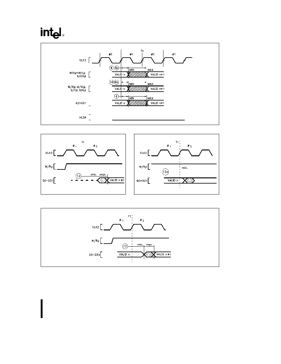
Intel386
TM
DX MICROPROCESSOR
231630 � 41
Figure 9-5 Output Valid Delay Timing
231630 � 79
231630 � 80
Figure 9-5a Write Data Valid Delay Timing
(25 MHz 33 MHz)
Figure 9-5b Write Data Hold Timing
(25 MHz 33 MHz)
231630 � 81
Figure 9-5c Write Data Valid Delay Timing (20 MHz)
133

Intel386
TM
DX MICROPROCESSOR
9 5 5 Typical Output Valid Delay Versus Load Capacitance
at Maximum Operating Temperature (C
L
e
120 pF)
231630 � 77
NOTE
This graph will not be linear outside of the C
L
range shown
9 5 6 Typical Output Valid Delay Versus Load Capacitance
at Maximum Operating Temperature (C
L
e
75 pF)
231630 � 82
NOTE
This graph will not be linear outside of the C
L
range shown
134

Intel386
TM
DX MICROPROCESSOR
9 5 7 Typical Output Valid Delay Versus Load Capacitance
at Maximum Operating Temperature (C
L
e
50 pF)
231630 � 83
NOTE
This graph will not be linear outside of the C
L
range shown
9 5 8 Typical Output Rise Time Versus Load Capacitance
at Maximum Operating Temperature
231630 � 78
NOTE
This graph will not be linear outside of the C
L
range shown
135
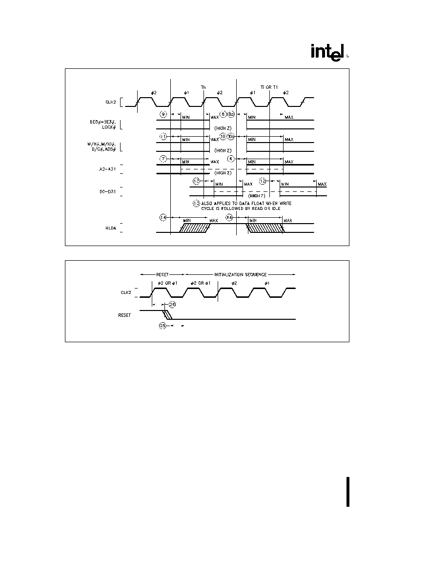
Intel386
TM
DX MICROPROCESSOR
231630 � 42
Figure 9-6 Output Float Delay and HLDA Valid Delay Timing
231630 � 43
The second internal processor phase following RESET high-to-low transition (provided t
25
and t
26
are met) is w2
Figure 9-7 RESET Setup and Hold Timing and Internal Phase
136

Intel386
TM
DX MICROPROCESSOR
10 REVISION HISTORY
This Intel386 DX data sheet version -005 contains updates and improvements to previous versions A revi-
sion summary is listed here for your convenience
The sections significantly revised since version -001 are
2 9 6
Sequence of exception checking table added
2 9 7
Instruction restart revised
2 11 2
TLB testing revised
2 12
Debugging support revised
3 1
LOCK prefix restricted to certain instructions
4 4 3 3
I O privilege level and I O permission bitmap added
Figures 4-15a 4-15b
I O permission bitmap added
4 6 4
Protection and I O permission bitmap revised
4 6 6
Entering and leaving virtual 8086 mode through task switches trap and interrupt
gates and IRET explained
5 6
Self-test signature stored in EAX
5 8
Coprocessor interface description added
5 8 1
Software testing for coprocessor presence added
Table 6-3
PGA package thermal characteristics added
7
Designing for ICE-Intel386 revised
Figures 7-8 7-9 7-10
ICE-Intel386 clearance requirements added
6 2 3 4
Encoding of 32-bit address mode with no ``sib'' byte corrected
The sections significantly revised since version -002 are
Table 2-5
Interrupt vector assignments updated
Figure 4-15a
Bit
map
offset must be less than or equal to DFFFH
Figure 5-28
Intel386 DX outputs remain in their reset state during self-test
5 7
Component and revision identifier history updated
9 4
20 MHz D C specifications added
9 5
16 MHz A C specifications updated 20 MHz A C specifications added
Table 6-1
Clock counts updated
The sections significantly revised since version -003 are
Table 2-6b
Interrupt priorities 2 and 3 interchanged
2 9 8
Double page faults do not raise double fault exception
Figure 4-5
Maximum-sized segments must have segments Base
11 0
e
0
5 4 3 4
BS16
timing corrected
Figures 5-16 5-17
BS16
timing corrected BS16
must not be asserted once NA
has been
5-19 5-22
sampled asserted in the current bus cycle
9 5
16 MHz and 20 MHz A C specifications revised All timing parameters are now
guaranteed at 1 5V test levels The timing parameters have been adjusted to
remain compatible with previous 0 8V 2 0V specifications
137

Intel386
TM
DX MICROPROCESSOR
The sections significantly revised since version -004 are
Chapter 4
25 MHz Clock data included
Table 2-4
Segment Register Selection Rules updated
5 4 4
Interrupt Acknowledge Cycles discussion corrected
Table 5-10
Additional Stepping Information added
Table 9-3
I
CC
values updated
9 5 2
Table for 25 MHz A C Characteristics added A C Characteristics tables reor-
dered
Figure 9-5
Output Valid Delay Timing Figure reconfigured Partial data now provided in addi-
tional Figures 9-5a and 9-5b
Table 6-1
Clock counts updated and formats corrected
The sections significantly revised since version -005 are
Table of Contents
Simplified
Chapter 1
Pin Assignment
2 3 6
Control Register 0
Table 2-4
Segment override prefixes possible
Figure 4-6
Note added
Figure 4-7
Note added
5 2 3
Data bus state at end of cycle
5 2 8 4
Coprocessor error
5 5 3
Bus activity during and following reset
Figure 5-28
ERROR
Chapter 6
Moved forward in datasheet
Chapter 7
Moved forward in datasheet
Chapter 8
Upgraded to chapter
Table 9-3
25 MHz I
CC
Typ value corrected
Table 9-3
33 MHz D C Specifications added
Table 9-4
33 MHz A C Specifications added
Figure 9-5
t8a and t10a added
Figure 9-5c
Added
9 5 6
Added derating for C
L
e
75 pF
9 5 7
Added derating for C
L
e
50 pF
Figure 9 6
t8a and t10a added
The sections significantly revised since version -006 are
2 3 4
Alignment of maximum sized segments
2 9 8
Double page faults do not raise double fault exception
5 5 3
ERROR
and BUSY
sampling after RESET
Figure 5-21
BS16
timing altered
Figure 5-26
READY
timing altered
Figure 5-28
ERROR
timing corrected
6 2 3 1
Corrected Encoding of Register Field Chart
Chapter 7
Updated ICE-Intel386 DX information
9 5 2
Remove preliminary stamp on 25 MHz A C Specifications
9 5 2
Remove preliminary stamp on 33 MHz A C Specifications
138

Intel386
TM
DX MICROPROCESSOR
The sections significantly revised since version -007 are
Table of Contents
Page numbers revised
Figure 5-15
BS16
timing altered
Figure 5-22
Previous cycle T2 changed to Idle cycle Ti
6 1
Note about wait states added
Table 6-1
Opcodes for AND OR and XOR instructions corrected
Table 6-1
Bits 3 4 and 5 of the ``mod r m'' byte corrected for the LTR instruction
Table 8-2
Reference to Figure 6-4 should be reference Figure 8-2
Table 8-2
Note
4 added
The sections significantly revised since version -008 are
Table 9-3
20 25 33 MHz I
CC
specifications updated
139