Äîêóìåíòàöèÿ è îïèñàíèÿ www.docs.chipfind.ru
Wireless Components
ASK Single Conversion Receiver
TDA 5200 Version 2.7
Specification March 2000

Edition 03.00
Published by Infineon Technologies AG,
Balanstraße 73,
81541 München
©
Infineon Technologies AG March 2000.
All Rights Reserved.
Attention please!
As far as patents or other rights of third parties are concerned, liability is only assumed for components, not for applications, processes and circuits im-
plemented within components or assemblies.
The information describes the type of component and shall not be considered as assured characteristics.
Terms of delivery and rights to change design reserved.
Due to technical requirements components may contain dangerous substances. For information on the types in question please contact your nearest
Infineon Technologies Office.
Infineon Technologies AG is an approved CECC manufacturer.
Packing
Please use the recycling operators known to you. We can also help you get in touch with your nearest sales office. By agreement we will take packing
material back, if it is sorted. You must bear the costs of transport.
For packing material that is returned to us unsorted or which we are not obliged to accept, we shall have to invoice you for any costs incurred.
Components used in life-support devices or systems must be expressly authorized for such purpose!
Critical components
1
of the Infineon Technologies AG, may only be used in life-support devices or systems
2
with the express written approval of the
Infineon Technologies AG.
1 A critical component is a component used in a life-support device or system whose failure can reasonably be expected to cause the failure of that life-
support device or system, or to affect its safety or effectiveness of that device or system.
2 Life support devices or systems are intended (a) to be implanted in the human body, or (b) to support and/or maintain and sustain human life. If they
fail, it is reasonable to assume that the health of the user may be endangered.
ABM
®
, AOP
®
, ARCOFI
®
, ARCOFI
®
-BA, ARCOFI
®
-SP, DigiTape
®
, EPIC
®
-1, EPIC
®
-S, ELIC
®
, FALC
®
54, FALC
®
56, FALC
®
-E1, FALC
®
-LH, IDEC
®
, IOM
®
,
IOM
®
-1, IOM
®
-2, IPAT
®
-2, ISAC
®
-P, ISAC
®
-S, ISAC
®
-S TE, ISAC
®
-P TE, ITAC
®
, IWE
®
, MUSAC
®
-A, OCTAT
®
-P, QUAT
®
-S, SICAT
®
, SICOFI
®
, SICOFI
®
-
2, SICOFI
®
-4, SICOFI
®
-4µC, SLICOFI
®
are registered trademarks of Infineon Technologies AG.
ACE
TM
, ASM
TM
, ASP
TM
, POTSWIRE
TM
, QuadFALC
TM
, SCOUT
TM
are trademarks of Infineon Technologies AG.
Revision History
Current Version: 2.7 as of 07.03.2000
Previous Version: 2.6, November 1999
Page
(in previous
Version)
Page
(in current
Version)
Subjects (major changes since last revision)
Product Info
Product Info
Wireless Components
Specification, March 2000
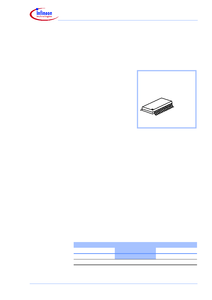
Package
TDA 5200
Product Info
General Description
The IC is a very low power consump-
tion single chip ASK Single Conver-
sion Receiver for the frequency bands
868-870 MHz and 433-435 MHz. The
IC offers a high level of integration and
needs only a few external compo-
nents. The device contains a low noise
amplifier (LNA), a double balanced
mixer, a fully integrated VCO, a PLL
synthesiser, a crystal oscillator, a lim-
iter with RSSI generator, a data filter, a
data comparator (slicer) and a peak
detector. Additionally there is a power
down feature to save battery life.
Features
Low supply current (I
s
= 4.8mA typ.
at 868MHz, I
s
= 4.6mA typ. at
434MHz)
Supply voltage range 5V ±10%
Power down mode with very low
supply current (50nA typ)
Fully integrated VCO and PLL
Synthesiser
RF input sensitivity < 107dBm
Selectable frequency ranges
868-870 MHz and 433-435 MHz
Limiter with RSSI generation,
operating at 10.7MHz
Selectable reference frequency
2nd order low pass data filter with
external capacitors
Data slicer with self-adjusting
threshold
Application
Keyless Entry Systems
Remote Control Systems
Alarm Systems
Low Bitrate Communication
Systems
Ordering Information
Type
Ordering Code
Package
TDA 5200
Q67037-A1049 P-TSSOP-28-1
available on tape and reel

1
Table of Contents
1 Table of Contents . . . . . . . . . . . . . . . . . . . . . . . . . . . . . . . . . . . . . . . . . . . . . . . . . . . . . . . . . . . .
i
2 Product Description . . . . . . . . . . . . . . . . . . . . . . . . . . . . . . . . . . . . . . . . . . . . . . . . . . . . . . . . . .
2-1
2.1
Overview. . . . . . . . . . . . . . . . . . . . . . . . . . . . . . . . . . . . . . . . . . . . . . . . . . . . . . . . . . . . . . .
2-2
2.2
Application . . . . . . . . . . . . . . . . . . . . . . . . . . . . . . . . . . . . . . . . . . . . . . . . . . . . . . . . . . . . .
2-2
2.3
Features . . . . . . . . . . . . . . . . . . . . . . . . . . . . . . . . . . . . . . . . . . . . . . . . . . . . . . . . . . . . . . .
2-2
2.4
Package Outlines . . . . . . . . . . . . . . . . . . . . . . . . . . . . . . . . . . . . . . . . . . . . . . . . . . . . . . . .
2-3
3 Functional Description . . . . . . . . . . . . . . . . . . . . . . . . . . . . . . . . . . . . . . . . . . . . . . . . . . . . . . . .
3-1
3.1
Pin Configuration . . . . . . . . . . . . . . . . . . . . . . . . . . . . . . . . . . . . . . . . . . . . . . . . . . . . . . . .
3-2
3.2
Pin Definition and Function. . . . . . . . . . . . . . . . . . . . . . . . . . . . . . . . . . . . . . . . . . . . . . . . .
3-3
3.3
Functional Block Diagram. . . . . . . . . . . . . . . . . . . . . . . . . . . . . . . . . . . . . . . . . . . . . . . . . .
3-9
3.4
Functional Blocks . . . . . . . . . . . . . . . . . . . . . . . . . . . . . . . . . . . . . . . . . . . . . . . . . . . . . . . .
3-10
3.4.1 Low Noise Amplifier (LNA) . . . . . . . . . . . . . . . . . . . . . . . . . . . . . . . . . . . . . . . . . . . . . . . . .
3-10
3.4.2 Mixer. . . . . . . . . . . . . . . . . . . . . . . . . . . . . . . . . . . . . . . . . . . . . . . . . . . . . . . . . . . . . . . . . .
3-10
3.4.3 PLL Synthesizer . . . . . . . . . . . . . . . . . . . . . . . . . . . . . . . . . . . . . . . . . . . . . . . . . . . . . . . . .
3-10
3.4.4 Crystal Oscillator . . . . . . . . . . . . . . . . . . . . . . . . . . . . . . . . . . . . . . . . . . . . . . . . . . . . . . . .
3-11
3.4.5 Limiter. . . . . . . . . . . . . . . . . . . . . . . . . . . . . . . . . . . . . . . . . . . . . . . . . . . . . . . . . . . . . . . . .
3-11
3.4.6 Data Filter . . . . . . . . . . . . . . . . . . . . . . . . . . . . . . . . . . . . . . . . . . . . . . . . . . . . . . . . . . . . . .
3-11
3.4.7 Data Slicer . . . . . . . . . . . . . . . . . . . . . . . . . . . . . . . . . . . . . . . . . . . . . . . . . . . . . . . . . . . . .
3-12
3.4.8 Peak Detector. . . . . . . . . . . . . . . . . . . . . . . . . . . . . . . . . . . . . . . . . . . . . . . . . . . . . . . . . . .
3-12
3.4.9 Bandgap Reference Circuitry . . . . . . . . . . . . . . . . . . . . . . . . . . . . . . . . . . . . . . . . . . . . . . .
3-12
4 Applications . . . . . . . . . . . . . . . . . . . . . . . . . . . . . . . . . . . . . . . . . . . . . . . . . . . . . . . . . . . . . . . . .
4-1
4.1
Choice of LNA Threshold Voltage and Time Constant. . . . . . . . . . . . . . . . . . . . . . . . . . . .
4-2

4.2
Data Filter Design. . . . . . . . . . . . . . . . . . . . . . . . . . . . . . . . . . . . . . . . . . . . . . . . . . . . . . . .
4-4
4.3
Quartz Load Capacitance Calculation . . . . . . . . . . . . . . . . . . . . . . . . . . . . . . . . . . . . . . . .
4-5
4.4
Quartz Frequency Calculation . . . . . . . . . . . . . . . . . . . . . . . . . . . . . . . . . . . . . . . . . . . . . .
4-6
4.5
Data Slicer Threshold Generation . . . . . . . . . . . . . . . . . . . . . . . . . . . . . . . . . . . . . . . . . . .
4-7
5 Reference . . . . . . . . . . . . . . . . . . . . . . . . . . . . . . . . . . . . . . . . . . . . . . . . . . . . . . . . . . . . . . . . . . .
5-1
5.1
Electrical Data . . . . . . . . . . . . . . . . . . . . . . . . . . . . . . . . . . . . . . . . . . . . . . . . . . . . . . . . . .
5-2
5.1.1 Absolute Maximum Ratings . . . . . . . . . . . . . . . . . . . . . . . . . . . . . . . . . . . . . . . . . . . . . . . .
5-2
5.1.2 Operating Range . . . . . . . . . . . . . . . . . . . . . . . . . . . . . . . . . . . . . . . . . . . . . . . . . . . . . . . .
5-3
5.1.3 AC/DC Characteristics . . . . . . . . . . . . . . . . . . . . . . . . . . . . . . . . . . . . . . . . . . . . . . . . . . . .
5-4
5.2
Test Circuit . . . . . . . . . . . . . . . . . . . . . . . . . . . . . . . . . . . . . . . . . . . . . . . . . . . . . . . . . . . . .
5-9
5.3
Test Board Layouts . . . . . . . . . . . . . . . . . . . . . . . . . . . . . . . . . . . . . . . . . . . . . . . . . . . . . .
5-10
5.4
Bill of Materials . . . . . . . . . . . . . . . . . . . . . . . . . . . . . . . . . . . . . . . . . . . . . . . . . . . . . . . . . .
5-12
Document Outline