
Wireless Components
2 Band TV Tuner Mixer-Oscillator-PLL
with unbalanced IF-Amplifier
KTS6027-2, KTS6029-2 Version 2.0
Specification July 2001

Edition 03.99
Published by Infineon Technologies AG
Balanstra�e 73,
81541 M�nchen
�
Infineon Technologies AG 20.07.01.
All Rights Reserved.
Attention please!
As far as patents or other rights of third parties are concerned, liability is only assumed for components, not for applications, processes and circuits im-
plemented within components or assemblies.
The information describes the type of component and shall not be considered as assured characteristics.
Terms of delivery and rights to change design reserved.
Due to technical requirements components may contain dangerous substances. For information on the types in question please contact your nearest
Infineon Technologies Office.
Infineon Technologies AG is an approved CECC manufacturer.
Packing
Please use the recycling operators known to you. We can also help you � get in touch with your nearest sales office. By agreement we will take packing
material back, if it is sorted. You must bear the costs of transport.
For packing material that is returned to us unsorted or which we are not obliged to accept, we shall have to invoice you for any costs incurred.
Components used in life-support devices or systems must be expressly authorized for such purpose!
Critical components
1
of the Infineon Technologies AG, may only be used in life-support devices or systems
2
with the express written approval of the
Infineon Technologies AG.
1 A critical component is a component used in a life-support device or system whose failure can reasonably be expected to cause the failure of that life-
support device or system, or to affect its safety or effectiveness of that device or system.
2 Life support devices or systems are intended (a) to be implanted in the human body, or (b) to support and/or maintain and sustain human life. If they
fail, it is reasonable to assume that the health of the user may be endangered.
ABM
�
, AOP
�
, ARCOFI
�
, ARCOFI
�
-BA, ARCOFI
�
-SP, DigiTape
�
, EPIC
�
-1, EPIC
�
-S, ELIC
�
, FALC
�
54, FALC
�
56, FALC
�
-E1, FALC
�
-LH, IDEC
�
, IOM
�
,
IOM
�
-1, IOM
�
-2, IPAT
�
-2, ISAC
�
-P, ISAC
�
-S, ISAC
�
-S TE, ISAC
�
-P TE, ITAC
�
, IWE
�
, MUSAC
�
-A, OCTAT
�
-P, QUAT
�
-S, SICAT
�
, SICOFI
�
, SICOFI
�
-
2, SICOFI
�
-4, SICOFI
�
-4�C, SLICOFI
�
are registered trademarks of Infineon Technologies AG.
ACE
TM
, ASM
TM
, ASP
TM
, POTSWIRE
TM
, QuadFALC
TM
, SCOUT
TM
are trademarks of Infineon Technologies AG.
Revision History: Current Version: Preliminary Datasheet V 1.1, July 2000
Previous Version:Target Data Sheet
Page
(in previous
Version)
Page
(in current
Version)
Subjects (major changes since last revision)
all
all
version to 1.1, status to preliminary
4 - 2
4 - 2
circuit diagram modified
4 - 3
4 - 3
circuit diagram modified
5 - 2
5 - 2
Bus input/output SDA max changed to 6V,
Bus input SCL max changed to 6V,
ADC input added
5 - 3
5 - 3
new reference for ESD protection
5 - 5
5 - 5
Current consumption for LOW/MID band and HIGH band added,
tbf's replaced by data
Charge Pump output voltage VCP = 1.3 V min
5 - 8
5 - 8
Oscillator phsase noise -85 dBc/Hz min, -89 dBc/Hz typ
5 - 9
5 - 9
Oscillator phsase noise -85 dBc/Hz min, -89 dBc/Hz typ
Revision History: Current Version: Datasheet, V 2.0, July 2001
Previous Version:Preliminary Datasheet V 1.1, July 2000
Page
(in previous
Version)
Page
(in current
Version)
Subjects (major changes since last revision)
all
all
version to 2.0, preliminary deleted
5 - 2
5- 2
definition of thermal properties changed
5 - 5
5 - 5
current consumtion changed

Product Info
Product Info
Wireless Components
Specification, July 2001
Package
KTS6027-2, KTS6029-2
Product Info
General Description
The KTS6027-2/KTS6029-2 is a 5 V
mixer/oscillator and synthesizer for
analog and digital TV and VCR tuners.
Features
General
s
Suitable for analog and digital ter-
restrial TV tuner
s
Compatible with KTS6027-S or
KTS6029-S in normal mode
s
New features in extended mode
s
Full ESD protection
Mixer/Oscillator
s
High impedance mixer input for
LOW/MID band
s
Low impedance mixer input for
HIGH band
s
4 pin oscillator for LOW/MID band
s
4 pin oscillator for HIGH band
IF-Amplifier
s
single ended IF preamplifier
s
75
output impedance
PLL
s
PLL with short lock-in time
s
High voltage VCO tuning output
s
Fast I
2
C bus
s
4 NPN bandswitch buffers
s
Internal LOW-MID/HIGH switch
s
Lock-in flag
s
Power-down reset
s
4 programmable reference divider
ratios: 24, 64, 80, 128
s
4 programmable charge pump cur-
rents
Application
Ordering Information
Type
Ordering Code
Package
KTS6027-2
Q67037-A1162 ( tape and reel)
P-TSSOP-28-1
KTS6029-2
Q67037-A1163 ( tape and reel)
P-TSSOP-28-1
s
The IC is suitable for NTSC tuners in TV- and VCR-sets or CATV set-top
receivers for analog TV and Digital Video Broadcasting.

1
Table of Contents
1
Table of Contents . . . . . . . . . . . . . . . . . . . . . . . . . . . . . . . . . . . . . . . 1-4
2
Product Description . . . . . . . . . . . . . . . . . . . . . . . . . . . . . . . . . . . . . 2-5
2.1
General Description . . . . . . . . . . . . . . . . . . . . . . . . . . . . . . . . . . . . . . 2-6
2.2
Features . . . . . . . . . . . . . . . . . . . . . . . . . . . . . . . . . . . . . . . . . . . . . . . 2-6
2.3
Application . . . . . . . . . . . . . . . . . . . . . . . . . . . . . . . . . . . . . . . . . . . . . 2-7
2.4
Package Outlines . . . . . . . . . . . . . . . . . . . . . . . . . . . . . . . . . . . . . . . . 2-7
3
Functional Description . . . . . . . . . . . . . . . . . . . . . . . . . . . . . . . . . . . 3-8
3.1
Pin Configuration . . . . . . . . . . . . . . . . . . . . . . . . . . . . . . . . . . . . . . . . 3-9
3.2
Internal Pin Configuration . . . . . . . . . . . . . . . . . . . . . . . . . . . . . . . . . 3-10
3.3
Block Diagram . . . . . . . . . . . . . . . . . . . . . . . . . . . . . . . . . . . . . . . . . 3-15
3.4
Circuit Description. . . . . . . . . . . . . . . . . . . . . . . . . . . . . . . . . . . . . . . 3-16
4
Applications . . . . . . . . . . . . . . . . . . . . . . . . . . . . . . . . . . . . . . . . . . 4-19
4.1
KTS6027-2 Evaluation Board . . . . . . . . . . . . . . . . . . . . . . . . . . . . . . 4-20
4.2
KTS6029-2 Evaluation Board . . . . . . . . . . . . . . . . . . . . . . . . . . . . . . 4-21
5
Reference . . . . . . . . . . . . . . . . . . . . . . . . . . . . . . . . . . . . . . . . . . . . 5-22
5.1
Electrical Data. . . . . . . . . . . . . . . . . . . . . . . . . . . . . . . . . . . . . . . . . . 5-23
5.1.1 Absolute Maximum Ratings . . . . . . . . . . . . . . . . . . . . . . . . . . . . . . . 5-23
5.1.2 Operating Range . . . . . . . . . . . . . . . . . . . . . . . . . . . . . . . . . . . . . . . 5-25
5.1.3 AC/DC Characteristics . . . . . . . . . . . . . . . . . . . . . . . . . . . . . . . . . . . 5-26
5.2
Programming . . . . . . . . . . . . . . . . . . . . . . . . . . . . . . . . . . . . . . . . . . 5-31
5.3
I2C Bus Timing Diagram. . . . . . . . . . . . . . . . . . . . . . . . . . . . . . . . . . 5-35
5.4
Test Circuits . . . . . . . . . . . . . . . . . . . . . . . . . . . . . . . . . . . . . . . . . . . 5-36
5.4.1 Gain (GV) test Set-up in LOW/MID. . . . . . . . . . . . . . . . . . . . . . . . . . 5-36
5.4.2 Gain (GV) test Set-up in HIGH . . . . . . . . . . . . . . . . . . . . . . . . . . . . . 5-36
5.4.3 Matching circuit for optimum noise figure in LOW/MID. . . . . . . . . . . 5-37
5.4.4 Noise Figure Test Set-up in LOW/MID . . . . . . . . . . . . . . . . . . . . . . . 5-37
5.4.5 Noise Figure Test Set-up in HIGH . . . . . . . . . . . . . . . . . . . . . . . . . . 5-38
5.4.6 Cross modulation Test Set-up in LOW/MID band. . . . . . . . . . . . . . . 5-38
5.4.7 Cross modulation Test Set-up in HIGH band . . . . . . . . . . . . . . . . . . 5-39
5.4.8 Measurement of fref and fdiv . . . . . . . . . . . . . . . . . . . . . . . . . . . . . . 5-39
5.5
Electrical Diagrams . . . . . . . . . . . . . . . . . . . . . . . . . . . . . . . . . . . . . . 5-40
5.5.1 Input admittance (S11) of the LOW/MID band mixer input . . . . . . . . 5-40
5.5.2 Input impedance (S11) of the HIGH band mixer input . . . . . . . . . . . 5-40
5.5.3 Output admittance (S22) of the Mixer output . . . . . . . . . . . . . . . . . . 5-41
5.5.4 Output impedance (S22) of the IF output . . . . . . . . . . . . . . . . . . . . . 5-41

2
Product Description
2.1
General Description . . . . . . . . . . . . . . . . . . . . . . . . . . . . . . . . . . . . . . 2-6
2.2
Features . . . . . . . . . . . . . . . . . . . . . . . . . . . . . . . . . . . . . . . . . . . . . . . 2-6
2.3
Application . . . . . . . . . . . . . . . . . . . . . . . . . . . . . . . . . . . . . . . . . . . . . 2-7
2.4
Package Outlines . . . . . . . . . . . . . . . . . . . . . . . . . . . . . . . . . . . . . . . . 2-7
Contents of this Chapter

Product Description
2 - 6
KTS6027-2, KTS6029-2
Wireless Components
Specification, July 2001
2.1
General Description
The KTS6027-2, KTS6029-2 device combines a digitally programmable phase
locked loop (PLL), with a mixer-oscillator block including two balanced mixers
and oscillators for use in TV and VCR tuners.
The PLL block with four selectable chip addresses forms a digitally programm-
able phase locked loop. With a 4 MHz quartz crystal, the PLL permits precise
setting of the frequency of the tuner oscillator up to 1024 MHz in increments of
31.25, 50, 62.5 or 166.7 kHz. The tuning process is controlled by a micropro-
cessor via an I
2
C bus. The device has four output ports. A flag is set when the
loop is locked. It can be read by the processor via the I
2
C bus.
The mixer-oscillator block includes two balanced mixers (one mixer with high-
impedance input and one mixer with a balanced low-impedance input), two fre-
quency and amplitude-stable balanced oscillators for LOW/MID and HIGH, an
IF amplifier, a low-noise reference voltage source, and a band switch.
2.2
Features
General
s
Suitable for analog and digital terrestrial TV tuner
s
Compatible with KTS6027-S or KTS6029-S in normal mode
s
New features in extended mode
s
Full ESD protection
Mixer/Oscillator
s
High impedance mixer input for LOW/MID band
s
Low impedance mixer input for HIGH band
s
4 pin oscillator for LOW/MID band
s
4 pin oscillator for HIGH band
IF-Amplifier
s
single ended IF preamplifier
s
75
output impedance
PLL
s
PLL with short lock-in time
s
High voltage VCO tuning output
s
Fast I
2
C bus
s
4 NPN bandswitch buffers
s
Internal LOW-MID/HIGH switch

Product Description
2 - 7
KTS6027-2, KTS6029-2
Wireless Components
Specification, July 2001
s
Lock-in flag
s
Power-down reset
s
4 programmable reference divider ratios: 24, 64, 80, 128
s
4 programmable charge pump currents
2.3
Application
s
The IC is suitable for NTSC tuners in TV- and VCR-sets or CATV set-top
receivers for analog TV and Digital Video Broadcasting.
2.4
Package Outlines
P-TSSOP-28-1

3
Functional Description
3.1
Pin Configuration . . . . . . . . . . . . . . . . . . . . . . . . . . . . . . . . . . . . . . . . 3-9
3.2
Internal Pin Configuration . . . . . . . . . . . . . . . . . . . . . . . . . . . . . . . . . 3-10
3.3
Block Diagram . . . . . . . . . . . . . . . . . . . . . . . . . . . . . . . . . . . . . . . . . 3-15
3.4
Circuit Description. . . . . . . . . . . . . . . . . . . . . . . . . . . . . . . . . . . . . . . 3-16
3.4.1 General . . . . . . . . . . . . . . . . . . . . . . . . . . . . . . . . . . . . . . . . . . . . . . . 3-16
3.4.2 Mixer-Oscillator block . . . . . . . . . . . . . . . . . . . . . . . . . . . . . . . . . . . . 3-16
3.4.3 PLL block . . . . . . . . . . . . . . . . . . . . . . . . . . . . . . . . . . . . . . . . . . . . . 3-16
3.4.4 I2C-Bus Interface . . . . . . . . . . . . . . . . . . . . . . . . . . . . . . . . . . . . . . . 3-17
Contents of this Chapter

Functional Description
3 - 9
KTS6027-2, KTS6029-2
Wireless Components
Specification, July 2001
3.1
Pin Configuration
KTS6027-2_Pin_config
Figure 3-1
KTS6027-2 Pin Configuration
KTS6029-2_Pin_config
Figure 3-2
KTS6029-2 Pin Configuration
VCC
MIXOUT
SDA
HIGHIN
HIGHIN
LOW/MIDIN
MIXOUT
PLLGND
SCL
AS
XTAL
PFM
PMID
PLOW
OSCHIGHIN
OSCHIGHOUT
OSCHIGHOUT
OSCHIGHIN
OSCLOW/MIDIN
OSCLOW/MIDOUT
RFGND
ADC
IFOUT
PHIGH
VT
CP
1
2
3
4
5
6
7
8
9
10
11
12
13
14
28
27
26
25
24
23
22
21
20
19
18
17
16
15
KTS6027-2
OSCLOW/MIDOUT
OSCLOW/MIDIN
1
2
3
4
5
6
7
8
9
10
11
12
13
14
28
27
26
25
24
23
22
21
20
19
18
17
16
15
KTS6029-2
VCC
MIXOUT
SDA
HIGHIN
HIGHIN
LOW/MIDIN
MIXOUT
PLLGND
SCL
AS
XTAL
PFM
PMID
PLOW
OSCHIGHIN
OSCHIGHOUT
OSCHIGHOUT
OSCHIGHIN
OSCLOW/MIDIN
OSCLOW/MIDOUT
RFGND
ADC
IFOUT
PHIGH
VT
CP
OSCLOW/MIDOUT
OSCLOW/MIDIN

Functional Description
3 - 10
KTS6027-2, KTS6029-2
Wireless Components
Specification, July 2001
3.2
Internal Pin Configuration
Table 3-1 Pin Definition and Function
Pin No.
Symbol
Equivalent I/O-Schematic
Average DC voltage
LOW/MID
HIGH
1
OSCHIGHIN
0.0 V
1.6 V
2
OSC-
HIGHOUT
0.0 V
2.8 V
3
OSC-
HIGHOUT
0.0 V
2.8 V
4
OSCHIGHIN
0.0 V
1.6 V
5
OSCLOW/
MIDIN
1.6 V
0.0 V
6
OSCLOW/
MIDOUT
2.3 V
0.0 V
7
OSCLOW/
MIDOUT
2.3 V
0.0 V
8
OSCLOW/
MIDIN
1.6 V
0.0 V
9
RFGND
analog ground
0.0 V
0.0 V
2
1
3
4
5
6
8
7
Note: Pin designation refers to KTS6027-2. KTS6029-2 has reversed pinning

Functional Description
3 - 11
KTS6027-2, KTS6029-2
Wireless Components
Specification, July 2001
Table 3-1 Pin Definition and Function (continued)
Pin No.
Symbol
Equivalent I/O-Schematic
Average DC voltage
LOW/MID
HIGH
10
ADC
V
ADC
V
ADC
11
IFOUT
2.3 V
2.3 V
12
PHIGH
5.0 V
V
CE
10
11
12
Functional Description
3 - 12
KTS6027-2, KTS6029-2
Wireless Components
Specification, July 2001
Table 3-1 Pin Definition and Function (continued)
Pin No.
Symbol
Equivalent I/O-Schematic
Average DC voltage
LOW/MID
HIGH
13
VT
V
T
V
T
14
CP
2.1 V
2.1 V
15
PLOW
5 V or V
CE
5 V
16
PMID
5 V or V
CE
5 V
17
PFM
5 V or V
CE
5 V or V
CE
18
XTAL
3.0 V
3.0 V
14
13
15
16
17
18

Functional Description
3 - 13
KTS6027-2, KTS6029-2
Wireless Components
Specification, July 2001
Table 3-1 Pin Definition and Function (continued)
Pin No.
Symbol
Equivalent I/O-Schematic
Average DC voltage
LOW/MID
HIGH
19
AS
V
AS
V
AS
20
SCL
n.a.
n.a.
21
SDA
n.a.
n.a.
22
PLLGND
digital ground
0.0 V
0.0 V
19
20
21

Functional Description
3 - 14
KTS6027-2, KTS6029-2
Wireless Components
Specification, July 2001
Table 3-1 Pin Definition and Function (continued)
Pin No.
Symbol
Equivalent I/O-Schematic
Average DC voltage
LOW/MID
HIGH
23
MIXOUT
3.8 V
3.8 V
24
MIXOUT
3.8 V
3.8 V
25
VCC
supply voltage
5.0 V
5.0 V
26
LOW/MIDIN
1.8 V
0.0 V
27
HIGHIN
0.0 V
0.9 V
28
HIGHIN
0.0 V
0.9 V
Oscillator
IF Amp.
24
23
26
27
28

Functional Description
3 - 15
KTS6027-2, KTS6029-2
Wireless Components
Specification, July 2001
3.3
Block Diagram
KTS602729_block_diag
Note: Pin designations in parenthesis refer to KTS6029-2
Figure 3-3
Block Diagram
O
S
C
H
I
G
H
O
U
T
O
S
C
H
I
G
H
I
N
O
S
C
H
I
G
H
O
U
T
RF Input
HIGH
RF Input
LOW/MID
Mixer
HIGH
Mixer
LOW/MID
Oscillator
HIGH
Oscillator
LOW/MID
SAW
Driver
Prog.
Divider
Phase/
Frequency
Comparator
Crystal
Oscillator
Reference
Divider
Ports
I
2
C Bus
O
S
C
L
O
W
/
M
I
D
I
N
O
S
C
H
I
G
H
I
N
O
S
C
L
O
W
/
M
I
D
O
U
T
R
F
G
N
D
A
D
C
P
H
I
G
H
I
F
O
U
T
V
T
C
P
H
I
G
H
I
N
H
I
G
H
I
N
L
O
W
/
M
I
D
I
N
V
C
C
M
I
X
O
U
T
M
I
X
O
U
T
P
L
L
G
N
D
S
D
A
S
C
L
A
S
X
T
A
L
P
F
M
P
M
I
D
P
L
O
W
f
div
FL
O
S
C
L
O
W
/
M
I
D
O
U
T
O
S
C
L
O
W
/
M
I
D
I
N
Lock
Detector
f
ref
V
CC
LOW
or MID
LOW
or MID
HIGH
HIGH
HIGH
ADC
CP,
CM,
OS
Charge
Pump
LOW
or MID
1
2
3
4
5
6
7
8
9
10
11
12
13
14
28
27
26
25
24
23
22
21
20
19
18
17
16
15
(28)
(27)
(26)
(25)
(24)
(23)
(22)
(21)
(20)
(19) (18)
(17)
(16)
(15)
(1)
(2)
(3)
(4)
(5)
(6)
(7)
(8)
(9)
(10)
(11)
(12)
(13)
(14)

Functional Description
3 - 16
KTS6027-2, KTS6029-2
Wireless Components
Specification, July 2001
3.4
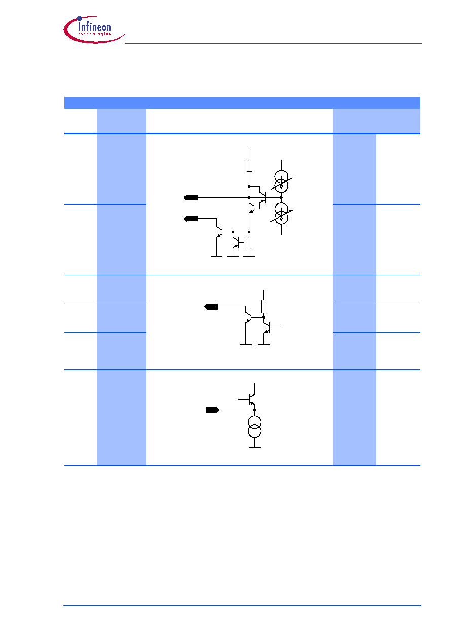
Circuit Description
3.4.1
General
In the normal mode (
see Table 5-7 Test modes on page 32
) the IC is compatible with
KTS6027-S / KTS6029-S. An extended mode makes a reference divider ratio
of 24 (
see Table 5-8 Reference divider ratio on page 32
) and two additional charge pump
currents (
see Table 5-9 Charge pump current on page 33
) available.
3.4.2
Mixer-Oscillator block
The mixer oscillator section includes two balanced mixers (double balanced
mixer), two balanced oscillators for LOW and / or MID band and HIGH band, an
IF amplifier, a reference voltage source and a band switch.
Filters between tuner input and IC separate the TV frequency signals into two
bands. The band switching in the tuner front-end is done by using two or three
port outputs. In the selected band the signal passes a tuner input stage with
MOSFET amplifier, a double-tuned bandpass filter and is then fed to the bal-
anced mixer input of the IC which has in case of LOW / MID a high-impedance
input and in case of HIGH a low-impedance input. The input signal is mixed
there with the signal from the activated on chip oscillator to the IF frequency
which is filtered out at the balanced high-impedance output pair by means of a
parallel tuned circuit. The following SAW preamplifier has a low output imped-
ance to drive the SAW filter directly.
3.4.3
PLL block
The oscillator signal is internally DC-coupled as a differential signal to the pro-
grammable divider inputs. The signal subsequently passes through a program-
mable divider with ratio N = 256 through 32767 and is then compared in a digital
frequency / phase detector to a reference frequency f
ref
= 31.25, 50, 62.5 or
166.7 kHz.
This frequency is derived from an unbalanced, low-impedance 4 MHz crystal
oscillator (pin XTAL) divided by R = 128, 80, 64 or 24.
The phase detector has two outputs that drive two current sources of opposite
polarity as charge pump. If the negative edge of the divided VCO signal appears
prior to the negative edge of the reference signal, the positive current source
pulses for the duration of the phase difference. In the reverse case the negative
current source pulses. If the two signals are in phase, the charge pump output
(CP) goes into the high-impedance state (PLL is locked). An active low-pass fil-
ter integrates the current pulses to generate the tuning voltage for the VCO

Functional Description
3 - 17
KTS6027-2, KTS6029-2
Wireless Components
Specification, July 2001
(internal amplifier, external pull-up resistor at TUNE and external RC circuitry).
The charge pump output is also switched into the high-impedance state if the
control bits T0 = 1 and T1 = 0. Here it should be noted, however, that the tuning
voltage can alter over a long period in the high-impedance state as a result of
self-discharge in the peripheral circuitry. TUNE may be switched off by the con-
trol bit OS to allow external adjustments.
If the VCO is not oscillating the PLL locks to a tuning voltage of 33 V .
By means of the control bits CP, CM, T0 and T1 the pump current can be
switched between four values by software. This programmability permits alter-
ation of the control response time of the PLL in the locked-in state. In this way
different VCO gains can be compensated, for example.
The software-switched ports PLOW, PMID, PHIGH and PFM are general-pur-
pose open-collector outputs. The test bits T0 = 0 and T1 = 1 switches the test
signals f
ref
(i.e.f
XTAL
/ 64) and f
div
(divided input signal) to PLOW and PMID
respectively.
The lock detector resets the lock flag FL if the width of the charge pump current
pulses is wider than the period of the crystal oscillator (i.e. 250 ns). Hence, if FL
= 1, the maximum deviation of the input frequency from the programmed fre-
quency is given by
f =
�
I
P
(K
VCO
/ f
XTAL
) (C1+C2) / (C1C2)
where I
P
is the charge pump current, K
VCO
the VCO gain, f
XTAL
the crystal oscil-
lator frequency and C1, C2 the capacitances in the loop filter (
see Figure 4-1
KTS6027-2 Evaluation Board on page 20
). As the charge pump pulses at i.e. 62.5 kHz (=
f
ref
), it takes a maximum of 16
�
s for FL to be reset after the loop has lost lock
state.
Once FL has been reset, it is set only if the charge pump pulse width is less than
250 ns for eight consecutive f
ref
periods. Therefore it takes between 128 and
144
�
s for FL to be set after the loop regains lock.
3.4.4
I
2
C-Bus Interface
Data is exchanged between the processor and the PLL via the I
2
C bus. The
clock is generated by the processor (input SCL), while pin SDA functions as an
input or output depending on the direction of the data (open collector, external
pull-up resistor). Both inputs have hysteresis and a low-pass characteristic,
which enhance the noise immunity of the I
2
C bus.
The data from the processor pass through an I
2
C bus controller. Depending on
their function the data are subsequently stored in registers. If the bus is free,
both lines will be in the marking state (SDA, SCL are HIGH). Each telegram
begins with the start condition and ends with the stop condition. Start condition:
SDA goes LOW, while SCL remains HIGH. Stop condition: SDA goes HIGH

Functional Description
3 - 18
KTS6027-2, KTS6029-2
Wireless Components
Specification, July 2001
while SCL remains HIGH. All further information transfer takes place during
SCL = LOW, and the data is forwarded to the control logic on the positive clock
edge.
The table "Bit Allocation" (
see Table 5-4 Bit Allocation Read / Write on page 31
) should be
referred to the following description. All telegrams are transmitted byte-by-byte,
followed by a ninth clock pulse, during which the control logic returns the SDA
line to LOW (acknowledge condition). The first byte is comprised of seven
address bits. These are used by the processor to select the PLL from several
peripheral components (chip select). The LSB bit (R/W) determines whether
data are written into (R/W = 0) or read from (R/W = 1) the PLL.
In the data portion of the telegram during a WRITE operation, the MSB bit of the
first or third data byte determines whether a divider ratio or control information
is to follow. In each case the second byte of the same data type has to follow
the first byte.
If the address byte indicates a READ operation, the PLL generates an acknowl-
edge and then shifts out the status byte onto the SDA line. If the processor gen-
erates an acknowledge, a further status byte is output; otherwise the data line
is released to allow the processor to generate a stop condition. The status word
consists the lock flag and the power-on flag.
Four different chip addresses can be set by appropriate DC level at pin AS (
see
Table 5-6 Address selection on page 32
).
While applying the supply voltage, a power-on reset circuit prevents the PLL
from setting the SDA line to LOW, which would block the bus. The power-on
reset flag POR is set at power-on and when V
CC
falls below 3.2 V. It will be reset
at the end of a READ operation.

4
Applications
4.1
KTS6027-2 Evaluation Board . . . . . . . . . . . . . . . . . . . . . . . . . . . . . . 4-20
4.2
KTS6029-2 Evaluation Board . . . . . . . . . . . . . . . . . . . . . . . . . . . . . . 4-21
Contents of this Chapter

Applications
4 - 20
KTS6027-2, KTS6029-2
Wireless Components
Specification, July 2001
4.1
KTS6027-2 Evaluation Board
KTS6027-2 Application Circuit
Figure 4-1
KTS6027-2 Evaluation Board
1p
1p2
1p2
1p2
1p2
2p7
2p2
2p2
2p7
560
33k
L1
L2
L3
120p
BB659C
BA892
1n
1k
3k3
100k
47p
BB659C
2k7
2k7
1k8
1k8
1k
1:1*)
2p2
22p
22p
L4
68p
68p
47n
220
220
4n7
100p
18p
4n7
4n7
4n7
4n7
100p
4n7
4n7
18p
+ 33 V
22k
1n
4 MHz
SDA
SCL
AS
PFM
PMID
PLOW
ADC
HIGH
R
Gen
= 75
LOW/
MID
V
CC
10n
R
Load
= 75
IF
output
100n
220
R
Gen
= 75
1
2
3
4
5
6
7
8
9
10
11
12
13
14
28
27
26
25
24
23
22
21
20
19
18
17
16
15
KTS6027-2
4n7
PHIGH
C
1
2n2
C
2
47n
220
Table 4-1 Recommended band limits in MHz
RF input
Oscillator
min
max
min
max
LOW
55.25
127.25
101
173
MID
133.25
361.25
179
407
HIGH
367.25
803.25
413
849
Table 4-1 Coils
turns
E
wire
E
L1
1.5
2 mm
0.4 mm
L2
3.5
2.5 mm
0.5 mm
L3
9.5
2.5 mm
0.4 mm
L4
12.5
3.5 mm
0.3 mm
*)
TOKO B4F Type 617DB-1023

Applications
4 - 21
KTS6027-2, KTS6029-2
Wireless Components
Specification, July 2001
4.2
KTS6029-2 Evaluation Board
KTS6029-2 Application Circuit
Figure 4-2
KTS6029-2 Evaluation Board
1p
1p2
1p2
1p2
1p2
2p7
2p2
2p2
2p7
C
1
47n
C
2
2n2
560
33k
L1
L2
L3
120p
BB659C
BA892
1n
1k
3k3
100k
47p
BB659C
2k7
2k7
1k8
1k8
1k
1:1*)
2p2
22p
22p
L4
68p
68p
47n
220
220
4n7
100p
18p
4n7
4n7
4n7
4n7
100p
4n7
4n7
18p
+ 33 V
22k
1n
4 MHz
SDA
SCL
AS
PFM
PMID
PLOW
ADC
HIGH
R
Gen
= 75
LOW/
MID
V
CC
10n
R
Load
= 75
IF
output
100n
220
R
Gen
= 75
KTS6029-2
4n7
PHIGH
1
2
3
4
5
6
7
8
9
10
11
12
13
14
28
27
26
25
24
23
22
21
20
19
18
17
16
15
220
Table 4-1 Recommended band limits in MHz
RF input
Oscillator
min
max
min
max
LOW
55.25
127.25
101
173
MID
133.25
361.25
179
407
HIGH
367.25
803.25
413
849
Table 4-1 Coils
turns
E
wire
E
L1
1.5
2 mm
0.4 mm
L2
3.5
2.5 mm
0.5 mm
L3
9.5
2.5 mm
0.4 mm
L4
12.5
3.5 mm
0.3 mm
*)
TOKO B4F Type 617DB-1023

5
Reference
5.1
Electrical Data . . . . . . . . . . . . . . . . . . . . . . . . . . . . . . . . . . . . . . . . . 5-23
5.1.1 Absolute Maximum Ratings . . . . . . . . . . . . . . . . . . . . . . . . . . . . . . . 5-23
5.1.2 Operating Range . . . . . . . . . . . . . . . . . . . . . . . . . . . . . . . . . . . . . . . 5-25
5.1.3 AC/DC Characteristics . . . . . . . . . . . . . . . . . . . . . . . . . . . . . . . . . . . 5-26
5.2
Programming . . . . . . . . . . . . . . . . . . . . . . . . . . . . . . . . . . . . . . . . . 5-31
Table 5-4 Bit Allocation Read / Write . . . . . . . . . . . . . . . . . . . . . . . . . . . . . 5-31
Table 5-5 Description of symbols. . . . . . . . . . . . . . . . . . . . . . . . . . . . . . . . 5-31
Table 5-6 Address selection . . . . . . . . . . . . . . . . . . . . . . . . . . . . . . . . . . . 5-32
Table 5-7 Test modes . . . . . . . . . . . . . . . . . . . . . . . . . . . . . . . . . . . . . . . . 5-32
Table 5-8 Reference divider ratio. . . . . . . . . . . . . . . . . . . . . . . . . . . . . . . . 5-32
Table 5-9 Charge pump current . . . . . . . . . . . . . . . . . . . . . . . . . . . . . . . . . 5-33
Table 5-10 Bandswitching . . . . . . . . . . . . . . . . . . . . . . . . . . . . . . . . . . . . . 5-33
Table 5-11 A/D converter levels. . . . . . . . . . . . . . . . . . . . . . . . . . . . . . . . . 5-34
5.3
I2C Bus Timing Diagram . . . . . . . . . . . . . . . . . . . . . . . . . . . . . . . . 5-35
5.4
Test Circuits . . . . . . . . . . . . . . . . . . . . . . . . . . . . . . . . . . . . . . . . . . 5-36
5.4.1 Gain (GV) test Set-up in LOW/MID. . . . . . . . . . . . . . . . . . . . . . . . . . 5-36
5.4.2 Gain (GV) test Set-up in HIGH . . . . . . . . . . . . . . . . . . . . . . . . . . . . . 5-36
5.4.3 Matching circuit for optimum noise figure in LOW/MID. . . . . . . . . . . 5-37
5.4.4 Noise Figure Test Set-up in LOW/MID . . . . . . . . . . . . . . . . . . . . . . . 5-37
5.4.5 Noise Figure Test Set-up in HIGH . . . . . . . . . . . . . . . . . . . . . . . . . . 5-38
5.4.6 Cross modulation Test Set-up in LOW/MID band. . . . . . . . . . . . . . . 5-38
5.4.7 Cross modulation Test Set-up in HIGH band . . . . . . . . . . . . . . . . . . 5-39
5.4.8 Measurement of fref and fdiv . . . . . . . . . . . . . . . . . . . . . . . . . . . . . . 5-39
5.5
Electrical Diagrams . . . . . . . . . . . . . . . . . . . . . . . . . . . . . . . . . . . . 5-40
5.5.1 Input admittance (S11) of the LOW/MID band mixer input . . . . . . . . 5-40
5.5.2 Input impedance (S11) of the HIGH band mixer input . . . . . . . . . . . 5-40
5.5.3 Output admittance (S22) of the Mixer output . . . . . . . . . . . . . . . . . . 5-41
5.5.4 Output impedance (S22) of the IF output . . . . . . . . . . . . . . . . . . . . . 5-41
Contents of this Chapter

Reference
5 - 23
KTS6027-2, KTS6029-2
Wireless Components
Specification, July 2001
5.1
Electrical Data
5.1.1
Absolute Maximum Ratings
WARNING
The maximum ratings may not be exceeded under any circumstances, not even
momentarily and individually, as permanent damage to the IC may result.
Table 5-1 Absolute Maximum Ratings, Ambient temperature T
AMB
= - 20�C ...T
Amax
Parameter
1).
Symbol
Limit Values
Unit
Remarks
min
max
Supply voltage
V
CC
-0.3
6
V
Ambient temperature
T
A
-10
T
Amax
2).
�
C
Junction temperature
T
J
+125
�
C
Storage temperature
T
Stg
-40
+125
�
C
Temperature difference junction to case
3).
T
JC
2
K
PLL
CP
V
CHGPMP
-0.3
3
V
I
CHGPMP
1
mA
Crystal oscillator pin XTAL
V
XTAL
V
CC
V
I
XTAL
-5
mA
Bus input/output SDA
V
SDA
-0.3
6
V
Bus output current SDA
I
SDA(L)
5
mA
open collector
Bus input SCL
V
SCL
-0.3
6
V
Chip address switch AS
V
AS
-0.3
V
CC
V
VCO tuning output (loop filter)
V
T
-0.3
35
V
ADC inpur
V
ADC
-0.3
V
CC
V
Port outputs PLOW, PMID, PHIGH, PFM
V
P
-0.3
V
CC
V
I
P(L)
-1
25
mA
t
max
= 0.1 sec.
at 5.5 V
Total port output current
I
P(L)
40
mA
t
max
= 0.1 sec.
at 5.5 V

Reference
5 - 24
KTS6027-2, KTS6029-2
Wireless Components
Specification, July 2001
Table 5-1 Absolute Maximum Ratings, Ambient temperature T
AMB
= - 20�C ... + 85�C (continued)
Parameter
1)
Symbol
Limit Values
Unit
Remarks
min
max
Mixer-Oscillator
Mix input LOW/MID
V
i
-0.3
3
V
Mix inputs HIGH
V
i
2
V
I
i
-5
6
mA
VCO base voltage
V
B
-0.3
3
V
VCO collector voltage
V
C
V
CC
V
ESD-Protection
4).
all pins
V
ESD
2
kV
1). All values are referred to ground (pin), unless stated otherwise.
Currents with a positive sign flow into the pin and currents with a negative sign flow out of pin.
2).The maximum ambient temperature depends on the mounting conditions of the package. Any application
mounting must guarantee not to exceed the maximum junction temperature of 125
�
C. As reference the tem-
perature difference junction to case is given.
3).Referred to top center of package
4). According to EIA/JESD22-A114-B (HBM incircuit test), as a single device incircuit contact discharge test.

Reference
5 - 25
KTS6027-2, KTS6029-2
Wireless Components
Specification, July 2001
5.1.2
Operating Range
Within the operational range the IC operates as described in the circuit
description. The AC / DC characteristic limits are not guaranteed.
Table 5-2 Operating Range
Parameter
Symbol
Limit Values
Unit
Test Conditions
L
Item
min
max
Supply voltage
V
CC
+4.5
+5.5
V
Programmable divider factor
N
256
32767
LOW/MID Mixer input frequency
range
f
i
40
500
MHz
HIGH Mixer input frequency
range
f
i
350
900
MHz
LOW/MID Oscillator frequency
range
f
O
75
560
MHz
HIGH Oscillator frequency range
f
O
380
950
MHz
Ambient temperature
T
AMB
-20
T
Amax
1).
�
C
1).
see 5.1.1 Absolute Maximum Ratings on page 23

Reference
5 - 26
KTS6027-2, KTS6029-2
Wireless Components
Specification, July 2001
5.1.3
AC/DC Characteristics
AC / DC characteristics involve the spread of values guaranteed in the specified
supply voltage and ambient temperature range. Typical characteristics are the
median of the production.
Table 5-3 AC/DC Characteristics with T
AMB
= 25 �C, V
CC
Symbol
Limit Values
Unit
Test Conditions
L
Item
min
typ
max
Supply
Supply voltage
V
CC
4.5
5
5.5
V
Current consumption
I
CC
48
61
74
mA
LOW/MID band
51
65
79
mA
HIGH band
Digital Unit
PLL
Crystal oscillator connections XTAL
Crystal frequency
f
XTAL
3.2
4.0
4.8
MHz
series resonance
Crystal resistance
R
XTAL
10
100
series resonance
Oscillation frequency
f
XTAL
3,99975
4,000
4,00025
MHz
f
XTAL
= 4 MHz
Input impedance
Z
XTAL
-700
-900
-1100
f
XTAL
= 4 MHz
Charge pump output CP
Output current,
see Table 5-9 Charge
pump current on page 33
ICPDH
�
430
�
650
�
860
�A
VCP = 1.8 V
ICPH
�
180
� 2
50
�
360
�A
VCP = 1.8 V
ICPDL
�
90
� 1
25
�
180
�A
VCP = 1.8 V
ICPL
�
35
�
50
�
70
�A
VCP = 1.8 V
Tristate current
ICPZ
�
1
nA
T0=1, T1=0
Output voltage
VCP
1.3
2.5
V
PLL locked
Drive output VT (open collector)
HIGH output current
I
TH
10
�A
V
TH
= 33 V, T0 = 1,
T1 = 0
LOW output voltage
V
TL
0.5
V
I
TL
= 1.0 mA
I
2
C-Bus
Bus inputs SCL, SDA
HIGH input voltage
V
IH
3
5.5
V
LOW input voltage
V
IL
0
1.5
V
HIGH input current
I
IH
10
�A
V
IH
= V
CC
LOW input current
I
IL
-10
�A
V
IL
= 0 V

Reference
5 - 27
KTS6027-2, KTS6029-2
Wireless Components
Specification, July 2001
Table 5-3 AC/DC Characteristics with T
AMB
= 25 �C, V
CC
(continued)
Symbol
Limit Values
Unit
Test Conditions
L
Item
min
typ
max
Bus output SDA (open collector)
HIGH output current
I
OH
10
�A
V
OH
= 5.5 V
LOW output voltage
V
OL
0.4
V
I
OL
= 3 mA
Edge speed SCL,SDA
Rise time
t
r
300
ns
Fall time
t
f
300
ns
Clock timing SCL
Frequency
f
SCL
0
400
kHz
HIGH pulse width
t
H
0.6
�s
LOW pulse width
t
L
1.3
�s
Start condition
Set-up time
t
susta
0.6
�s
Hold time
t
hsta
0.6
�s
Stop condition
Set up time
t
susto
0.6
�s
Bus free
t
buf
1.3
�s
Data transfer
Set-up time
t
sudat
0.1
�s
Hold time
t
hdat
0
�s
Input hysteresis
SCL, SDA
V
hys
200
mV
Pulse width of spikes
which are suppressed
t
sp
0
50
ns
Capacitive load for
each bus line
C
L
400
pF
Port outputs PLOW, PMID, PHIGH, PFM (open collector)
HIGH output current
I
POH
1
�A
V
POH
= 5 V
LOW output voltage
V
POL
0.5
V
I
POL
= 25 mA
ADC port input
HIGH input current
I
ADCH
10
�A
LOW input current
I
ADCL
-10
�A
Address selection input AS
HIGH input current
I
ASH
50
�A
V
ASH
= 5 V
LOW input current
I
ASL
-50
�A
V
ASL
= 0 V

Reference
5 - 28
KTS6027-2, KTS6029-2
Wireless Components
Specification, July 2001
Table 5-3 AC/DC Characteristics with T
AMB
= 25 �C, V
CC
(continued)
Symbol
Limit Values
Unit
Test Conditions
L
Item
min
typ
max
Analog Unit
LOW/MID Band Section (including IF amplifier)
Voltage gain
G
V
15
18
21
dB
f
RF
= 55.25 to 361.25
MHz, f
IF
= 41,25 to
58.75 MHz
Mixer noise figure
NF
9
11
dB
f
RF
= 55.25 to 361.25
MHz
Output voltage
causing 0.8 % of
crossmodulation in
channel,
see 5.4.6 on page 38
V
o
109
dB�V
f
RFw
= 55.25 MHz
V
o
109
dB�V
f
RFw
= 361.25 MHz
Input IP2
IP2
140
dB�V
f
RF1
= 55.25 MHz
f
RF2
= 111.00 MHz,
P
RF1
= P
RF2
IP2
135
dB�V
f
RF1
= 361.25 MHz
f
RF2
= 723.00 MHz,
P
RF1
= P
RF2
Input IP3
IP3
110
dB�V
f
RF1
= 55.25 MHz
f
RF2
= 60.75 MHz,
f
RF2
= 61.75 MHz,
P
RF1
= P
RF2
= P
RF3
IP3
110
dB�V
f
RF1
= 253.25 MHz
f
RF2
= 258.75 MHz,
f
RF2
= 259.75 MHz,
P
RF1
= P
RF2
= P
RF3
Output voltage caus-
ing 1 dB compression
Vo
115
dB�V
f
RF
= 55.25 MHz
Vo
115
dB�V
f
RF
= 361.25 MHz
Mixer input
impedance
R
i
0.5
1
1.5
k
parallel equivalent
circuit, f
RF
= 100 MHz
C
i
2
3
pF
parallel equivalent
circuit, f
RF
= 100 MHz
Oscillator frequency
shift, PLL unlocked
f
Osc(V)
400
kHz
V
CC
= 5 V
�
10 %
Oscillator frequency
drift, PLL unlocked
f
Osc(T)
500
kHz
T = 25
�
C
Oscillator frequency
drift, PLL unlocked
f
Osc(t)
100
kHz
t = 5 s up to 15 min
after switching on

Reference
5 - 29
KTS6027-2, KTS6029-2
Wireless Components
Specification, July 2001
Table 5-3 AC/DC Characteristics with T
AMB
= 25 �C, V
CC
(continued)
Symbol
Limit Values
Unit
Test Conditions
L
Item
min
typ
max
Oscillator pulling,
PLL unlocked
V
i
100
108
dB�V
f = 10 kHz
f
RF
= 55.25 MHz
V
i
100
108
dB�V
f = 10 kHz
f
RF
= 361.25 MHz
Oscillator
phase noise
1).
OSC
-86
-89
dBc/Hz
fm = 10kHz
IF suppression
a
IF
15
20
dB
V
i
= 80 dB�V
HIGH Band Section (including IF amplifier)
Voltage gain
G
V
26
29
32
dB
f
RF
= 367.25 MHz to
801.25 MHz,
f
IF
= 41,25 to
58.75 MHz
Mixer noise figure
NF
6
9
dB
f
RF
= 367.25 to
613.25 MHz
7
10
dB
f
RF
= 619.25 to
801.25 MHz
Output voltage
causing 0.8 % of
crossmodulation in
channel,
see 5.4.7 on page 39
V
o
109
dB�V
f
RFw
= 403.25 MHz
V
o
109
dB�V
f
RFw
= 775.25 MHz
Input IP2
IP2
130
dB�V
f
RF1
= 373.25 MHz
f
RF2
= 747.00 MHz,
P
RF1
= P
RF2
Input IP3
IP3
99
dB�V
f
RF1
= 503.25 MHz
f
RF2
= 510.25 MHz,
f
RF2
= 512.25 MHz,
P
RF1
= P
RF2
= P
RF3
IP3
99
dB�V
f
RF1
= 775.25 MHz
f
RF2
= 780.75 MHz,
f
RF2
= 781.75 MHz,
P
RF1
= P
RF2
= P
RF3
Output voltage caus-
ing 1 dB compression
Vo
115
dB�V
f
RF
= 503.25 MHz
Vo
115
dB�V
f
RF
= 799.25 MHz
Mixer input
impedance
R
i
14
20
26
serial equivalent cir-
cuit, f
RF
= 600 MHz
L
i
6
10
14
nH
serial equivalent cir-
cuit, f
RF
= 600 MHz
Oscillator frequency
shift, PLL unlocked
f
Osc(V)
400
kHz
V
CC
= 5 V
�
10 %
Oscillator frequency
drift, PLL unlocked
f
Osc(T)
800
kHz
T = 25
�
C

Reference
5 - 30
KTS6027-2, KTS6029-2
Wireless Components
Specification, July 2001
Table 5-3 AC/DC Characteristics with T
AMB
= 25 �C, V
CC
(continued)
Symbol
Limit Values
Unit
Test Conditions
L
Item
min
typ
max
Oscillator frequency
drift, PLL unlocked
f
Osc(t)
100
kHz
t = 5 s up to 15 min
after switching on
Oscillator pulling,
PLL unlocked
V
i
100
108
dB�V
f = 10 kHz
f
RF
= 367.25 MHz
100
108
dB�V
f = 10 kHz
f
RF
= 801.25 MHz
Oscillator
phase noise
1)
-86
-89
dBc/Hz
fm = 10kHz
IF suppression
a
IF
15
20
dB
V
i
= 80 dB�V
SAW preamplifier
IF output impedance
R
IF
80
serial equivalent
circuit,
f
IF
= 45.75 MHz
L
IF
7
nH
Rejection at the IF outputs
Divider interference
rejection
2).
Vo
30
dB�V
Channel CH6
beat
3).
INT
CH6
70
dBc
V
RFpix
= 80 dB�V
V
RFsnd
= 80 dB�V
Channel A-5 beat
rejection
4).
INT
CHA5
70
dBc
V
RFpix
= 80 dB�V
s
This value is only guaranteed in lab.
1). Measured in the evaluation board. (
see Chapter 4
)
2). This is the level of divider interferences close to the IF frequency. For example channel S3:
fOSC = 158.15 MHz, 1/4 fOSC = 39.5375 MHz. Measured in the evaluation board. (
see Chapter 4
)
3). Channel 6 beat is the interfering product of f
RFpix
+ f
RFsnd
- f
OSC
of channel 6 at 42 MHz. Measured in
the evaluation board. (
see Chapter 4
)
4). Channel A-5 beat is the interfering product of f
RFPIX
+ f
RFSND
- f
OSC
of channel A-5, f
beat
= 45.5 MHz.
The possible mechanisms are f
OSC
- 2 x f
IF
or 2 x f
RFpix
- f
OSC
. Measured in the evaluation board.
(
see Chapter 4
)

Reference
5 - 31
KTS6027-2, KTS6029-2
Wireless Components
Specification, July 2001
5.2
Programming
Table 5-4 Bit Allocation Read / Write
Byte
MSB
bit6
bit5
bit4
bit3
bit2
bit1
LSB
Ack
Write Data
Address Byte
1
1
0
0
0
MA1
MA0
0
A
Progr. Divider
Byte 1
0
N14
N13
N12
N11
N10
N9
N8
A
Progr. Divider
Byte 2
N7
N6
N5
N4
N3
N2
N1
N0
A
Control Byte
1
CP
T1
T0
CM
RSA
RSB
OS
A
Bandswitch
Byte
1).
x
x
x
x
P3
P2
P1 P0 A
Read Data
Address Byte
1
1
0
0
0
MA1
MA0
1
A
Status Byte
POR
FL
x
x
x
A2
A1
A0
A
1).
see Table 5-10 Bandswitching on page 33
Table 5-5 Description of symbols
Symbol
Description
MA0, MA1
Address selection bits (
see Table 5-6 Address selection on page 32
)
N14 to N0
programmable divider bits:
N = 2
14
x N14 + 2
13
x N13 + ..... + 2
3
x N3 + 2
2
x N2 + 2
1
x N1 + N0
CP
charge pump current:
bit = 0: charge pump current = 50 �A
bit = 1: charge pump current = 250�A
T1, T0
test bits (
see Table 5-7 Test modes on page 32
)
CM
charge pump mode bit (
see Table 5-9 Charge pump current on page 33
)
RSA, RSB
reference divider bits (
see Table 5-8 Reference divider ratio on page 32
)
OS
tuning amplifier control bit:
bit = 0: enable V
T
bit = 1: disable V
T
PLOW, PMID, PHIGH,
PFM,
see 5-10 on page 33
NPN ports control bits:
bit = 0: NPN open-collector output is inactive
bit = 1: NPN open-collector output is active
A0, A1, A2
ADC bits (
see Table 5-11 A/D converter levels on page 34
)
FL
PLL lock flag
bit = 1: loop is locked
POR
Power-on reset flag
flag is set at power-on and reset at the end of READ operation
x
don`t care

Reference
5 - 32
KTS6027-2, KTS6029-2
Wireless Components
Specification, July 2001
Table 5-6 Address selection
Voltage at AS
MA1
MA0
(0...0.1) * V
CC
0
0
(0.2...0.3) * VCC or open circuit
0
1
(0.4...0.6) * V
CC
1
0
(0.9...1) * V
CC
1
1
Table 5-7 Test modes
Test mode
Mode
T1
T0
Normal operation
normal
1).
0
0
Charge pump output, CP is in high-impedance state
0
1
PMID = f
div
output, PLOW = fref output
1
0
Extended operation
extended
1
1
1). In this mode the IC is compatible with KTS6027-S / KTS6029-S
Table 5-8 Reference divider ratio
Reference divider ratio
Mode
1).
T1
T0
RSA
RSB
fref
2).
80
normal
0
0
x
0
50 kHz
0
1
1
0
128
0
0
0
1
31.25 kHz
0
1
1
0
64
0
0
1
1
62.5 kHz
0
1
1
0
80
extended
1
1
0
0
50 kHz
128
0
1
31.25 kHz
24
1
0
166.7 kHz
64
1
1
62.5 kHz
1).
see Table 5-7 Test modes on page 32
2). With a 4 MHz quartz.

Reference
5 - 33
KTS6027-2, KTS6029-2
Wireless Components
Specification, July 2001
Table 5-9 Charge pump current
Charge pump current
Mode
1).
CP
T1
T0
CM
50 �A
normal
0
0
0
x
250 �A
1
x
50 �A
extended
0
1
1
0
125 �A
0
1
250 �A
1
0
600 �A
1
1
1).
see Table 5-7 Test modes on page 32
Table 5-10 Bandswitching
Bit Designation
P3
P2
P1
P0
Active Port
Pin
PHIGH
1).
12
0
0
0
0
PLOW
15
0
0
0
1
PMID
16
0
0
1
0
not used
0
0
1
1
PHIGH
12
0
1
0
0
PLOW, PFM
15, 17
0
1
0
1
PMID, PFM
16, 17
0
1
1
0
not used
0
1
1
1
PHIGH
12
1
0
0
0
PLOW, PFM
15, 17
1
0
0
1
PMID, PFM
16, 17
1
0
1
0
not used
1
0
1
1
PHIGH, PFM
12, 17
1
1
0
0
PLOW, PFM
15, 17
1
1
0
1
PMID, PFM
16, 17
1
1
1
0
not used
1
1
1
1
1). Default after power-on

Reference
5 - 34
KTS6027-2, KTS6029-2
Wireless Components
Specification, July 2001
Table 5-11 A/D converter levels
Voltage at ADC
A2
A1
A0
(0...0.15)*V
CC
0
0
0
(0.15...0.3)*V
CC
0
0
1
(0.3...0.45)*V
CC
0
1
0
(0.45...0.6)*V
CC
0
1
1
(0.6...1)*V
CC
1
0
0

Refer
e
n
c
e
5 -
35
K
T
S
602
7-2, K
T
S
6029-
2
W
i
r
e
l
e
ss Com
pone
nt
s
Sp
eci
f
i
c
at
i
on,
J
u
l
y
20
01
5.3
I
2
C
B
u
s
Ti
mi
ng
D
i
a
g
r
a
m
Telegram examples:
Start-ADB-DB1-DB2-CB-BB-Stop
Start-ADB-CB-BB-DB1-DB2-Stop
Start-ADB-DB1-DB2-Stop
Start-ADB-CB-BB-Stop
Abbreviations:
Start= start condition
ADB= address byte
DB1= prog. divider byte 1
DB2= prog. divider byte 2
CB= Control byte
BB= Bandswitch byte
Stop= stop condition
MA1
R/W
MA0
Ack.
Ack.
2nd Byte
1st Byte
3rd Byte
Ack.
Ack.
Ack.
Addressing
4th Byte
1
1
Start
Stop
0
0
0

Reference
5 - 36
KTS6027-2, KTS6029-2
Wireless Components
Specification, July 2001
5.4
Test Circuits
5.4.1
Gain (G
V
) test Set-up in LOW/MID
GVHFM
s
Z
i
>> 50
=> V
i
= 2 x V
meas
= 80 dB�V
s
V
i
= V
meas
+ 6dB = 80 dB�V
s
G
v
= 20 log(V
0
/ V
i
)
5.4.2
Gain (G
V
) test Set-up in HIGH
GUHFM
s
V
i
= V
meas
= 70 dB�V
s
G
v
= 20 log(V
0
/ V
i
) + 1 dB (1 dB = insertion loss of balun)
Device
under
Test
IFOUT
LOW/
MIDIN
V
i
50
50
V
V
meas
RMS
Votmeter
50
spectrum
analyser
V
o
Device
under
Test
IFOUT
HIGHIN
V
i
50
50
V
V
meas
RMS
Votmeter
Balun
1:1
HIGHIN
50
spectrum
analyser
V
o

Reference
5 - 37
KTS6027-2, KTS6029-2
Wireless Components
Specification, July 2001
5.4.3
Matching circuit for optimum noise figure in LOW/MID
NFM
5.4.4
Noise Figure Test Set-up in LOW/MID
NFVHFM
22p
22p
7 turns
wire 0.5 mm
coil 5.5 mm
1n
In
Out
15p
22p
1n
50
semi rigid cable
300 mm long
96 pF/m
33dB/100m
In
Out
For f
RF
= 150 MHz
s
loss = 1.3 dB
s
image suppression = 13 dB
For f
RF
= 50 MHz
s
loss = 0 dB
s
image suppression = 16 dB
Device
under
Test
IFOUT
LOW/
MIDIN
Noise
Source
NF = NFmeas - loss of matching circuit (dB)
Matching
Circuit
IN
OUT
Noise
Figure
Meter

Reference
5 - 38
KTS6027-2, KTS6029-2
Wireless Components
Specification, July 2001
5.4.5
Noise Figure Test Set-up in HIGH
NFUHFM
5.4.6
Cross modulation Test Set-up in LOW/MID band
XVHFM
s
Z
i
>> 50
=> V
i
= 2 x V
meas
s
wanted output signal at f
pix
, V
o
= 100 dB�V
s
unwanted output signal at f
snd
, 80 % AM modulated with 1 kHz
Device
under
Test
IFOUT
HIGHIN
HIGHIN
Balun
1:1
Noise
Source
loss of balun = 1 dB
NF = NFmeas - loss of balun (dB)
Noise
Figure
Meter
Hybrid
A
B
C
D
Device
under
Test
IFOUT
LOW/
MIDIN
V
i
50
50
50
unwanted
signal
source
AM = 80 %
wanted
signal
source
50
V
V
meas
RMS
Votmeter
V
o
45.75 MHz
50
modulation
analyser
18 dB
attenuator

Reference
5 - 39
KTS6027-2, KTS6029-2
Wireless Components
Specification, July 2001
5.4.7
Cross modulation Test Set-up in HIGH band
XUHFM
s
wanted output signal at f
pix
, V
o
= 100 dB�V
s
unwanted output signal at f
snd
, 80 % AM modulated with 1 kHz
5.4.8
Measurement of f
ref
and f
div
MEAS_COF
Hybrid
A
B
C
D
Device
under
Test
IFOUT
HIGHIN
HIGHIN
Balun
1:1
V
i
50
50
50
unwanted
signal
source
AM = 80 %
wanted
signal
source
50
V
V
meas
RMS
Votmeter
V
o
45.75 MHz
50
modulation
analyser
18 dB
attenuator
5k
5k
18p
D
evice under
Test
V
VCC
Counter
Counter
+ 5 V
4 MHz
PMID
PLOW
Test Mode: T1 = 1, T0 = 0
f
Q
= f
ref
* R
R: reference divider ratio
f
VCO
= f
div
* N
N: divider ratio
f
ref
f
div

Reference
5 - 40
KTS6027-2, KTS6029-2
Wireless Components
Specification, July 2001
5.5
Electrical Diagrams
5.5.1
Input admittance (S11) of the LOW/MID band mixer input
Y
0
= 20mS
Y_VHFMIX
5.5.2
Input impedance (S11) of the HIGH band mixer input
Z
0
= 50
(symmetrical)
Zn_UHFMIX
0.1
0.2
0.3
0.4
0.5
0.6
0.7
0.8
0.9
1
1.5
2
3
4
5
10
20
0
0.1
0.1
0.2
0.2
0.3
0.3
0.4
0.4
0.5
0.5
0.6
0.6
0.7
0.7
0.
8
0.
8
0
.9
0
.9
1
1
1.5
1.5
2
2
3
3
4
4
5
5
10
10
20
20
48.25 MHz
407.25 MHz
5
10
15
20
25
30
35
40
45
50
75
100
150
200
250
500
1k
0
5
5
10
10
15
15
20
20
25
25
30
30
35
35
40
40
4
5
4
5
50
50
75
75
100
100
150
150
200
200
250
250
500
500
1k
1k
Rdiff
415.25 MHz
855.25 MHz

Reference
5 - 41
KTS6027-2, KTS6029-2
Wireless Components
Specification, July 2001
5.5.3
Output admittance (S22) of the Mixer output
Y
0
= 20mS
Y_MIXOUT
5.5.4
Output impedance (S22) of the IF output
Z
0
= 50
UIFOUT
0.1
0.2
0.3
0.4
0.5
0.6
0.7
0.8
0.9
1
1.5
2
3
4
5
10
20
0
0.1
0.1
0.2
0.2
0.3
0.3
0.4
0.4
0.5
0.5
0.6
0.6
0.7
0.7
0.
8
0.
8
0
.9
0
.9
1
1
1.5
1.5
2
2
3
3
4
4
5
5
10
10
20
20
Rdiff
45.75 MHz
0.1
0.2
0.3
0.4
0.5
0.6
0.7
0.8
0.9
1
1.5
2
3
4
5
10
20
0
0.1
0.1
0.2
0.2
0.3
0.3
0.4
0.4
0.5
0.5
0.6
0.6
0.7
0.7
0.
8
0.
8
0
.9
0
.9
1
1
1.5
1.5
2
2
3
3
4
4
5
5
10
10
20
20
45.75 MHz