Äîêóìåíòàöèÿ è îïèñàíèÿ www.docs.chipfind.ru

1
2001 Integrated Device Technology, Inc.
DSC-4512/1
APRIL 2001
3.3 VOLT CMOS SuperSync FIFOTM
32,768 X 18
65,536 X 18
IDT72V275
IDT72V285
COMMERCIAL AND INDUSTRIAL TEMPERATURE RANGES
SuperSyncFIFO is a trademark and the IDT logo is a registered trademark of Integrated Device Technology, Inc.
.EATURES:
·
·
·
·
·
Choose among the following memory organizations:
IDT72V275
32,768 x 18
IDT72V285
65,536 x 18
·
·
·
·
·
Pin-compatible with the IDT72V255/72V265 SuperSync FIFOs
·
·
·
·
·
10ns read/write cycle time (6.5ns access time)
·
·
·
·
·
Fixed, low first word data latency time
·
·
·
·
·
Auto power down minimizes standby power consumption
·
·
·
·
·
Master Reset clears entire FIFO
·
·
·
·
·
Partial Reset clears data, but retains programmable
settings
·
·
·
·
·
Retransmit operation with fixed, low first word data
latency time
·
·
·
·
·
Empty, Full and Half-Full flags signal FIFO status
·
·
·
·
·
Programmable Almost-Empty and Almost-Full flags, each flag can
default to one of two preselected offsets
·
·
·
·
·
Program partial flags by either serial or parallel means
·
·
·
·
·
Select IDT Standard timing (using
EF
EF
EF
EF
EF and FF
FF
FF
FF
FF flags) or First Word
Fall Through timing (using
OR
OR
OR
OR
OR and IR
IR
IR
IR
IR flags)
·
·
·
·
·
Output enable puts data outputs into high impedance state
·
·
·
·
·
Easily expandable in depth and width
·
·
·
·
·
Independent Read and Write clocks (permit reading and writing
simultaneously)
·
·
·
·
·
Available in the 64-pin Thin Quad Flat Pack (TQFP) and the 64-pin
Slim Thin Quad Flat Pack (STQFP)
·
·
·
·
·
High-performance submicron CMOS technology
·
·
·
·
·
Industrial temperature range (-40°C to +85°C) is available
DESCRIPTION:
The IDT72V275/72V285 are exceptionally deep, high speed, CMOS
First-In-First-Out (FIFO) memories with clocked read and write controls.
These FIFOs offer numerous improvements over previous SuperSync
FIFOs, including the following:
·
The limitation of the frequency of one clock input with respect to the other
has been removed. The Frequency Select pin (FS) has been removed,
thus it is no longer necessary to select which of the two clock inputs, RCLK
or WCLK, is running at the higher frequency.
·
The period required by the retransmit operation is now fixed and short.
·
The first word data latency period, from the time the first word is written to
an empty FIFO to the time it can be read, is now fixed and short. (The
variable clock cycle counting delay associated with the latency period
found on previous SuperSync devices has been eliminated on this
SuperSync family.)
SuperSync FIFOs are particularly appropriate for network, video, telecom-
munications, data communications and other applications that need to buffer
large amounts of data.
.UNCTIONAL BLOCK DIAGRAM
INPUT REGISTER
OUTPUT REGISTER
RAM ARRAY
32,768 x 18
65,536 x 18
FLAG
LOGIC
FF
/
IR
PAF
EF
/
OR
PAE
HF
READ POINTER
READ
CONTROL
LOGIC
WRITE CONTROL
LOGIC
WRITE POINTER
RESET
LOGIC
WEN
WCLK
D
0
-D
17
LD
MRS
REN
RCLK
OE
Q
0
-Q
17
OFFSET REGISTER
PRS
FWFT/SI
SEN
RT
4512 drw 01
2
COMMERCIAL AND INDUSTRIAL TEMPERATURE RANGE
IDT72V275/72V285
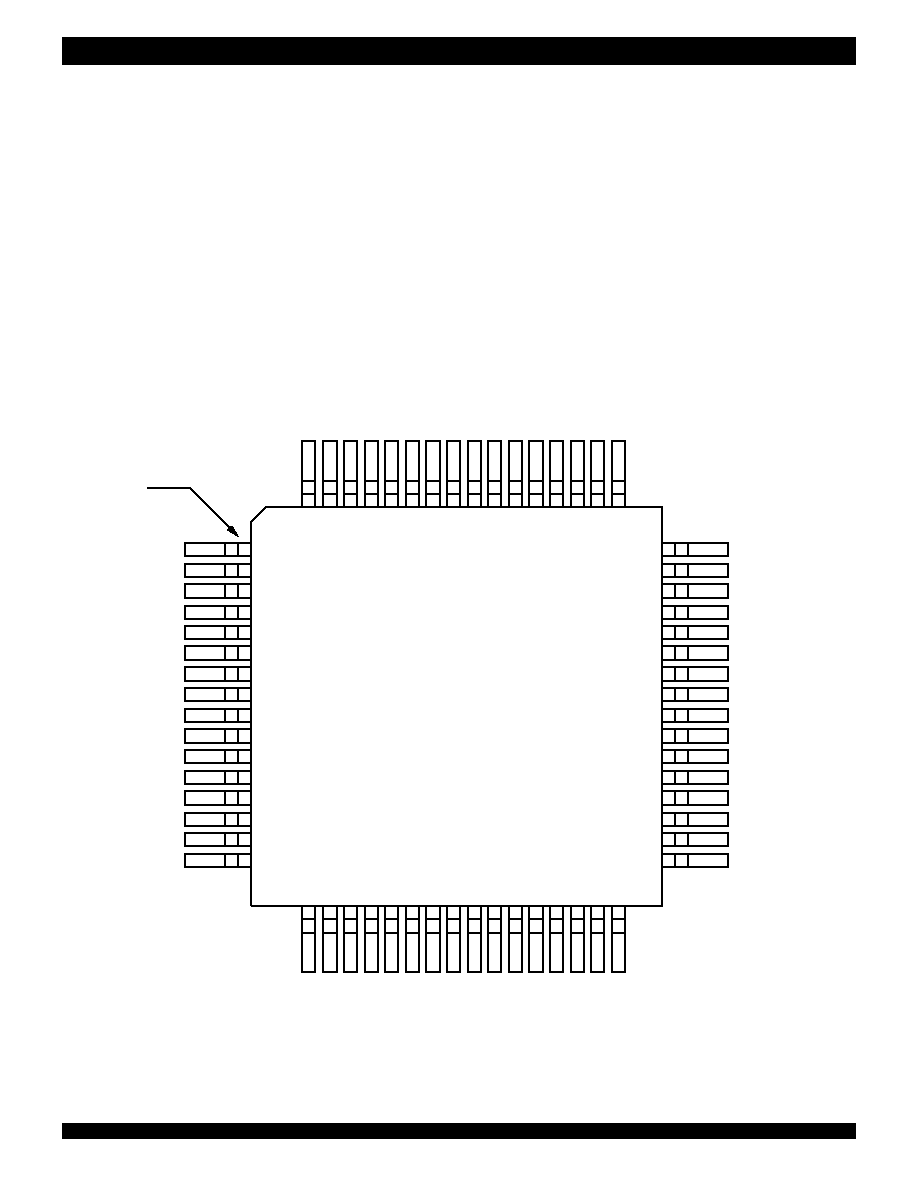
PIN CON.IGURATIONS
TQFP (PN64-1, order code: PF)
STQFP (PP64-1, order code: TF)
TOP VIEW
DESCRIPTION (Continued)
PIN 1
1
2
3
4
5
6
7
8
9
10
11
12
13
14
15
16
48
47
46
45
44
43
42
41
40
39
38
37
36
35
34
33
WEN
SEN
DC
(1)
V
CC
GND
D17
D16
D15
D14
D13
D12
D11
D10
D9
D8
D7
64 63 62 61 60 59 58 57 56 55 54 53 52 51 50 49
17 18 19 20 21 22 23 24 25 26 27 28 29 30 31 32
Q17
Q16
GND
Q15
Q14
V
CC
Q13
Q12
Q11
GND
Q10
Q9
Q8
Q7
Q6
GND
WCLK
PRS
MRS
LD
FWFT/SI
GND
FF
/
IR
PAF
HF
V
CC
PAE
EF
/
OR
RCLK
REN
RT
OE
Q5
Q4
V
CC
Q3
Q2
GND
Q1
Q0
GND
D0
D1
D2
D3
D4
D5
D6
4512 drw 02
The input port is controlled by a Write Clock (WCLK) input and a Write Enable
(
WEN) input. Data is written into the FIFO on every rising edge of WCLK when
WEN is asserted. The output port is controlled by a Read Clock (RCLK) input
and Read Enable (
REN) input. Data is read from the FIFO on every rising
edge of RCLK when
REN is asserted. An Output Enable (OE) input is provided
for three-state control of the outputs.
The frequencies of both the RCLK and the WCLK signals may vary from 0
to f
MAX
with complete independence. There are no restrictions on the frequency
of the one clock input with respect to the other.
There are two possible timing modes of operation with these devices: IDT
Standard mode and First Word Fall Through (FWFT) mode.
In IDT Standard mode, the first word written to an empty FIFO will not appear
on the data output lines unless a specific read operation is performed. A read
operation, which consists of activating
REN and enabling a rising RCLK edge,
will shift the word from internal memory to the data output lines.
In FWFT mode, the first word written to an empty FIFO is clocked directly
to the data output lines after three transitions of the RCLK signal. A
REN does
not have to be asserted for accessing the first word. However, subsequent
words written to the FIFO do require a LOW on
REN for access. The state of
the FWFT/SI input during Master Reset determines the timing mode in use.
For applications requiring more data storage capacity than a single FIFO
can provide, the FWFT timing mode permits depth expansion by chaining FIFOs
in series (i.e. the data outputs of one FIFO are connected to the corresponding
data inputs of the next). No external logic is required.
NOTE:
1. DC = Don't Care. Must be tied to GND or V
CC
, cannot be left open.
3
COMMERCIAL AND INDUSTRIAL TEMPERATURE RANGE
IDT72V275/72V285
DESCRIPTION (Continued)
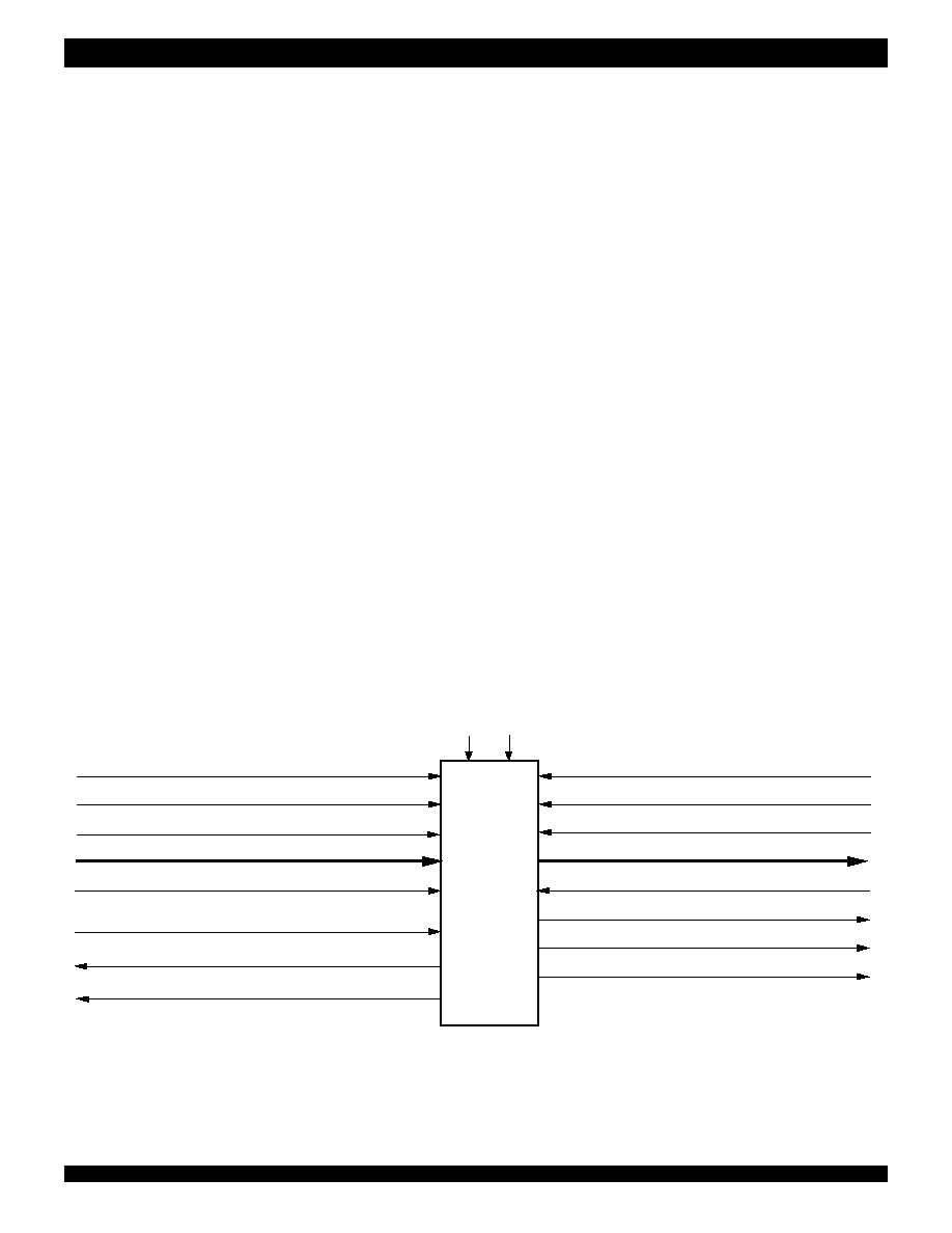
Figure 1. Block Diagram of Single 32,768 x 18 and 65,536 x 18 Synchronous FIFO
DATA OUT (Q
0
- Q
n
)
DATA IN (D
0
- D
n
)
MASTER RESET (
MRS
)
READ CLOCK (RCLK)
READ ENABLE (
REN
)
OUTPUT ENABLE (
OE
)
EMPTY FLAG/OUTPUT READY (
EF
/
OR
)
PROGRAMMABLE ALMOST-EMPTY (
PAE
)
WRITE CLOCK (WCLK)
WRITE ENABLE (
WEN
)
LOAD (
LD
)
FULL FLAG/INPUT READY (
FF
/
IR
)
PROGRAMMABLE ALMOST-FULL (
PAF
)
IDT
72V275
72V285
PARTIAL RESET (
PRS
)
FIRST WORD FALL THROUGH/SERIAL INPUT
(FWFT/SI)
RETRANSMIT (
RT
)
4512 drw 03
HALF-FULL FLAG (
HF
)
SERIAL ENABLE(
SEN
)
These FIFOs have five flag pins,
EF/OR (Empty Flag or Output Ready),
FF/IR (Full Flag or Input Ready), HF (Half-full Flag), PAE (Programmable
Almost-Empty flag) and
PAF (Programmable Almost-Full flag). The EF and
FF functions are selected in IDT Standard mode. The IR and OR functions
are selected in FWFT mode.
HF, PAE and PAF are always available for
use, irrespective of timing mode.
PAE and PAF can be programmed independently to switch at any point
in memory. (See Table 1 and Table 2.) Programmable offsets determine the
flag switching threshold and can be loaded by two methods: parallel or serial.
Two default offset settings are also provided, so that
PAE can be set to switch
at 127 or 1,023 locations from the empty boundary and the
PAF threshold can
be set at 127 or 1,023 locations from the full boundary. These choices are made
with the
LD pin during Master Reset
.
For serial programming,
SEN together with LD on each rising edge of
WCLK, are used to load the offset registers via the Serial Input (SI). For parallel
programming,
WEN together with LD on each rising edge of WCLK, are used
to load the offset registers via D
n
.
REN together with LD on each rising edge
of RCLK can be used to read the offsets in parallel from Q
n
regardless of whether
serial or parallel offset loading has been selected.
During Master Reset (
MRS) the following events occur: The read and write
pointers are set to the first location of the FIFO. The FWFT pin selects IDT
Standard mode or FWFT mode. The
LD pin selects either a partial flag default
setting of 127 with parallel programming or a partial flag default setting of 1,023
with serial programming. The flags are updated according to the timing mode
and default offsets selected.
The Partial Reset (
PRS) also sets the read and write pointers to the first
location of the memory. However, the timing mode, partial flag programming
method, and default or programmed offset settings existing before Partial Reset
remain unchanged. The flags are updated according to the timing mode and
offsets in effect.
PRS is useful for resetting a device in mid-operation, when
reprogramming partial flags would be undesirable.
The Retransmit function allows data to be reread from the FIFO more than
once. A LOW on the
RT input during a rising RCLK edge initiates a retransmit
operation by setting the read pointer to the first location of the memory array.
If, at any time, the FIFO is not actively performing an operation, the chip will
automatically power down. Once in the power down state, the standby supply
current consumption is minimized. Initiating any operation (by activating control
inputs) will immediately take the device out of the power down state.
The IDT72V275/72V285 are fabricated using IDT's high speed submicron
CMOS technology.

4
COMMERCIAL AND INDUSTRIAL TEMPERATURE RANGE
IDT72V275/72V285
PIN DESCRIPTION
Symbol
Name
I/O
Description
D
0
D
17
Data Inputs
I
Data inputs for a 18-bit bus.
MRS
Master Reset
I
MRS initializes the read and write pointers to zero and sets the output register to
all zeroes. During Master Reset, the FIFO is configured for either FWFT or IDT
Standard mode, one of two programmable flag default settings, and serial or
parallel programming of the offset settings.
PRS
Partial Reset
I
PRS initializes the read and write pointers to zero and sets the output register to
all zeroes. During Partial Reset, the existing mode (IDT or FWFT), programming
method (serial or parallel), and programmable flag settings are all retained.
RT
Retransmit
I
RT asserted on the rising edge of RCLK initializes the READ pointer to zero, sets
the
EF flag to LOW (OR to HIGH in FWFT mode) temporarily and does not disturb
the write pointer, programming method, existing timing mode or programmable flag
settings.
RT is useful to reread data from the first physical location of the FIFO.
FWFT/SI
First Word Fall
I
During Master Reset, selects First Word Fall Through or IDT Standard mode.
Through/Serial In
After Master Reset, this pin functions as a serial input for loading offset registers
WCLK
Write Clock
I
When enabled by
WEN, the rising edge of WCLK writes data into the FIFO and
offsets into the programmable registers for parallel programming, and when
enabled by
SEN, the rising edge of WCLK writes one bit of data into the
programmable register for serial programming.
WEN
Write Enable
I
WEN enables WCLK for writing data into the FIFO memory and offset registers.
RCLK
Read Clock
I
When enabled by
REN, the rising edge of RCLK reads data from the FIFO
memory and offsets from the programmable registers.
REN
Read Enable
I
REN enables RCLK for reading data from the FIFO memory and offset registers.
OE
Output Enable
I
OE controls the output impedance of Q
n.
SEN
Serial Enable
I
SEN enables serial loading of programmable flag offsets.
LD
Load
I
During Master Reset,
LD selects one of two partial flag default offsets (127 or 1,023
and determines the flag offset programming method, serial or parallel. After
Master Reset, this pin enables writing to and reading from the offset registers
DC
Don't Care
I
This pin must be tied to either V
CC
or GND and must not toggle after Master
Reset.
FF/IR
Full Flag/
O
In the IDT Standard mode, the
FF function is selected. FF indicates whether or
Input Ready
not the FIFO memory is full. In the FWFT mode, the
IR function is selected. IR
indicates whether or not there is space available for writing to the FIFO memory.
EF/OR
Empty Flag/
O
In the IDT Standard mode, the
EF function is selected. EF indicates whether or
Output Ready
not the FIFO memory is empty. In FWFT mode, the
OR function is selected.
OR indicates whether or not there is valid data available at the outputs.
PAF
Programmable
O
PAF goes LOW if the number of words in the FIFO memory is more than
Almost-Full Flag
total word capacity of the FIFO minus the full offset value m, which is stored in the
Full Offset register. There are two possible default values for m: 127 or 1,023.
PAE
Programmable
O
PAE goes LOW if the number of words in the FIFO memory is less than offset n,
Almost-Empty Flag
which is stored in the Empty Offset register. There are two possible default values
for n: 127 or 1,023. Other values for n can be programmed into the device.
HF
Half-Full Flag
O
HF indicates whether the FIFO memory is more or less than half-full.
Q
0
Q
17
Data Outputs
O
Data outputs for an 18-bit bus.
V
CC
Power
+3.3 Volt power supply pins.
GND
Ground
Ground pins.
5
COMMERCIAL AND INDUSTRIAL TEMPERATURE RANGE
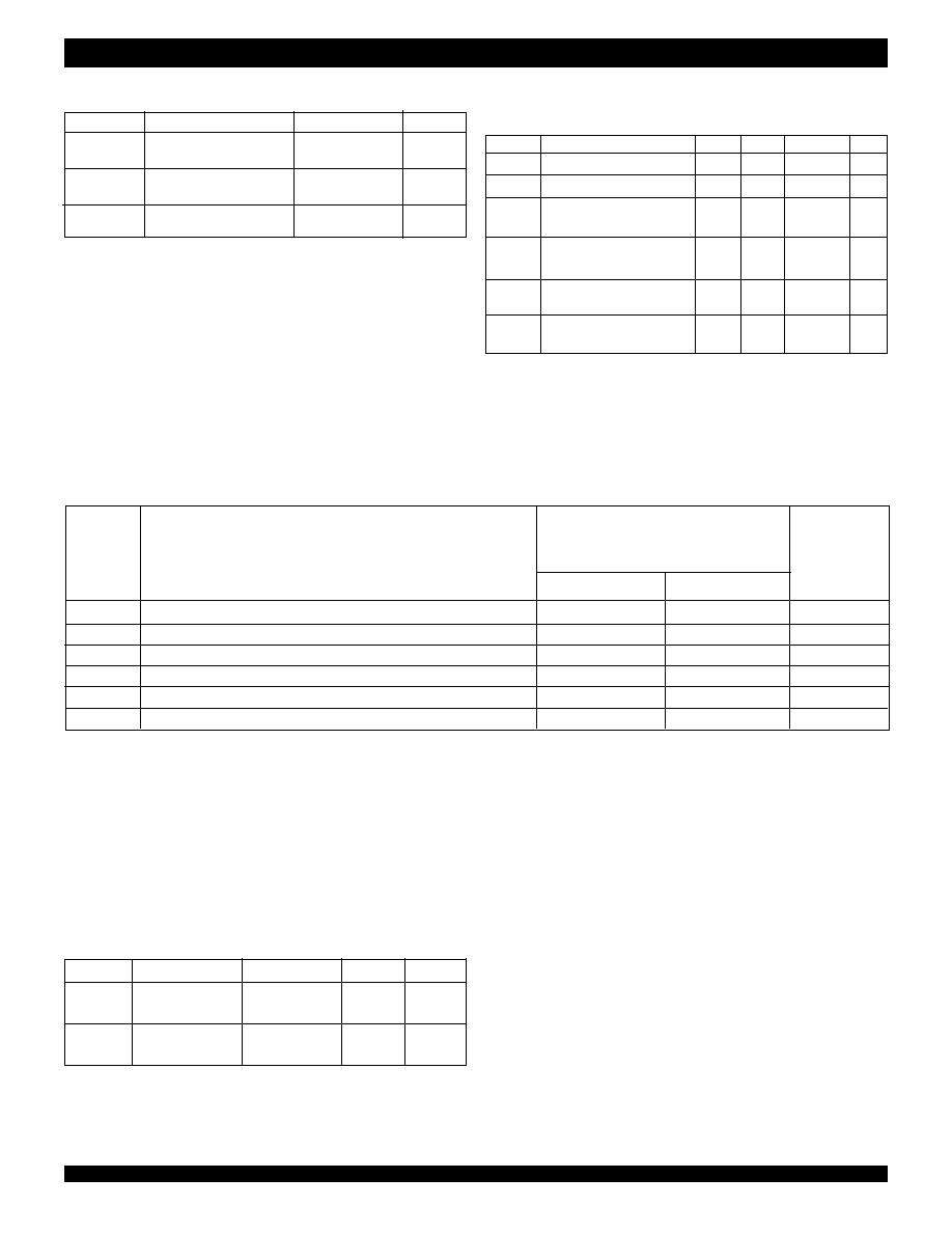
IDT72V275/72V285
Symbol
Rating
Commercial
Unit
V
TERM
Terminal Voltage
0.5 to +4.6
V
with respect to GND
T
STG
Storage
55 to +125
° C
Temperature
I
OUT
DC Output Current
50 to +50
mA
NOTES:
1. With output deselected, (
OE
V
IH
).
2. Characterized values, not currently tested.
DC ELECTRICAL CHARACTERISTICS
(Commercial: V
CC
= 3.3V ± 0.3V, T
A
= 0
o
C to +70
o
C; Industrial: V
CC =
3.3V
±
0.3V, TA = -40
°
C to +85
°
C)
Symbol
Parameter
(1)
Conditions
Max.
Unit
C
IN
(2)
Input
V
IN
= 0V
10
pF
Capacitance
C
OUT
(1,2)
Output
V
OUT
= 0V
10
pF
Capacitance
Symbol
Parameter
Min.
Typ.
Max.
Unit
V
CC
Supply Voltage(Com'l & Ind'l)
3.0
3.3
3.6
V
GND
Supply Voltage(Com'l & Ind'l)
0
0
0
V
V
IH
Input High Voltage
(Com'l & Ind'l)
2.0
--
V
CC
+ 0.5
V
V
IL
(1)
Input Low Voltage
(Com'l & Ind'l)
--
--
0.8
V
T
A
Operating Temperature
0
--
70
o
C
Commercial
T
A
Operating Temperature
-40
85
°
C
Industrial
NOTE:
1. 1.5V undershoots are allowed for 10ns once per cycle.
IDT72V275L
IDT72V285L
Com''l & Ind'l
(1)
t
CLK
= 10, 15, 20 ns
Symbol
Parameter
Min.
Max.
Unit
I
LI
(2)
Input Leakage Current
1
1
µ A
I
LO
(3)
Output Leakage Current
10
10
µA
V
OH
Output Logic "1" Voltage, I
OH
= 2 mA
2.4
--
V
V
OL
Output Logic "0" Voltage, I
OL
= 8 mA
--
0.4
V
I
CC1
(4,5,6)
Active Power Supply Current
--
60
mA
I
CC2
(4,7)
Standby Current
--
20
mA
NOTES
:
1.
Industrial temperature range product for the 15ns is available as a standard device.
2. Measurements with 0.4
V
IN
V
CC
.
3.
OE
V
IH,
0.4
V
OUT
V
CC.
4. Tested with outputs open (I
OUT
= 0).
5. RCLK and WCLK toggle at 20 MHz and data inputs switch at 10 MHz.
6. Typical I
CC1
= 11 + 1.65*f
S
+ 0.02*C
L
*f
S
(in mA) with V
CC
= 3.3V, t
A
= 25
o
C, f
S
= WCLK frequency = RCLK frequency (in MHz, using TTL levels), data switching at f
S
/2, C
L
= capacitive load (in pF).
7. All Inputs = V
CC
- 0.2V or GND + 0.2V, except RCLK and WCLK, which toggle at 20 MHz.
ABSOLUTE MAXIMUM RATINGS
NOTE:
1. Stresses greater than those listed under ABSOLUTE MAXIMUM RATINGS may cause
permanent damage to the device. This is a stress rating only and functional operation
of the device at these or any other conditions above those indicated in the operational
sections of this specification is not implied. Exposure to absolute maximum rating
conditions for extended periods may affect reliability.
RECOMMENDED DC OPERATING
CONDITIONS
CAPACITANCE
(T
A
= +25
o
C, f = 1.0MHz)