
MK3771-17
MDS 3771-17 C
1
Revision 083104
Integrated Circuit Systems, Inc.
525 Race Street, San Jose, CA 95126
tel (408) 297-1201
www.icst.com
VCXO and HDTV Set-Top Clock Source
Description
The MK3771-17 is a low cost, low jitter,
high-perfomance VCXO and clock synthesizer
designed for set-top boxes and HDTV receivers. The
on-chip Voltage Controlled Crystal Oscillator accepts a
0 to 3.3 V input voltage to cause the output clocks to
vary by ±100 ppm. Using ICS's patented VCXO and
analog Phase-Locked Loop (PLL) techniques, the
device uses an inexpensive 13.5 MHz crystal input to
produce multiple output clocks including selectable
BCLK, a selectable audio clock, two communications
clocks, a 13.5 MHz clock, and three 27 MHz clocks. All
clocks are frequency locked to the 27 MHz output (and
to each other) with zero ppm error, so any output can
be used as the VCXO output.
Features
·
Packaged in 28-pin SSOP
·
Available in Pb (lead) free package
·
HDTV frequencies of 74.25 and 74.175824 MHz
·
On-chip patented VCXO with pull range of 200 ppm
(minimum)
·
VCXO tuning voltage of 0 to 3.3 V
·
Supports Ethernet with 20 and 25 MHz clocks
·
Modem clocks of 11.0592 and 24.576 MHz option
·
Audio clocks support 32 kHz, 44.1 kHz, 48 kHz and
96 kHz sampling rates
·
Zero ppm synthesis error in all clocks (all exactly
track 27MHz VCXO)
·
Uses an inexpensive 13.5 MHz crystal
·
Full CMOS output swings with 12 mA output
·
drive capability at TTL levels
·
Advanced, low power, sub-micron CMOS process
·
3.3 V ±5% operating supply
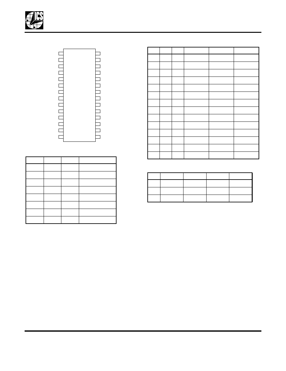
Block Diagram
Voltage
Controlled
Crystal
Oscillator
Divide
Logic
PLL Clock
Synthesis
Circuitry
AS2:0
BS1, BS0
CS
VIN
3
Audio Clock
BCLK
13.5 MHz
pullable crystal
XI
XO
2
CCLK1
CCLK2
108 MHz or 27 MHz
54 MHz or 27 MHz
27 MHz
13.5 MHz or 27 MHz
X8
PLL
VS
VCXO and HDTV Set-Top Clock Source
MDS 3771-17 C
2
Revision 083104
Integrated Circuit Systems, Inc.
525 Race Street, San Jose, CA 95126
tel (408) 297-1201
www.icst.com
MK3771-17
Pin Assignment
Audio Clocks (MHz)
B and C Clocks (MHz)
VCXO Clocks (MHz)
AS2
AS1
AS0
ACLK
0
0
0
8.192
0
0
1
11.2896
0
1
0
12.288
0
1
1
16.9344
1
0
0
16.384
1
0
1
22.5792
1
1
0
18.432
1
1
1
24.576
18
7
17
8
16
9
15
VDD
10
VDD
11
CS
12
AS2
13
GND
14
GND
GND
GND
VCLK3
BCLK
CCLK1
CCLK2
VS
BS1
22
21
20
19
ACLK
VDD
5
6
VDD
VIN
VCLK4
24
23
GND
3
4
X1
VDD
VCLK1
26
25
VCLK2
1
2
BS0
X2
AS0
28
27
AS1
BS1
BS0
CS
BCLK
CCLK1
CCLK2
0
0
0
74.175
20
25
0
0
1
74.175
11.0592
24.576
0
1
0
74.25
20
25
0
1
1
74.25
11.0592
24.576
M
0
0
5.06
20
25
M
0
1
5.06
11.0592
24.576
M
1
0
10.12
20
25
M
1
1
10.12
11.0592
24.576
1
0
0
48
20
25
1
0
M
48
7.3728
24
1
0
1
48
11.0592
24.576
1
1
0
14.318
20
25
1
1
M
14.318
7.3728
28.636
1
1
1
14.318
11.0592
24.576
VS
VCLK1
VCLK2
VCLK3
VCLK4
0
27
27
27
108
M
27
54
13.5
108
1
27
27
27
27

VCXO and HDTV Set-Top Clock Source
MDS 3771-17 C
3
Revision 083104
Integrated Circuit Systems, Inc.
525 Race Street, San Jose, CA 95126
tel (408) 297-1201
www.icst.com
MK3771-17
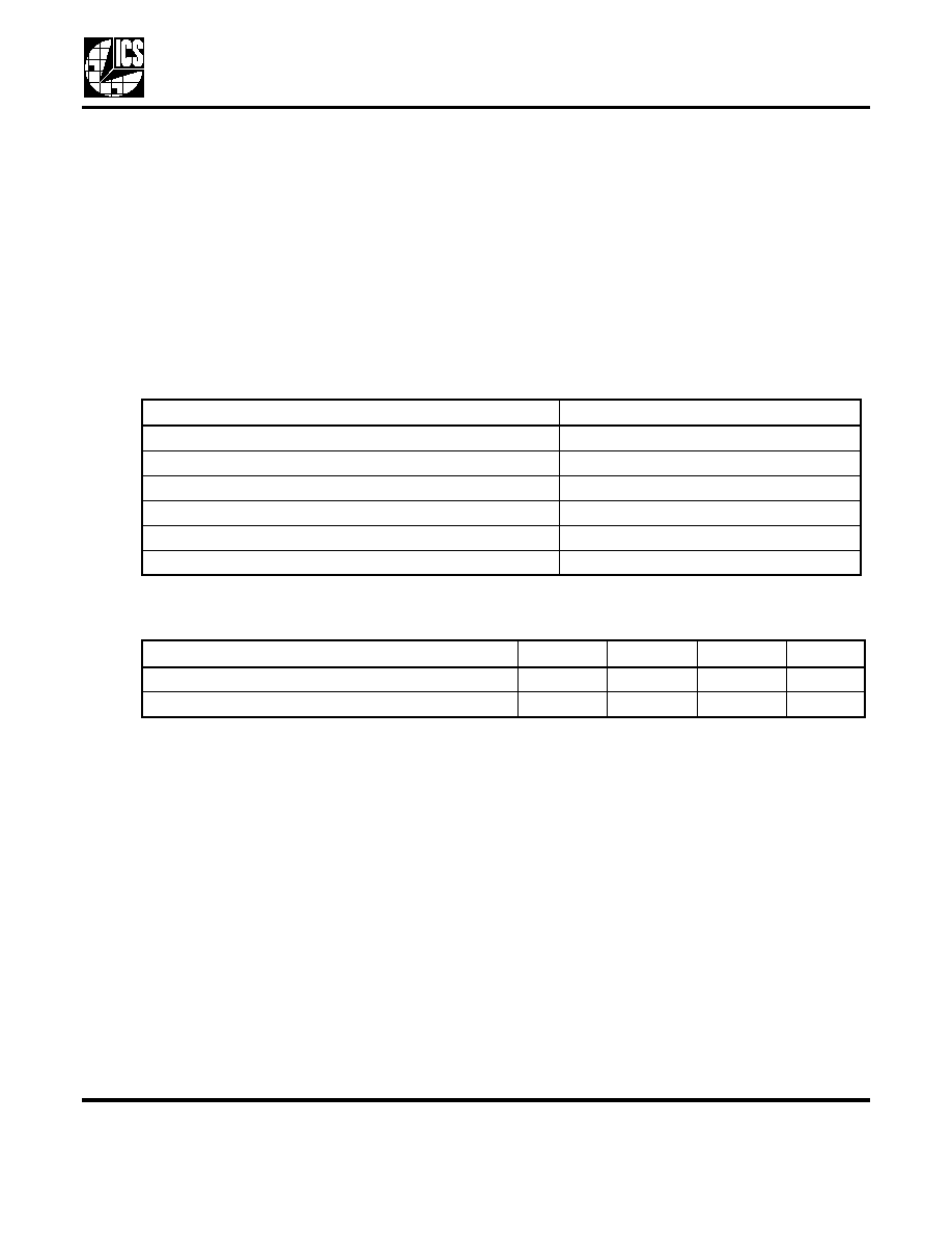
Pin Descriptions
KEY:
I = Input
TI = Tri-level
O = Output
P = Power supply connection
XI, XO= Crystal connections
Pin
Number
Pin
Name
Pin
Type
Pin Description
1
BS0
I
B clock select 0.
2
X2
XO
Crystal connection. Connect to a pullable 13.5 MHz crystal.
3
X1
XI
Crystal connection. Connect to a pullable 13.5 MHz crystal.
4, 5, 7, 8, 22
VDD
P
Connect to +3.3 V.
6
VIN
I
Analog control voltage for VCXO. Pulls outputs ±100 ppm by varying from
0 to 3.3 V.
9
CS
TI
Communications Clock Select. Selects CCLK 1 and 2 per table above.
Internal pull-up.
10, 11, 19,
20, 24
GND
P
Connect to ground.
12
BCLK
O
B clock output. Determined by status of AS2:0 per table above.
13
VS
TI
VCXO Clock Select. Selects frequencies on VCLK1-VCLK4 per table
above.
14
ACLK
O
Audio Clock Output. Determined by status of AS2:0 per table above.
15
CCLK2
O
Communications Clock Output 2. Determined by status of CS per table
above.
16
BS1
TI
B Clock Select 1. Selects BCLK frequency. See table above.
17
CCLK1
O
Communications Clock Output 1. Determined by status of CS per table
above.
18
VCLK3
O
VCXO Clock output 3. Can be either 27 or 13.5 MHz per table above.
21
AS2
I
Audio Clock Select pin 2. Selects Audio clock on pin 14 per table above.
Internal pull-up.
23
VCLK4
O
VCXO Clock output 4. Can be either 27 or 108 MHz per table above.
25
VCLK1
O
VCXO Clock output 1. Always 27 MHz.
26
VCLK2
O
VCXO Clock output 2. Can be either 27 or 54 MHz per table above.
27
AS0
I
Audio Clock Select pin 0. Selects Audio clock on pin 14 per table above.
Internal pull-up.
28
AS1
I
Audio Clock Select pin 1. Selects Audio clock on pin 14 per table above.
Internal pull-up.

VCXO and HDTV Set-Top Clock Source
MDS 3771-17 C
4
Revision 083104
Integrated Circuit Systems, Inc.
525 Race Street, San Jose, CA 95126
tel (408) 297-1201
www.icst.com
MK3771-17
External Component Selection
The MK3771-17 requires a minimum number of
external components for proper operation.
Decoupling Capacitors
Decoupling capacitors of 0.01
µF should be connected
between VDD and GND on pins 3 and 6, and on pins
13 and 14, as close to the MK3771-17 as possible. For
optimum device performance, the decoupling
capacitors should be mounted on the component side
of the PCB. Avoid the use of vias in the decoupling
circuit.
Series Termination Resistor
When the PCB traces between the clock outputs and
the loads are over 1 inch, series termination should be
used. To series terminate a 50
trace (a commonly
used trace impedance) place a 33
resistor in series
with the clock line, as close to the clock output pin as
possible. The nominal impedance of the clock output is
20
.
Quartz Crystal
The MK3771-17 VCXO function consists of the
external crystal and the integrated VCXO oscillator
circuit. To assure the best system performance
(frequency pull range) and reliability, a crystal device
with the recommended parameters must be used, and
the layout guidelines discussed in the following section
must be followed.
The frequency of oscillation of a quartz crystal is
determined by its "cut" and by the load capacitors
connected to it. The MK3771-17 incorporates on-chip
variable load capacitors that "pull" (change) the
frequency of the crystal. The crystal specified for use
with the MK3771-17 is designed to have zero
frequency error when the total of on-chip + stray
capacitance is 14 pF.
The external crystal must be connected as close to the
chip as possible and should be on the same side of the
PCB as the MK3771-17. There should be no vias
between the crystal pins and the X1 and X2 device
pins. There should be no signal traces underneath or
close to the crystal.
Please see application note MAN05 for recommended
crystal parameters and suppliers.
Crystal Tuning Load Capacitors
The crystal traces should include pads for small fixed
capacitors, one between X1 and ground, and another
between X2 and ground. Stuffing of these capacitors
on the PCB is optional. The need for these capacitors is
determined at system prototype evaluation, and is
influenced by the particular crystal used (manufacture
and frequency) and by PCB layout. The typical required
capacitor value is 1 to 4 pF.
To determine the need for and value of the crystal
adjustment capacitors, you will need a PC board of
your final layout, a frequency counter capable of about
1 ppm resolution and accuracy, two power supplies,
and some samples of the crystals which you plan to
use in production, along with measured initial accuracy
for each crystal at the specified crystal load
capacitance, CL.
To determine the value of the crystal capacitors:
1. Connect VDD of the MK3771-17 to 3.3 V. Connect
pin 4 of the MK3771-17 to the second power supply.
Adjust the voltage on pin 4 to 0V. Measure and record
the frequency of the CLK output.
2. Adjust the voltage on pin 4 to 3.3 V. Measure and
record the frequency of the same output.
To calculate the centering error:
Where:
f
target
= nominal crystal frequency
error
xtal
=actual initial accuracy (in ppm) of the crystal
being measured
If the centering error is less than ±25 ppm, no
adjustment is needed. If the centering error is more
than 25ppm negative, the PC board has excessive
stray capacitance and a new PCB layout should be
considered to reduce stray capacitance. (Alternately,
the crystal may be re-specified to a higher load
capacitance. Contact ICS for details.) If the centering
error is more than 25ppm positive, add identical fixed
centering capacitors from each crystal pin to ground.
The value for each of these caps (in pF) is given by:
External Capacitor =
2 x (centering error)/(trim sensitivity)
Error
10
6
x
f
3.3V
f
t
et
arg
(
)
f
0V
f
t
et
arg
(
)
+
f
t
et
arg
------------------------------------------------------------------------------
error
xtal
=
VCXO and HDTV Set-Top Clock Source
MDS 3771-17 C
5
Revision 083104
Integrated Circuit Systems, Inc.
525 Race Street, San Jose, CA 95126
tel (408) 297-1201
www.icst.com
MK3771-17
Trim sensitivity is a parameter which can be supplied by
your crystal vendor. If you do not know the value,
assume it is 30 ppm/pF. After any changes, repeat the
measurement to verify that the remaining error is
acceptably low (typically less than ±25ppm).
Absolute Maximum Ratings
Stresses above the ratings listed below can cause permanent damage to the MK3771-17. These ratings,
which are standard values for ICS commercially rated parts, are stress ratings only. Functional operation of
the device at these or any other conditions above those indicated in the operational sections of the
specifications is not implied. Exposure to absolute maximum rating conditions for extended periods can
affect product reliability. Electrical parameters are guaranteed only over the recommended operating
temperature range.
Recommended Operation Conditions
Item
Rating
Supply Voltage, VDD
7 V
All Inputs and Outputs
-0.5 V to VDD+0.5 V
Ambient Operating Temperature
0 to +70
°C
Storage Temperature
-65 to +150
°C
Junction Temperature
125
°C
Soldering Temperature
260
°C
Parameter
Min.
Typ.
Max.
Units
Ambient Operating Temperature
0
+70
°C
Power Supply Voltage (measured in respect to GND)
+3.15
+3.3
+3.45
V