Äîêóìåíòàöèÿ è îïèñàíèÿ www.docs.chipfind.ru
MK2049-45
MDS 2049-45 G
1
Revision 101904
Integrated Circuit Systems, Inc.
525 Race Street, San Jose, CA 95126
tel (408) 297-1201
www.icst.com
3.3V Communications Clock PLL
Description
The MK2049-45 is a dual Phase-Locked Loop (PLL)
device which can provide frequency synthesis and jitter
attenuation. The first PLL is VCXO based and uses a
pullable crystal to track signal wander and attenuate
input jitter. The second PLL is a translator for frequency
multiplication. Basic configuration is determined by a
Mode/Frequency Selection Table. Loop bandwidth and
damping factor are programmable via external loop
filter component selection.
Buffer Mode accepts a 10 to 50MHz input and will
provide a jitter attenuated output at 0.5 x ICLK, 1 x
ICLK or 2 x ICLK. In this mode the MK2049-45 is ideal
for filtering jitter from high frequency clocks.
In External Mode, ICLK accepts an 8 kHz clock and will
produce output frequencies from a table of common
communciations clock rates, CLK and CLK/2. This
allows for the generation of clocks frequency-locked to
an 8 kHz backplane clock, simplifying clock
synchronization in communications systems.
The MK2049-45 can be dynamically switched between
T1, E1, T3, E3 outputs with the same 24.576 MHz
crystal.
ICS can customize these devices for many other
different frequencies. Contact your ICS representative
for more details.
Features
·
Packaged in 20 pin SOIC
·
3.3 V + 5% operation
·
Meets the TR62411, ETS300 011, and GR-1244
specification for MTIE, Pull-in/Hold-in Range, Phase
Transients, and Jitter Generation for Stratum 3, 4,
and 4E
·
Accepts multiple inputs: 8 kHz backplane clock, or 10
to 50 MHz
·
Locks to 8 kHz + 100 ppm (External mode)
·
Buffer Mode allows jitter attenuation of 10 - 50 MHz
input and x1 / x0.5 or x1 / x2 outputs
·
Exact internal ratios enable zero ppm error
·
Output rates include T1, E1, T3, E3, and OC3
submultiples
·
Available in Pb (lead) free package
·
See also the MK2049-34 and MK2049-36
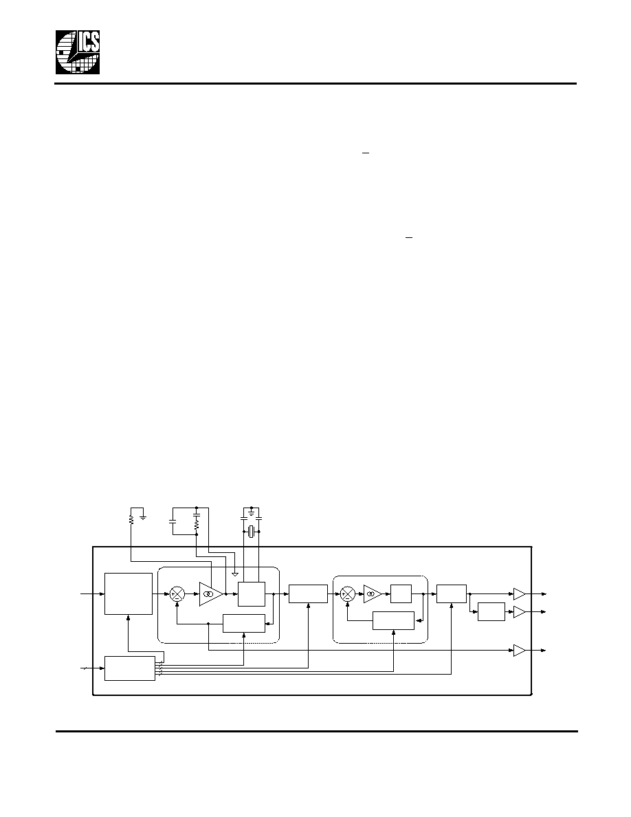
Block Diagram
Charge
Pump
VCXO
X2
X1
ISET
CAP2
Feedback
Divider (N)
Reference
Divider
(used in buffer
mode only)
ICLK
Reference
Divider
Phase
Detector
VCXO
PLL
Feedback
Divider
VCO
Translator
PLL
CLK
CAP1
Output
Divider
Divide
by 2
CLK/2
8k
R
S
R
SET
C
P
C
S
Optional Crystal Load Caps
Divider Value
Look-up Table
FS3:0
4
C
L
C
L
External Pullable Crystal
3.3V Communications Clock PLL
MDS 2049-45 G
2
Revision 101904
Integrated Circuit Systems, Inc.
525 Race Street, San Jose, CA 95126
tel (408) 297-1201
www.icst.com
MK2049-45
Pin Assignment
Pin Descriptions
16
1
15
2
14
FS1
FS0
3
13
X2
4
12
X1
RES
5
11
VDD
6
CAP2
7
FCAP
8
VDD
GND
CAP1
VDD
GND
GND
CLK
ICLK
9
10
CLK/2
FS3
8k
FS2
20
19
18
17
Pin
Number
Pin
Name
Pin
Type
Pin Description
1
FS1
Input
Frequency select 1. Determines CLK input/outputs per table on page 2.
Internal pull-up resistor.
2
X2
Input
Crystal connection. Connect to a MHz crystal as shown in table on page 2.
3
X1
Input
Crystal connection. Connect to a MHz crystal as shown in table on page 2.
4
VDD
Power
Power supply. Connect to +3.3V.
5
FCAP
-
Filter capacitor. Connect a 1000 pF ceramic capacitor to ground.
6
VDD
Power
Power supply. Connect to +3.3V.
7
GND
Power
Connect to ground
8
CLK
Output
Clock output determined by status of FS3:0 per tables on page 2.
9
CLK/2
Output
Clock output determined by status of FS3:0 per tables page 2. Always 1/2 of
CLK.
10
8k
Output
Recovered 8 kHz clock output.
11
FS2
Input
Frequency select 2. Determines CLK input/outputs per table on page 2.
Internal pull-up resistor.
12
FS3
Input
Frequency select 3. Determines CLK input/outputs per table on page 2.
Internal pull-up resistor.
13
ICLK
Input
Input clock connection. Connect to 8 kHz backplane or MHz clock.
14
GND
Power
Connect to ground.
15
VDD
Power
Power Supply. Connect to +3.3V.
16
CAP1
Loop
Filter
Connect the loop filter capacitors and resistor between this pin and CAP2.
17
GND
Power
Connect to ground.
3.3V Communications Clock PLL
MDS 2049-45 G
3
Revision 101904
Integrated Circuit Systems, Inc.
525 Race Street, San Jose, CA 95126
tel (408) 297-1201
www.icst.com
MK2049-45
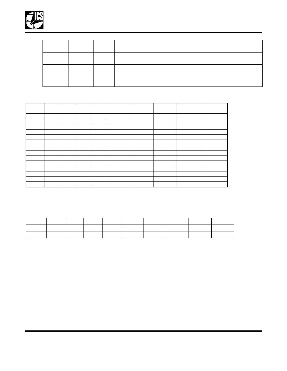
Output Decoding Table - External Mode (MHz)
Output Decoding Table - Buffer Mode (MHz)
0 = connect directly to ground, 1 = connect directly to VDD
Crystal is connected to pins 2 and 3; clock input is applied to pin 13.
Functional Description
The MK2049-45 is a clock generator IC that generates
an output clock directly from an internal VCXO circuit
which works in conjunction with an external quartz
crystal. The VCXO is controlled by an internal PLL
(Phase Locked Loop) circuit, enabling the device to
perform clock regeneration from an input reference
clock. The MK2049-45 is configured to provide a high
frequency communications reference clock output from
an 8 kHz input clock or to jitter attenuate and buffer a
high frequency input clock. There are 14 selectable
output frequencies and two buffer mode selections.
Please refer to the Output Clock Selection Table on
Page 2.
Most typical PLL clock devices use an internal VCO
(Voltage Controlled Oscillator) for output clock
generation. By using a VCXO with an external crystal,
18
CAP2
Loop
Filter
Connect the loop filter capacitors and resistor between this pin and CAP1.
19
RES
-
Connect a resistor to ground. See table.
20
FS0
Input
Frequency select 0. Determines CLK input/outputs per table on page 2.
Internal pull-up resistor.
ICLK
FS3
FS2
FS1
FS0
CLK/2
CLK
8k
Crystal
Used (MHz)
N
8 kHz
0
0
0
0
1.544
3.088
8 kHz
24.576
3072
8 kHz
0
0
0
1
2.048
4.096
8 kHz
24.576
3072
8 kHz
0
0
1
0
22.368
44.736
8 kHz
24.576
3072
8 kHz
0
0
1
1
17.184
34.368
8 kHz
24.576
3072
8 kHz
0
1
0
0
19.44
38.88
8 kHz
19.44
2430
8 kHz
0
1
0
1
12.8
25.6
8 kHz
25.6
3200
8 kHz
0
1
1
0
25.92
51.84
8 kHz
17.28
2160
8 kHz
0
1
1
1
4.096
8.192
8 kHz
16.384
2048
8 kHz
1
0
0
0
18.528
37.056
8 kHz
24.704
3088
8 kHz
1
0
0
1
12.352
24.704
8 kHz
24.704
3088
8 kHz
1
0
1
0
24.576
49.152
8 kHz
16.384
2048
8 kHz
1
0
1
1
16.384
32.768
8 kHz
16.384
2048
8 kHz
1
1
0
0
17.28
34.56
8 kHz
17.28
2160
8 kHz
1
1
0
1
62.5
125
8 kHz
25
3125
Pin
Number
Pin
Name
Pin
Type
Pin Description
ICLK
FS3
FS2
FS1
FS0
CLK/2
CLK
8k
Crystal
N
20 - 50
1
1
1
0
ICLK
2*ICLK
N/A
ICLK/2
3
10 - 25
1
1
1
1
ICLK/2
ICLK
N/A
ICLK
3
3.3V Communications Clock PLL
MDS 2049-45 G
4
Revision 101904
Integrated Circuit Systems, Inc.
525 Race Street, San Jose, CA 95126
tel (408) 297-1201
www.icst.com
MK2049-45
the MK2049-45 is able to generate a low jitter, low
phase-noise output clock within a low bandwidth PLL.
This serves to provide input clock jitter attenuation and
enables stable operation with a low frequency
reference clock.
The VCXO circuit requires an external pullable crystal
for operation. External loop filter components enable a
PLL configuration with low loop bandwidth.
Application Information
Output Frequency Configuration
The MK2049-45 is configured to generate a set of
output frequencies from an 8 kHz input clock. Please
refer to the Output Clock Selection Table on Page 2.
Input bits FS3:0 are set according to this table, as is the
external crystal frequency. Please refer to the Quartz
Crystal section on this page regarding external crystal
requirements.
Quartz Crystal
It is important that the correct type of quartz crystal is
used with the MK2049-45. Failure to do so may result in
reduced frequency pullability range, inability of the loop
to lock, or excessive output phase jitter.
The MK2049-45 operates by phase-locking the VCXO
circuit to the input signal of the selected ICLK input.
The VCXO consists of the external crystal and the
integrated VCXO oscillator circuit. To achieve the best
performance and reliability, a crystal device with the
recommended parameters (shown below) must be
used, and the layout guidelines discussed in the PCB
Layout Recommendations section must be followed.
The frequency of oscillation of a quartz crystal is
determined by its cut and by the external load
capacitance. The MK2049-45 incorporates variable
load capacitors on-chip which "pull", or change, the
frequency of the crystal. The crystals specified for use
with the MK2049-45 are designed to have zero
frequency error when the total of on-chip + stray
capacitance is 14 pF. To achieve this, the layout should
use short traces between the MK2049-45 and the
crystal.
A complete description of the recommended crystal
parameters in the ICS application note, MAN05.
To obtain a list of qualified crystal devices please visit
our website at:
http://www.icst.com/products/telecom/vcxocrystals.htm
PLL Loop Filter Components
All analog PLL circuits use a loop filter to establish
operating stability. The MK2049-45 uses external loop
filter components for the following reasons:
1) Larger loop filter capacitor values can be used,
allowing a lower loop bandwidth. This enables the use
of lower input clock reference frequencies and also
input clock jitter attenuation capabilities. Larger loop
filter capacitors also allow higher loop damping factors
when less passband peaking is desired.
2) The loop filter values can be user selected to
optimize loop response characteristics for a given
application.
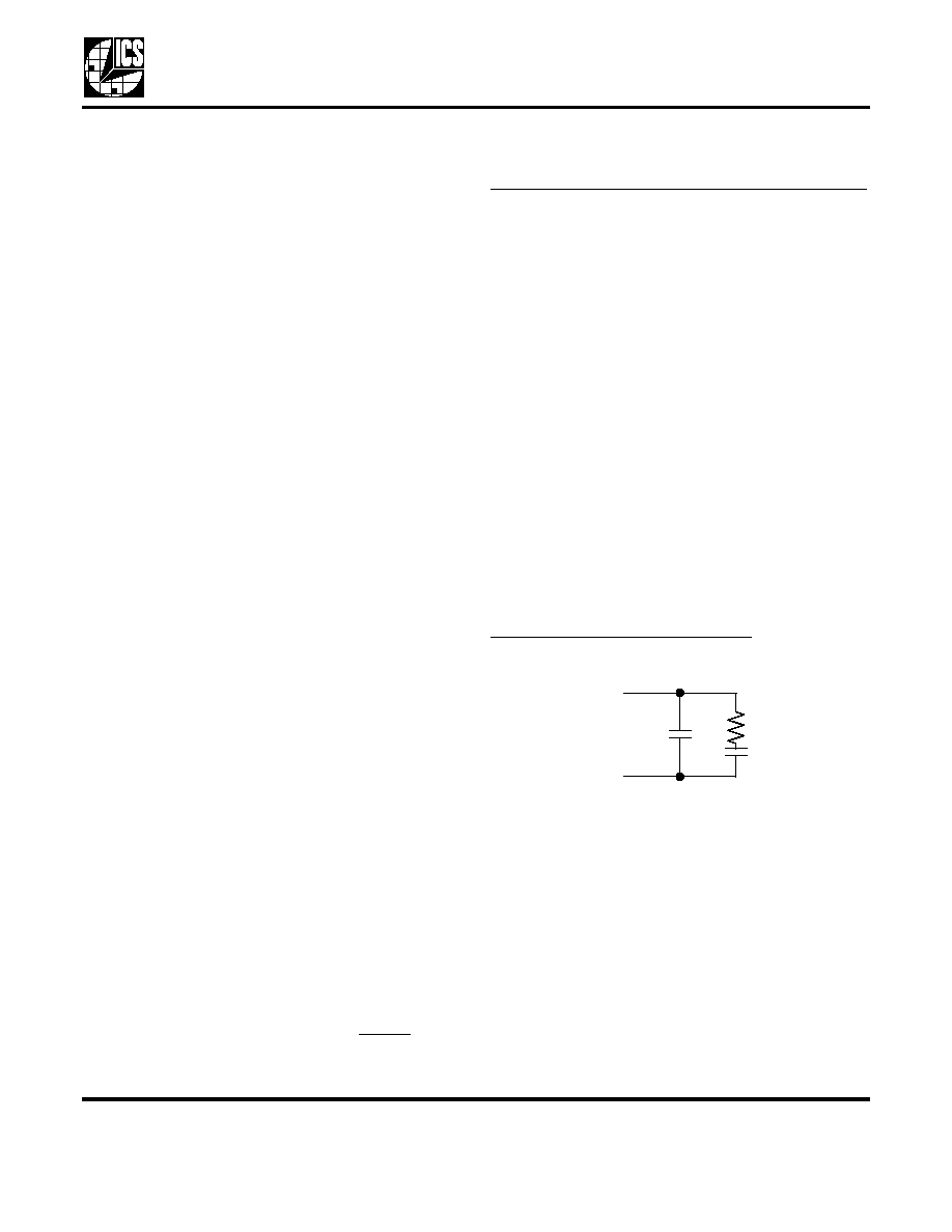
Referencing the External Component Schematic on
this page, the external loop filter is made up of
components R
S
, C
S
and C
P
. R
SET
establishes PLL
charge pump current and therefore influences loop
filter characteristics.
Tools for optimizing the values of these four
components can be found at:
http://www.icst.com/products/telecom/
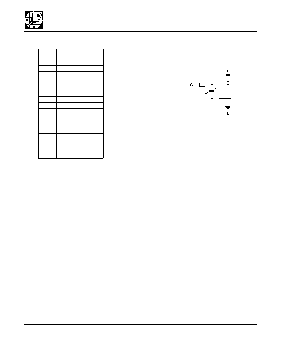
CAP2
CAP1
0.0003 µF
820 kohms
0.1 µF
Figure 3. Typical Loop Filter
R
S
C
P
C
S
3.3V Communications Clock PLL
MDS 2049-45 G
5
Revision 101904
Integrated Circuit Systems, Inc.
525 Race Street, San Jose, CA 95126
tel (408) 297-1201
www.icst.com
MK2049-45
Charge Pump Current Table
Special considerations must be made in choosing loop
components C
S
and C
P
. These recommendations can
be found at
http://www.icst.com/products/telecom/loopfiltercap.htm
Series Termination Resistor
Clock output traces over one inch should use series
termination. To series terminate a 50
trace (a
commonly used trace impedance), place a 33
resistor
in series with the clock line, as close to the clock output
pin as possible. The nominal impedance of the clock
output is 20
. (The optional series termination resistor
is not shown in the External Component Schematic.)
Decoupling Capacitors
As with any high performance mixed-signal IC, the
MK2049-45 must be isolated from system power
supply noise to perform optimally.
Decoupling capacitors of 0.01µF must be connected
between each VDD and the PCB ground plane. To
further guard against interfering system supply noise,
the MK2049-45 should use one common connection to
the PCB power plane as shown in the diagram on the
next page. The ferrite bead and bulk capacitor help
reduce lower frequency noise in the supply that can
lead to output clock phase modulation.
Recommended Power Supply Connection
for Optimal Device Performance
Crystal Load Capacitors
The device crystal connections should include pads for
small capacitors from X1 to ground and from X2 to
ground, shown as C
L
in the External Component
Schematic. These capacitors are used to adjust the
stray capacitance of the board to match the nominally
required crystal load capacitance. Because load
capacitance can only be increased in this trimming
process, it is important to keep stray capacitance to a
minimum by using very short PCB traces (and no vias)
been the crystal and device.
Please refer to MAN05 for the procedure to determine
capacitor values.
PCB Layout Recommendations
For optimum device performance and lowest output
phase noise, the following guidelines should be
observed. Please also refer to the Recommended PCB
Layout drawing on Page 7.
1) Each 0.01 µF decoupling capacitor should be
mounted on the component side of the board as close
to the VDD pin as possible. No via's should be used
between decoupling capacitor and VDD pin. The PCB
trace to VDD pin should be kept as short as possible,
as should the PCB trace to the ground via. Distance of
the ferrite bead and bulk decoupling from the device is
less critical.
2) The loop filter components must also be placed
close to the CHGP and VIN pins. C
P
should be closest
to the device. Coupling of noise from other system
R
SET
(k
)
Charge Pump Current
(I
CP
) (
µA)
13.02
139
15
125
16
119
18
109
20
100
22
93
24
86
27
68
36
56
47
43
56
35
75
28
100
22
150
15
200
12
Connection to 3.3V
Power Plane
Ferrite
Bead
Bulk Decoupling Capacitor
(such as 1 µF Tantalum)
VDD Pin
VDD Pin
VDD Pin
0.01 µF Decoupling Capacitors
Document Outline