Integrated
Circuit
Systems, Inc.
ICS9248- 143
Block Diagram
Pentium is a trademark of Intel Corporation
I
2
C is a trademark of Philips Corporation
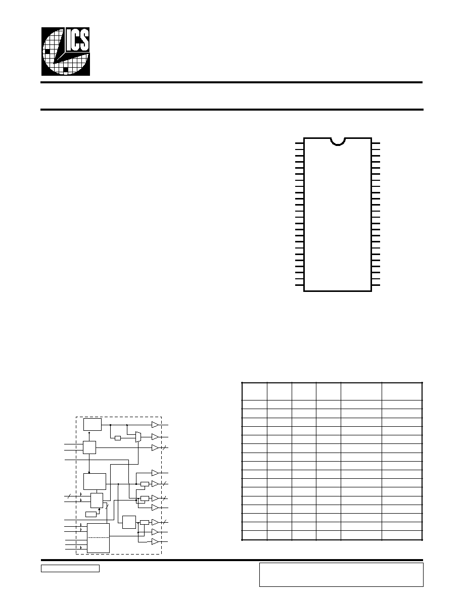
Frequency Generator & Integrated Buffers for PENTIUM
II
/
III
TM
& K6
9248-143 Rev C 7/26/00
Pin Configuration
48-Pin SSOP and TSSOP
* Internal Pull-up Resistor of 120K to VDD
CLK_STOP#
PCI_STOP#
CPU2.5_3.3#
PLL2
PLL1
Spread
Spectrum
48MHz
24_48MHz
CPUCLK_F
CPUCLK [2:0]
SDRAM [7:0]
PCICLK [5:0]
PCICLK_F
PCICLK_E
SDRAM_F
X1
X2
BUFFER IN
XTAL
OSC
PCI
CLOCK
DIVDER
STOP
STOP
STOP
SDATA
SCLK
PD#
FS(0:3)
SEL24_48#
Control
Logic
Config.
Reg.
/ 2
REF[1:0]
LATCH
POR
2
3
8
6
4
4
VDDREF
*SPREAD/REF0
GNDREF
X1
X2
VDDPCI
*CPU2.5_3.3#/PCICLK_F
*FS3/PCICLK0
GNDPCI
*SEL24_48#/PCICLK1
*SELPCIE_6#/PCICLK2
PCICLK3
PCICLK4
VDDPCI
BUFFER IN
GNDPCI
PCICLK5
PCICLK6/
VDDCOR
PCI_STOP#
*PD#
GND48
SDATA
SCLK
PCICLK_E
REF1/FS2*
VDDLCPU
CPUCLK_F
CPUCLK0
GNDLCPU
CPUCLK1
CPUCLK2
CLK_STOP#
GNDSDR
SDRAM_F
SDRAM0
SDRAM1
VDDSDR
SDRAM2
SDRAM3
GNDSDR
SDRAM4
SDRAM5
VDDSDR
SDRAM6
SDRAM7
VDD48
48MHz/FS0*
24_48MHz/FS1*
ICS9248-143
1
2
3
4
5
6
7
8
9
10
11
12
13
14
15
16
17
18
19
20
21
22
23
24
48
47
46
45
44
43
42
41
40
39
38
37
36
35
34
33
32
31
30
29
28
27
26
25
Recommended Application:
440BX, MX, VIA Apollo Pro 133, Apollo Pro Media
or MVP4 style chip set, for Note book applications.
Output Features:
4 - CPUs @ 2.5V/3.3V
including 1 free running CPUCLK_F
9 - SDRAM @ 3.3V
7 - PCI @ 3.3V, including 1 free running PCICLK_F
1 - PCI Early @ 3.3V
1 - 48MHz, @ 3.3V fixed.
1 - 24/48MHz @ 3.3V
2 - REF @3.3V, 14.318MHz.
Features:
Up to 137MHz frequency support
97MHz to support high-end AMD processor.
Support power management: CLK, PCI, stop and Power
down Mode from I
2
C programming.
Spread spectrum for EMI control
(±.25% & 0 to -0.5% down spread).
Uses external 14.318MHz crystal
FS pins for frequency select
Key Specifications:
CPU Output Jitter @ 2.5V: <300ps
CPU Output Jitter @ 3.3V: <250ps
PCI Output Jitter @ 3.3V: <250ps
CPU Output Skew @ 2.5V: <175ps
CPU Output Skew @ 3.3V: <175ps
PCI Output Skew @ 3.3V: <500ps
PCI Early to PCI Skew @ 3.3V: typ = 3ns
Functionality
3
S
F
2
S
F
1
S
F
0
S
F
U
P
C
)
z
H
M
(
I
C
P
)
z
H
M
(
0
0
0
0
7
6
.
6
6
3
3
.
3
3
0
0
0
1
0
0
.
0
0
1
3
3
.
3
3
0
0
1
0
0
3
.
0
0
1
3
4
.
3
3
0
0
1
1
3
3
.
3
3
1
3
3
.
3
3
0
1
0
0
0
0
.
5
0
1
0
0
.
5
3
0
1
0
1
7
3
.
3
3
1
4
3
.
3
3
0
1
1
0
0
0
.
7
3
1
5
2
.
4
3
0
1
1
1
0
0
.
5
7
0
5
.
7
3
1
0
0
0
0
0
.
0
0
1
3
3
.
3
3
1
0
0
1
0
0
.
5
9
7
6
.
1
3
1
0
1
0
0
0
.
7
9
3
3
.
2
3
1
0
1
1
3
3
.
3
3
1
3
3
.
3
3
1
1
0
0
0
0
.
0
9
0
0
.
0
3
1
1
0
1
2
2
.
6
9
7
0
.
2
3
1
1
1
0
2
8
.
6
6
1
4
.
3
3
1
1
1
1
0
5
.
1
9
0
5
.
0
3
ICS reserves the right to make changes in the device data identified in
this publication without further notice. ICS advises its customers to
obtain the latest version of all device data to verify that any
information being relied upon by the customer is current and accurate.
3
ICS9248-143
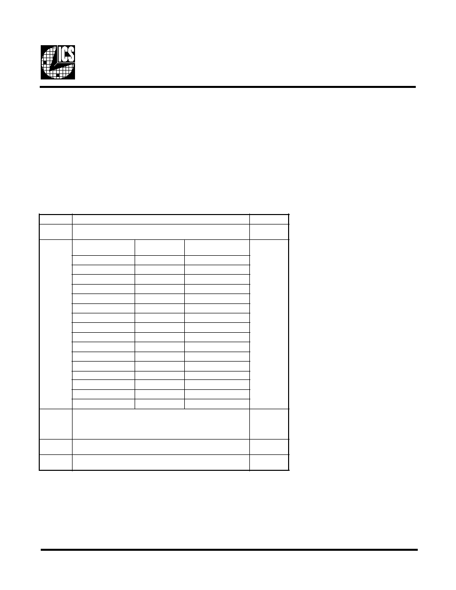
Byte0: Functionality and Frequency Select Register (default = 0)
Serial Configuration Command Bitmap
Notes:
1, Default at Power-up will be for latched logic inputs to define frequency. Bit [2, 6:4] are default to 0011.
2, PWD = Power-Up Default
The ICS9248-143 is the single chip clock solution for Notebook designs using thE 440BX, MX, VIA Apollo Pro 133, Apollo Pro
Media or MVP4 style chip set. It provides all necessary clock signals for such a system.
Spread spectrum may be enabled through I
2
C programming. Spread spectrum typically reduces system EMI by 8dB to 10dB.
This simplifies EMI qualification without resorting to board design iterations or costly shielding. The ICS9248-143 employs a
proprietary closed loop design, which tightly controls the percentage of spreading over process and temperature variations.
General Description
t
i
B
n
o
i
t
p
i
r
c
s
e
D
D
W
P
7
t
i
B
d
a
e
r
p
S
r
e
t
n
e
C
,
n
o
i
t
a
l
u
d
o
M
m
u
r
t
c
e
p
S
d
a
e
r
p
S
%
5
2
.
0
±
-
0
d
a
e
r
p
S
n
w
o
D
%
5
.
0
-
o
t
0
-
1
1
t
i
B
]
4
:
6
,
2
[
]
4
:
6
,
2
[
t
i
B
K
L
C
U
P
C
)
z
H
M
(
K
L
C
I
C
P
)
z
H
M
(
1
e
t
o
N
0
0
0
0
7
6
.
6
6
3
3
.
3
3
1
0
0
0
0
0
.
0
0
1
3
3
.
3
3
0
1
0
0
0
3
.
0
0
1
3
4
.
3
3
1
1
0
0
3
3
.
3
3
1
3
3
.
3
3
0
0
1
0
0
0
.
5
0
1
0
0
.
5
3
1
0
1
0
7
3
.
3
3
1
4
3
.
3
3
0
1
1
0
0
0
.
7
3
1
5
2
.
4
3
1
1
1
0
0
0
.
5
7
0
5
.
7
3
0
0
0
1
0
0
.
0
0
1
3
3
.
3
3
1
0
0
1
0
0
.
5
9
7
6
.
1
3
0
1
0
1
0
0
.
7
9
3
3
.
2
3
1
1
0
1
3
3
.
3
3
1
3
3
.
3
3
0
0
1
1
0
0
.
0
9
0
0
.
0
3
1
0
1
1
2
2
.
6
9
7
0
.
2
3
0
1
1
1
2
8
.
6
6
1
4
.
3
3
1
1
1
1
0
5
.
1
9
0
5
.
0
3
3
t
i
B
e
r
a
w
d
r
a
h
y
b
d
e
t
c
e
l
e
s
e
r
a
m
u
r
t
c
e
p
S
d
a
e
r
p
S
d
n
a
y
c
n
e
u
q
e
r
F
-
0
s
t
u
p
n
i
d
e
h
c
t
a
l
,
t
c
e
l
e
s
s
i
m
u
r
t
c
e
p
S
d
a
e
r
p
S
;
]
4
:
6
,
2
[
t
i
B
y
b
d
e
t
c
e
l
e
s
s
i
y
c
n
e
u
q
e
r
F
-
1
1
t
i
b
y
b
d
e
t
c
e
l
e
s
0
1
t
i
B
l
a
m
r
o
N
-
0
d
e
l
b
a
n
E
m
u
r
t
c
e
p
S
d
a
e
r
p
S
-
1
1
0
t
i
B
g
n
i
n
n
u
R
-
0
s
t
u
p
t
u
o
l
l
a
e
t
a
t
s
i
r
T
-
1
0
4
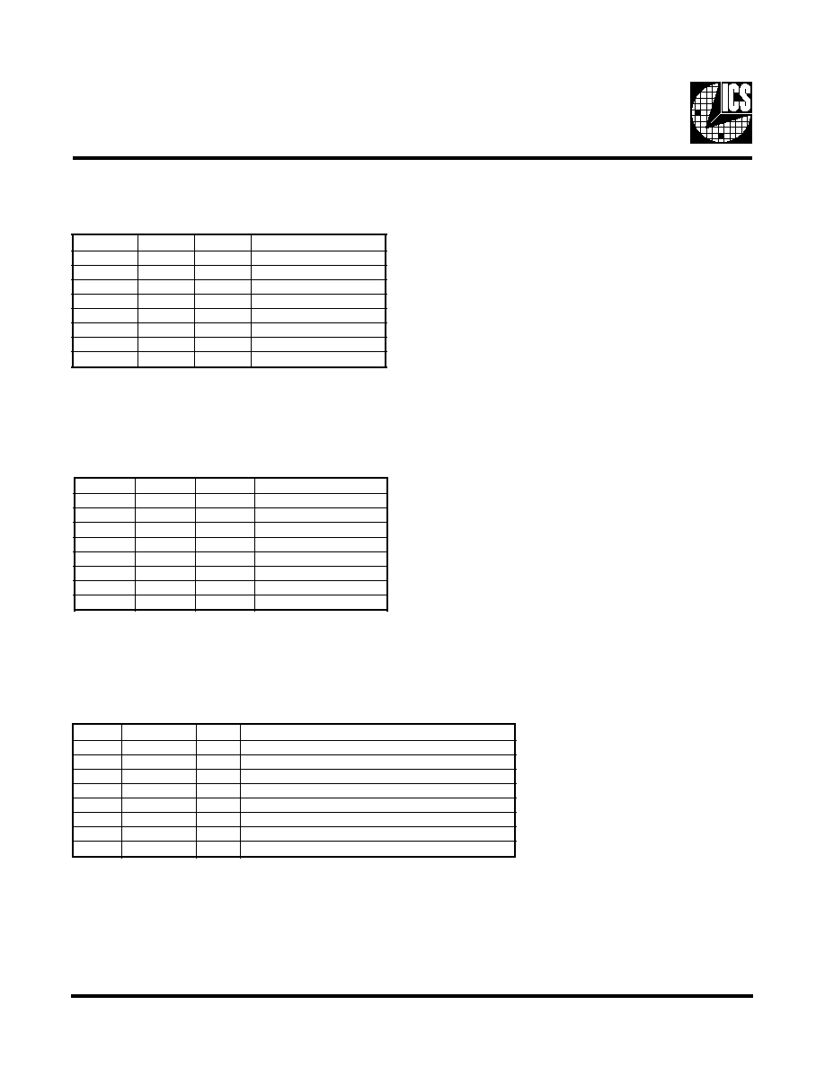
ICS9248-143
Notes:
1. Inactive means outputs are held LOW and are disabled from switching.
2. Latched Frequency Selects (FS#) will be inverted logic load of the input frequency select pin conditions.
Byte 2: PCI Active/Inactive Register (1 = enable, 0 = disable)
t
i
B
#
n
i
P
D
W
P
n
o
i
t
p
i
r
c
s
e
D
7
t
i
B
7
1
)
t
c
a
n
I
/
t
c
A
(
F
_
K
L
C
I
C
P
6
t
i
B
8
1
1
)
t
c
a
n
I
/
t
c
A
(
6
K
L
C
I
C
P
5
t
i
B
7
1
1
)
t
c
a
n
I
/
t
c
A
(
5
K
L
C
I
C
P
4
t
i
B
3
1
1
)
t
c
a
n
I
/
t
c
A
(
4
K
L
C
I
C
P
3
t
i
B
2
1
1
)
t
c
a
n
I
/
t
c
A
(
3
K
L
C
I
C
P
2
t
i
B
1
1
1
)
t
c
a
n
I
/
t
c
A
(
2
K
L
C
I
C
P
1
t
i
B
0
1
1
)
t
c
a
n
I
/
t
c
A
(
1
K
L
C
I
C
P
0
t
i
B
8
1
)
t
c
a
n
I
/
t
c
A
(
0
K
L
C
I
C
P
Byte 1: CPU, Active/Inactive Register (1 = enable, 0 = disable)
t
i
B
#
n
i
P
D
W
P
n
o
i
t
p
i
r
c
s
e
D
7
t
i
B
-
1
)
d
e
v
r
e
s
e
R
(
6
t
i
B
6
4
1
)
t
c
a
n
I
/
t
c
A
(
F
_
K
L
C
U
P
C
5
t
i
B
-
1
)
d
e
v
r
e
s
e
R
(
4
t
i
B
-
1
)
d
e
v
r
e
s
e
R
(
3
t
i
B
9
3
1
)
t
c
a
n
I
/
t
c
A
(
F
_
M
A
R
D
S
2
t
i
B
2
4
1
)
t
c
a
n
I
/
t
c
A
(
2
K
L
C
U
P
C
1
t
i
B
3
4
1
)
t
c
a
n
I
/
t
c
A
(
1
K
L
C
U
P
C
0
t
i
B
5
4
1
)
t
c
a
n
I
/
t
c
A
(
0
K
L
C
U
P
C
Byte 3: SDRAM Active/Inactive Register (1 = enable, 0 = disable)
t
i
B
#
n
i
P
D
W
P
n
o
i
t
p
i
r
c
s
e
D
7
t
i
B
-
1
)
d
e
v
r
e
s
e
R
(
6
t
i
B
-
1
)
d
e
v
r
e
s
e
R
(
5
t
i
B
-
1
)
d
e
v
r
e
s
e
R
(
4
t
i
B
-
1
)
d
e
v
r
e
s
e
R
(
3
t
i
B
8
2
1
)
e
v
i
t
c
a
n
I
/
e
v
i
t
c
A
(
7
M
A
R
D
S
2
t
i
B
9
2
1
)
e
v
i
t
c
a
n
I
/
e
v
i
t
c
A
(
6
M
A
R
D
S
1
t
i
B
1
3
1
)
e
v
i
t
c
a
n
I
/
e
v
i
t
c
A
(
5
M
A
R
D
S
0
t
i
B
2
3
1
)
e
v
i
t
c
a
n
I
/
e
v
i
t
c
A
(
4
M
A
R
D
S
5
ICS9248-143
Byte 4: Reserved Active/Inactive Register (1 = enable, 0 = disable)
Byte 5: Peripheral Active/Inactive Register (1 = enable, 0 = disable)
Notes:
1. Inactive means outputs are held LOW and are disabled from switching.
2. Latched Frequency Selects (FS#) will be inverted logic load of the input frequency select pin conditions.
t
i
B
#
n
i
P
D
W
P
n
o
i
t
p
i
r
c
s
e
D
7
t
i
B
-
1
)
d
e
v
r
e
s
e
R
(
6
t
i
B
-
1
)
d
e
v
r
e
s
e
R
(
5
t
i
B
-
X
#
)
8
4
_
4
2
L
E
S
(
4
t
i
B
-
1
)
d
e
v
r
e
s
e
R
(
3
t
i
B
-
X
#
1
S
F
d
e
h
c
t
a
L
2
t
i
B
-
1
)
d
e
v
r
e
s
e
R
(
1
t
i
B
-
X
#
3
S
F
d
e
h
c
t
a
L
0
t
i
B
-
1
)
d
e
v
r
e
s
e
R
(
t
i
B
#
n
i
P
D
W
P
n
o
i
t
p
i
r
c
s
e
D
7
t
i
B
4
3
1
)
t
c
a
n
I
/
t
c
A
(
3
M
A
R
D
S
6
t
i
B
5
3
1
)
t
c
a
n
I
/
t
c
A
(
2
M
A
R
D
S
5
t
i
B
7
3
1
)
t
c
a
n
I
/
t
c
A
(
1
M
A
R
D
S
4
t
i
B
8
3
1
)
t
c
a
n
I
/
t
c
A
(
0
M
A
R
D
S
3
t
i
B
6
2
1
)
t
c
a
n
I
/
t
c
A
(
z
H
M
8
4
2
t
i
B
5
2
1
)
t
c
a
n
I
/
t
c
A
(
z
H
M
4
2
1
t
i
B
8
4
1
)
t
c
a
n
I
/
t
c
A
(
1
F
E
R
0
t
i
B
2
1
)
t
c
a
n
I
/
t
c
A
(
0
F
E
R