Äîêóìåíòàöèÿ è îïèñàíèÿ www.docs.chipfind.ru
Integrated
Circuit
Systems, Inc.
General Description
Features
ICS9248- 101
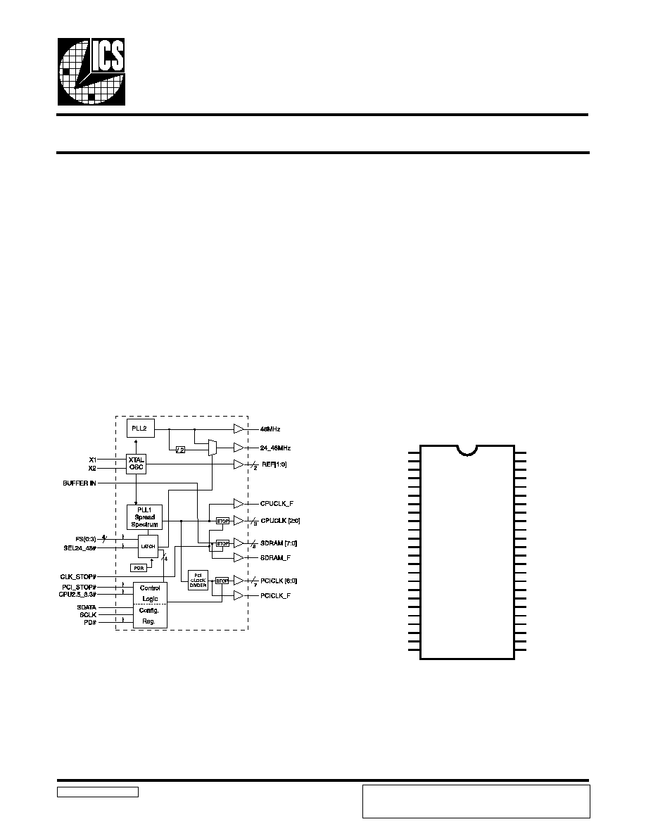
Block Diagram
Pentium is a trademark of Intel Corporation
I
2
C is a trademark of Philips Corporation
Frequency Generator & Integrated Buffers for PENTIUM/Pro
TM
& K6
9248-101 Rev C 2/29/00
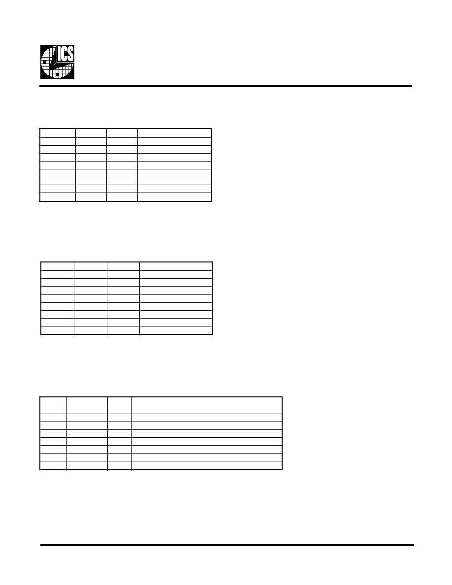
Pin Configuration
Up to 137MHz frequency support
Spread Spectrum for EMI control
Serial I
2
C interface for Power Management,
Frequency Select, Spread Spectrum.
Provides the following system clocks
- 4-CPUs @ 2.5/3.3V, up to 137MHz.
(including CPUCLK_F)
- 9-SDRAMs @3.3V, up to 137MHz
(including SDRAM_F)
- 8-PCI @3.3V, CPU/2 or CPU/3
(including 1 free running PCICLK_F)
- 1-24/48MHz @3.3V
- 1-48MHz @3.3V fixed
- 2-REF @3.3V, 14.318MHz.
Efficient Power management scheme through PCI
and STOP CLOCKS
Spread Spectrum ± .25%, & 0 to -0.5% down spread
48-Pin SSOP and TSSOP
Power Groups
VDDLCPU, GNDLCPU = CPUCLK [2:0], CPUCLK_F
VDDSDR, GNDSDR = SDRAMCLKS [7:0], SDRAM_F
VDDPCI, GNDPCI = PCICLKS [6:0], PCICLK_F
VDD48, GND48 = 48MHz, 24MHz
VDDREF, GNDREF = REF, X1, X2
VDDCOR = PLL CORE
* Internal Pull-up Resistor of 120K to VDD
The ICS9248-101 is the single chip clock solution for
Notebook designs using the 440BX or the VIA Apollo Pro 133
style chipset. It provides all necessary clock signals for such a
system.
Spread spectrum may be enabled through I
2
C programming.
Spread spectrum typically reduces system EMI by 8dB to
10dB. This simplifies EMI qualification without resorting to
board design iterations or costly shielding. The ICS9248-101
employs a proprietary closed loop design, which tightly
controls the percentage of spreading over process and
temperature variations.
VDDREF
REF0
GNDREF
X1
X2
VDDPCI
*CPU2.5_3.3#/PCICLK_F
*FS3/PCICLK0
GNDPCI
*SEL24_48#/PCICLK1
PCICLK2
PCICLK3
PCICLK4
VDDPCI
BUFFER IN
GNDPCI
PCICLK5
PCICLK6
VDDCOR
PCI_STOP#
*PD#
GND48
SDATA
SCLK
REF1/FS2*
VDDLCPU
CPUCLK_F
CPUCLK0
GNDLCPU
CPUCLK1
CPUCLK2
CLK_STOP#
GNDSDR
SDRAM_F
SDRAM0
SDRAM1
VDDSDR
SDRAM2
SDRAM3
GNDSDR
SDRAM4
SDRAM5
VDDSDR
SDRAM6
SDRAM7
VDD48
48MHz/FS0*
24_48MHz/FS1*
ICS9248-101
1
2
3
4
5
6
7
8
9
10
11
12
13
14
15
16
17
18
19
20
21
22
23
24
48
47
46
45
44
43
42
41
40
39
38
37
36
35
34
33
32
31
30
29
28
27
26
25
{
I C
2
ICS reserves the right to make changes in the device data identified in
this publication without further notice. ICS advises its customers to
obtain the latest version of all device data to verify that any
information being relied upon by the customer is current and accurate.
2
ICS9248-101
Pin Descriptions
Notes:
1:
Internal Pull-up Resistor of 120K to 3.3V on indicated inputs
2:
Bidirectional input/output pins, input logic levels are latched at internal power-on-reset. Use 10Kohm resistor
to program logic Hi to VDD or GND for logic low.
N
I
P
R
E
B
M
U
N
E
M
A
N
N
I
P
E
P
Y
T
N
O
I
T
P
I
R
C
S
E
D
1
F
E
R
D
D
V
R
W
P
V
3
.
3
l
a
n
i
m
o
n
,
y
l
p
p
u
s
r
e
w
o
p
L
A
T
X
,
f
e
R
2
0
F
E
R
T
U
O
s
d
a
o
l
S
U
B
A
S
I
r
o
f
r
e
f
f
u
b
R
E
G
N
O
R
T
S
e
h
t
s
i
t
u
p
t
u
o
F
E
R
s
i
h
T
.
k
c
o
l
c
e
c
n
e
r
e
f
e
r
z
h
M
8
1
3
.
4
1
0
2
#
P
O
T
S
_
I
C
P
N
I
)
0
=
E
D
O
M
,
e
d
o
m
e
l
i
b
o
m
n
I
(
w
o
l
t
u
p
n
i
n
e
h
w
,
l
e
v
e
l
0
c
i
g
o
l
t
a
s
k
c
o
l
c
]
0
:
6
[
K
L
C
I
C
P
s
t
l
a
H
,
6
1
,
9
,
3
4
4
,
0
4
,
3
3
D
N
G
R
W
P
d
n
u
o
r
G
4
1
X
N
I
k
c
a
b
d
e
e
f
d
n
a
)
F
p
6
3
(
p
a
c
d
a
o
l
l
a
n
r
e
t
n
i
s
a
h
,
t
u
p
n
i
l
a
t
s
y
r
C
2
X
m
o
r
f
r
o
t
s
i
s
e
r
5
2
X
T
U
O
.
z
H
M
8
1
3
.
4
1
y
l
l
a
n
i
m
o
n
,
t
u
p
t
u
o
l
a
t
s
y
r
C
4
1
,
6
I
C
P
D
D
V
R
W
P
V
3
.
3
l
a
n
i
m
o
n
,
]
0
:
6
[
K
L
C
I
C
P
d
n
a
F
_
K
L
C
I
C
P
r
o
f
y
l
p
p
u
S
7
#
3
.
3
_
5
.
2
U
P
C
2
,
1
N
I
.
t
u
p
n
I
d
e
h
c
t
a
L
.
U
P
C
V
3
.
3
=
W
O
L
,
U
P
C
V
5
.
2
=
h
g
i
H
.
V
3
.
3
r
o
5
.
2
s
i
U
P
C
L
D
D
V
r
e
h
t
e
h
w
s
e
t
a
c
i
d
n
I
F
_
K
L
C
I
C
P
T
U
O
.
t
n
e
m
e
g
a
n
a
m
r
e
w
o
p
r
o
f
#
P
O
T
S
_
I
C
P
y
b
d
e
t
c
e
f
f
a
t
o
n
k
c
o
l
c
I
C
P
g
n
i
n
n
u
r
e
e
r
F
8
3
S
F
2
,
1
N
I
.
t
u
p
n
I
d
e
h
c
t
a
L
.
n
i
p
t
c
e
l
e
s
y
c
n
e
u
q
e
r
F
0
K
L
C
I
C
P
T
U
O
)
y
l
r
a
e
U
P
C
(
w
e
k
s
s
n
4
-
1
h
t
i
w
s
k
c
o
l
c
U
P
C
o
t
s
u
o
n
o
r
h
c
n
y
S
.
t
u
p
t
u
o
k
c
o
l
c
I
C
P
0
1
#
8
4
_
4
2
L
E
S
2
,
1
N
I
z
H
M
8
4
=
w
o
L
n
e
h
w
z
H
M
8
4
r
o
4
2
r
e
h
t
i
e
s
t
c
e
l
e
S
1
K
L
C
I
C
P
T
U
O
)
y
l
r
a
e
U
P
C
(
w
e
k
s
s
n
4
-
1
h
t
i
w
s
k
c
o
l
c
U
P
C
o
t
s
u
o
n
o
r
h
c
n
y
S
.
t
u
p
t
u
o
k
c
o
l
c
I
C
P
,
3
1
,
7
1
,
8
1
,
1
1
,
2
1
]
2
:
6
[
K
L
C
I
C
P
T
U
O
)
y
l
r
a
e
U
P
C
(
w
e
k
s
s
n
4
-
1
h
t
i
w
s
k
c
o
l
c
U
P
C
o
t
s
u
o
n
o
r
h
c
n
y
S
.
s
t
u
p
t
u
o
k
c
o
l
c
I
C
P
5
1
N
I
R
E
F
F
U
B
N
I
.
s
t
u
p
t
u
o
M
A
R
D
S
r
o
f
s
r
e
f
f
u
B
t
u
o
n
a
F
o
t
t
u
p
n
I
9
1
R
O
C
D
D
V
R
W
P
V
3
.
3
.
e
r
o
c
L
L
P
e
h
t
r
o
f
n
i
p
r
e
w
o
P
1
2
#
D
P
1
N
I
e
h
T
.
e
t
a
t
s
r
e
w
o
p
w
o
l
a
o
t
n
i
e
c
i
v
e
d
e
h
t
n
w
o
d
r
e
w
o
p
o
t
d
e
s
u
n
i
p
t
u
p
n
i
w
o
l
e
v
i
t
c
a
s
u
o
n
o
r
h
c
n
y
s
A
r
e
w
o
p
e
h
t
f
o
y
c
n
e
t
a
l
e
h
T
.
d
e
p
p
o
t
s
e
r
a
l
a
t
s
y
r
c
e
h
t
d
n
a
O
C
V
e
h
t
d
n
a
d
e
l
b
a
s
i
d
e
r
a
s
k
c
o
l
c
l
a
n
r
e
t
n
i
.
s
m
4
n
a
h
t
r
e
t
a
e
r
g
e
b
t
o
n
l
l
i
w
n
w
o
d
2
2
8
4
D
N
G
R
W
P
.
e
r
o
c
L
L
P
d
e
x
i
f
&
s
r
e
f
f
u
b
t
u
p
t
u
o
z
H
M
8
4
&
4
2
e
h
t
r
o
f
n
i
p
d
n
u
o
r
G
,
2
3
,
1
3
,
9
2
,
8
2
8
3
,
7
3
,
5
3
,
4
3
]
0
:
7
[
M
A
R
D
S
T
U
O
.
)
t
e
s
p
i
h
c
y
b
d
e
l
l
o
r
t
n
o
c
(
n
i
p
N
I
R
E
F
F
U
B
m
o
r
f
s
t
u
p
t
u
o
r
e
f
f
u
B
t
u
o
n
a
F
,
s
t
u
p
t
u
o
k
c
o
l
c
M
A
R
D
S
6
3
,
0
3
R
D
S
D
D
V
R
W
P
.
V
3
.
3
l
a
n
i
m
o
n
,
e
r
o
C
L
L
P
U
P
C
d
n
a
]
0
:
7
[
M
A
R
D
S
r
o
f
y
l
p
p
u
S
3
2
A
T
A
D
S
N
I
I
r
o
f
t
u
p
n
i
a
t
a
D
2
t
u
p
n
i
t
n
a
r
e
l
o
t
V
5
,
t
u
p
n
i
l
a
i
r
e
s
C
4
2
K
L
C
S
N
I
I
f
o
t
u
p
n
i
k
c
o
l
C
2
t
u
p
n
i
t
n
a
r
e
l
o
t
V
5
,
t
u
p
n
i
C
5
2
z
H
M
8
4
_
4
2
T
U
O
0
1
n
i
p
y
b
e
l
b
a
t
c
e
l
e
s
k
c
o
l
c
t
u
p
t
u
o
z
H
M
8
4
r
o
z
H
M
4
2
1
S
F
2
,
1
N
I
.
t
u
p
n
I
d
e
h
c
t
a
L
.
n
i
p
t
c
e
l
e
s
y
c
n
e
u
q
e
r
F
6
2
z
H
M
8
4
T
U
O
k
c
o
l
c
t
u
p
t
u
o
z
H
M
8
4
0
S
F
2
,
1
N
I
t
u
p
n
I
d
e
h
c
t
a
L
.
n
i
p
t
c
e
l
e
s
y
c
n
e
u
q
e
r
F
7
2
8
4
D
D
V
R
W
P
.
e
r
o
c
L
L
P
d
e
x
i
f
d
n
a
s
r
e
f
f
u
b
t
u
p
t
u
o
z
H
M
8
4
&
4
2
r
o
f
r
e
w
o
P
9
3
F
_
M
A
R
D
S
T
U
O
#
P
O
T
S
_
U
P
C
y
b
d
e
t
c
e
f
f
a
t
o
N
.
t
u
p
t
u
o
k
c
o
l
c
M
A
R
D
S
g
n
i
n
n
u
r
e
e
r
F
1
4
#
P
O
T
S
_
K
L
C
N
I
.
w
o
l
n
e
v
i
r
d
n
e
h
w
l
e
v
e
l
"
0
"
c
i
g
o
l
t
a
)
7
:
0
(
M
A
R
D
S
&
,
)
2
:
0
(
K
L
C
U
P
C
s
t
l
a
h
t
u
p
n
i
s
u
o
n
o
r
h
c
n
y
s
a
s
i
h
T
5
4
,
3
4
,
2
4
]
0
:
2
[
K
L
C
U
P
C
T
U
O
U
P
C
L
D
D
V
y
b
d
e
r
e
w
o
p
,
s
t
u
p
t
u
o
k
c
o
l
c
U
P
C
6
4
F
_
K
L
C
U
P
C
T
U
O
#
P
O
T
S
_
U
P
C
e
h
t
y
b
d
e
t
c
e
f
f
a
t
o
N
.
k
c
o
l
c
U
P
C
g
n
i
n
n
u
r
e
e
r
F
7
4
U
P
C
L
D
D
V
R
W
P
V
5
.
2
s
k
c
o
l
c
U
P
C
r
o
f
y
l
p
p
u
S
8
4
1
F
E
R
T
U
O
.
k
c
o
l
c
e
c
n
e
r
e
f
e
r
z
H
M
8
1
3
.
4
1
2
S
F
2
,
1
N
I
t
u
p
n
I
d
e
h
c
t
a
L
.
n
i
p
t
c
e
l
e
s
y
c
n
e
u
q
e
r
F
3
ICS9248-101
1.
The ICS clock generator is a slave/receiver, I
2
C component. It can read back the data stored in the latches for verification.
Read-Back will support Intel PIIX4 "Block-Read" protocol.
2.
The data transfer rate supported by this clock generator is 100K bits/sec or less (standard mode)
3.
The input is operating at 3.3V logic levels.
4.
The data byte format is 8 bit bytes.
5.
To simplify the clock generator I
2
C interface, the protocol is set to use only "Block-Writes" from the controller. The
bytes must be accessed in sequential order from lowest to highest byte with the ability to stop after any complete byte
has been transferred. The Command code and Byte count shown above must be sent, but the data is ignored for those
two bytes. The data is loaded until a Stop sequence is issued.
6.
At power-on, all registers are set to a default condition, as shown.
General I
2
C serial interface information
The information in this section assumes familiarity with I
2
C programming.
For more information, contact ICS for an I
2
C programming application note.
How to Write:
Controller (host) sends a start bit.
Controller (host) sends the write address D2
(H)
ICS clock will acknowledge
Controller (host) sends a dummy command code
ICS clock will acknowledge
Controller (host) sends a dummy byte count
ICS clock will acknowledge
Controller (host) starts sending first byte (Byte 0)
through byte 5
ICS clock will acknowledge each byte one at a time.
Controller (host) sends a Stop bit
How to Read:
Controller (host) will send start bit.
Controller (host) sends the read address D3
(H)
ICS clock will acknowledge
ICS clock will send the byte count
Controller (host) acknowledges
ICS clock sends first byte (Byte 0) through byte 5
Controller (host) will need to acknowledge each byte
Controller (host) will send a stop bit
Notes:
Controller (Host)
ICS (Slave/Receiver)
Start Bit
Address
D3
(H)
ACK
Byte Count
ACK
Byte 0
ACK
Byte 1
ACK
Byte 2
ACK
Byte 3
ACK
Byte 4
ACK
Byte 5
ACK
Stop Bit
How to Read:
Controller (Host)
ICS (Slave/Receiver)
Start Bit
Address
D2
(H)
ACK
Dummy Command Code
ACK
Dummy Byte Count
ACK
Byte 0
ACK
Byte 1
ACK
Byte 2
ACK
Byte 3
ACK
Byte 4
ACK
Byte 5
ACK
Stop Bit
How to Write:
4
ICS9248-101
Functionality
V
DD
= 3.3V±5%, V
DDL
= 2.5V±5% or 3.3±5%, TA=0 to 70°C
Crystal (X1, X2) = 14.31818MHz
3
S
F
2
S
F
1
S
F
0
S
F
U
P
C
)
z
H
M
(
I
C
P
)
z
H
M
(
0
0
0
0
0
0
.
4
2
1
3
3
.
1
4
0
0
0
1
0
0
.
0
2
1
0
0
.
0
4
0
0
1
0
9
9
.
4
1
1
3
3
.
8
3
0
0
1
1
9
9
.
9
0
1
6
6
.
6
3
0
1
0
0
0
0
.
5
0
1
0
0
.
5
3
0
1
0
1
1
3
.
3
8
5
6
.
1
4
0
1
1
0
0
0
.
7
3
1
5
2
.
4
3
0
1
1
1
0
0
.
5
7
0
5
.
7
3
1
0
0
0
0
0
.
0
0
1
3
3
.
3
3
1
0
0
1
0
0
.
5
9
7
6
.
1
3
1
0
1
0
1
3
.
3
8
7
7
.
7
2
1
0
1
1
3
3
.
3
3
1
3
3
.
3
3
1
1
0
0
0
0
.
0
9
0
0
.
0
3
1
1
0
1
2
2
.
6
9
7
0
.
2
3
1
1
1
0
2
8
.
6
6
1
4
.
3
3
1
1
1
1
5
.
1
9
5
.
0
3
Byte0: Functionality and Frequency Select Register (default = 0)
Serial Configuration Command Bitmap
t
i
B
n
o
i
t
p
i
r
c
s
e
D
D
W
P
7
t
i
B
d
a
e
r
p
S
r
e
t
n
e
C
,
n
o
i
t
a
l
u
d
o
M
m
u
r
t
c
e
p
S
d
a
e
r
p
S
%
5
2
.
0
±
-
0
d
a
e
r
p
S
n
w
o
D
%
5
.
0
-
o
t
0
-
1
1
t
i
B
]
4
:
6
,
2
[
]
4
:
6
,
2
[
t
i
B
K
L
C
U
P
C
)
z
H
M
(
K
L
C
I
C
P
)
z
H
M
(
1
e
t
o
N
0
0
0
0
0
0
.
4
2
1
3
3
.
1
4
1
0
0
0
0
0
.
0
2
1
0
0
.
0
4
0
1
0
0
9
9
.
4
1
1
3
3
.
8
3
1
1
0
0
9
9
.
9
0
1
6
6
.
6
3
0
0
1
0
0
0
.
5
0
1
0
0
.
5
3
1
0
1
0
1
3
.
3
8
5
6
.
1
4
0
1
1
0
0
0
.
7
3
1
5
2
.
4
3
1
1
1
0
0
0
.
5
7
0
5
.
7
3
0
0
0
1
0
0
.
0
0
1
3
3
.
3
3
1
0
0
1
0
0
.
5
9
7
6
.
1
3
0
1
0
1
1
3
.
3
8
7
7
.
7
2
1
1
0
1
3
3
.
3
3
1
3
3
.
3
3
0
0
1
1
0
0
.
0
9
0
0
.
0
3
1
0
1
1
2
2
.
6
9
7
0
.
2
3
0
1
1
1
2
8
.
6
6
1
4
.
3
3
1
1
1
1
5
.
1
9
5
.
0
3
3
t
i
B
s
t
u
p
n
i
d
e
h
c
t
a
l
,
t
c
e
l
e
s
e
r
a
w
d
r
a
h
y
b
d
e
t
c
e
l
e
s
s
i
y
c
n
e
u
q
e
r
F
-
0
]
4
:
6
,
2
[
t
i
B
y
b
d
e
t
c
e
l
e
s
s
i
y
c
n
e
u
q
e
r
F
-
1
0
1
t
i
B
l
a
m
r
o
N
-
0
d
e
l
b
a
n
E
m
u
r
t
c
e
p
S
d
a
e
r
p
S
-
1
1
0
t
i
B
g
n
i
n
n
u
R
-
0
s
t
u
p
t
u
o
l
l
a
e
t
a
t
s
i
r
T
-
1
0
Notes:
1, Default at Power-up will be for latched
logic inputs to define frequency. Bit [2,
6:4] are default to 0010.
2, PWD = Power-Up Default
3, When disabling spread spectrum bit7
needs to be set to 0 to maintain nominal
frequency.
5
ICS9248-101
Notes:
1. Inactive means outputs are held LOW and are disabled from switching.
2. Latched Frequency Selects (FS#) will be inverted logic load of the input frequency select pin conditions.
Byte 2: PCI Active/Inactive Register (1 = enable, 0 = disable)
t
i
B
#
n
i
P
D
W
P
n
o
i
t
p
i
r
c
s
e
D
7
t
i
B
7
1
)
t
c
a
n
I
/
t
c
A
(
F
_
K
L
C
I
C
P
6
t
i
B
8
1
1
)
t
c
a
n
I
/
t
c
A
(
6
K
L
C
I
C
P
5
t
i
B
7
1
1
)
t
c
a
n
I
/
t
c
A
(
5
K
L
C
I
C
P
4
t
i
B
3
1
1
)
t
c
a
n
I
/
t
c
A
(
4
K
L
C
I
C
P
3
t
i
B
2
1
1
)
t
c
a
n
I
/
t
c
A
(
3
K
L
C
I
C
P
2
t
i
B
1
1
1
)
t
c
a
n
I
/
t
c
A
(
2
K
L
C
I
C
P
1
t
i
B
0
1
1
)
t
c
a
n
I
/
t
c
A
(
1
K
L
C
I
C
P
0
t
i
B
8
1
)
t
c
a
n
I
/
t
c
A
(
0
K
L
C
I
C
P
Byte 1: CPU, Active/Inactive Register (1 = enable, 0 = disable)
t
i
B
#
n
i
P
D
W
P
n
o
i
t
p
i
r
c
s
e
D
7
t
i
B
-
1
)
d
e
v
r
e
s
e
R
(
6
t
i
B
6
4
1
)
t
c
a
n
I
/
t
c
A
(
F
_
K
L
C
U
P
C
5
t
i
B
-
1
)
d
e
v
r
e
s
e
R
(
4
t
i
B
-
1
)
d
e
v
r
e
s
e
R
(
3
t
i
B
9
3
1
)
t
c
a
n
I
/
t
c
A
(
F
_
M
A
R
D
S
2
t
i
B
2
4
1
)
t
c
a
n
I
/
t
c
A
(
2
K
L
C
U
P
C
1
t
i
B
3
4
1
)
t
c
a
n
I
/
t
c
A
(
1
K
L
C
U
P
C
0
t
i
B
5
4
1
)
t
c
a
n
I
/
t
c
A
(
0
K
L
C
U
P
C
Byte 3: SDRAM Active/Inactive Register (1 = enable, 0 = disable)
t
i
B
#
n
i
P
D
W
P
n
o
i
t
p
i
r
c
s
e
D
7
t
i
B
-
1
)
d
e
v
r
e
s
e
R
(
6
t
i
B
-
1
)
d
e
v
r
e
s
e
R
(
5
t
i
B
-
1
)
d
e
v
r
e
s
e
R
(
4
t
i
B
-
1
)
d
e
v
r
e
s
e
R
(
3
t
i
B
8
2
1
)
e
v
i
t
c
a
n
I
/
e
v
i
t
c
A
(
7
M
A
R
D
S
2
t
i
B
9
2
1
)
e
v
i
t
c
a
n
I
/
e
v
i
t
c
A
(
6
M
A
R
D
S
1
t
i
B
1
3
1
)
e
v
i
t
c
a
n
I
/
e
v
i
t
c
A
(
5
M
A
R
D
S
0
t
i
B
2
3
1
)
e
v
i
t
c
a
n
I
/
e
v
i
t
c
A
(
4
M
A
R
D
S