Äîêóìåíòàöèÿ è îïèñàíèÿ www.docs.chipfind.ru
ICS9248-135
Third party brands and names are the property of their respective owners.
Integrated
Circuit
Systems, Inc.
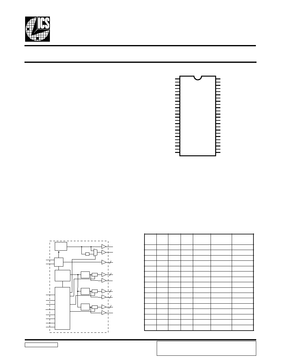
Block Diagram
9248-135 Rev A 1/16/01
Recommended Application:
Motherboard Single chip clock solution for SIS540,
SIS630 Pentium II/III and K6 chipsets.
Output Features:
·
3- CPUs @ 2.5/3.3V, up to 166MHz.
·
10 - SDRAM @ 3.3V, up to 166MHz
including 2 SDRAM_F's
·
7- PCI @3.3V,
·
1- 48MHz, @3.3V fixed.
·
1- 24/48MHz, @3.3V selectable by I
2
C
(Default is 24MHz).
·
2- REF @3.3V, 14.318MHz.
Features:
·
Up to 166MHz frequency support
·
Support FS0-FS3 trapping status bit for I
2
C read back.
·
Support power management: CPU, PCI, SDRAM stop
and Power down Mode form I
2
C programming.
·
Spread spectrum for EMI control (0 to -0.5%, ± 0.25%).
·
FS0, FS1, FS3 must have a internal 120K pull-Down
to GND.
·
Uses external 14.318MHz crystal
Skew Specifications:
·
CPU - CPU: < 175ps
·
SDRAM - SDRAM < 250ps
·
PCI - PCI: < 500ps
·
CPU - SDRAM: < 500ps
·
CPU (early) - PCI: 1-4ns (typ. 2ns)
Functionality
Pin Configuration
48-Pin 300mil SSOP
* These inputs have a 120K pull down to GND.
** These inputs have a 120K pullup to VDD.
1 These are double strength.
VDDREF
* REF0/FS3
GNDREF
X1
X2
VDDPCI
*PCICLK_F/FS1
*PCICLK1/FS2
PCICLK2
GNDPCI
PCICLK3
PCICLK4
PCICLK5
PCICLK6
VDD
GND
SDRAM_STOP#
**PD#
VDD
CPU_STOP#
PCI_STOP#
GND
SDATA
SCLK
1
REF1
VDDLCPU
CPUCLK_F
CPUCLK1
GNDL
CPUCLK2
VDD
SDRAM_F1
SDRAM_F0
GND
SDRAM7
SDRAM6
VDD
SDRAM5
SDRAM4
GND
SDRAM3
SDRAM2
VDD
SDRAM1
SDRAM0
VDD
48MHz/FS0*
24_48MHz/CPU2.5_3.3#*
1
ICS9248-135
1
2
3
4
5
6
7
8
9
10
11
12
13
14
15
16
17
18
19
20
21
22
23
24
48
47
46
45
44
43
42
41
40
39
38
37
36
35
34
33
32
31
30
29
28
27
26
25
Frequency Generator & Integrated Buffers for Celeron & PII/III
TM
& K6
CPU2.5_3.3#
PLL2
PLL1
Spread
Spectrum
48MHz
24_48MHz
CPUCLK [2:1]
SDRAM [7:0]
PCICLK [6:1]
SDRAM_F [1:0]
CPUCLK_F
PCICLK_F
6
2
2
2
8
X1
X2
XTAL
OSC
CPU
DIVDER
SDRAM
DIVDER
PCI
DIVDER
Stop
Stop
Stop
SDATA
SCLK
FS[3:0]
PD#
PCI_STOP#
CPU_STOP#
SDRAM_STOP#
Control
Logic
Config.
Reg.
/ 2
REF[1:0]
3
S
F
2
S
F
1
S
F
0
S
F
U
P
C
)
z
H
M
(
M
A
R
D
S
)
z
H
M
(
K
L
C
I
C
P
)
z
H
M
(
0
0
0
0
6
.
6
6
0
.
0
0
1
3
.
3
3
0
0
0
1
0
.
0
0
1
0
.
0
0
1
3
.
3
3
0
0
1
0
0
.
0
5
1
0
.
0
0
1
5
.
7
3
0
0
1
1
3
.
3
3
1
0
.
0
0
1
3
.
3
3
0
1
0
0
8
.
6
6
6
.
3
3
1
4
.
3
3
0
1
0
1
0
.
0
0
1
3
.
3
3
1
3
.
3
3
0
1
1
0
0
.
0
0
1
0
.
0
5
1
5
.
7
3
0
1
1
1
3
.
3
3
1
3
.
3
3
1
3
.
3
3
1
0
0
0
8
.
6
6
8
.
6
6
4
.
3
3
1
0
0
1
0
.
7
9
0
.
7
9
3
.
2
3
1
0
1
0
0
.
0
7
0
.
5
0
1
0
.
5
3
1
0
1
1
0
.
5
9
0
.
5
9
7
.
1
3
1
1
0
0
0
.
5
9
7
.
6
2
1
7
.
1
3
1
1
0
1
0
.
2
1
1
0
.
2
1
1
3
.
7
3
1
1
1
0
0
.
7
9
3
.
9
2
1
2
.
2
3
1
1
1
1
2
.
6
9
2
.
6
9
1
.
2
3
ICS reserves the right to make changes in the device data identified in
this publication without further notice. ICS advises its customers to
obtain the latest version of all device data to verify that any
information being relied upon by the customer is current and accurate.
2
ICS9248-135
Third party brands and names are the property of their respective owners.
The ICS9248-135 is the single chip clock solution for Desktop/Notebook designs using the SIS 540/630 style chipset. It
provides all necessary clock signals for such a system.
Spread spectrum may be enabled through I
2
C programming. Spread spectrum typically reduces system EMI by 8dB to
10dB. This simplifies EMI qualification without resorting to board design iterations or costly shielding. The ICS9248-135
employs a proprietary closed loop design, which tightly controls the percentage of spreading over process and temperature
variations.
Serial programming I
2
C interface allows changing functions, stop clock programming and frequency selection.
General Description
Pin Configuration
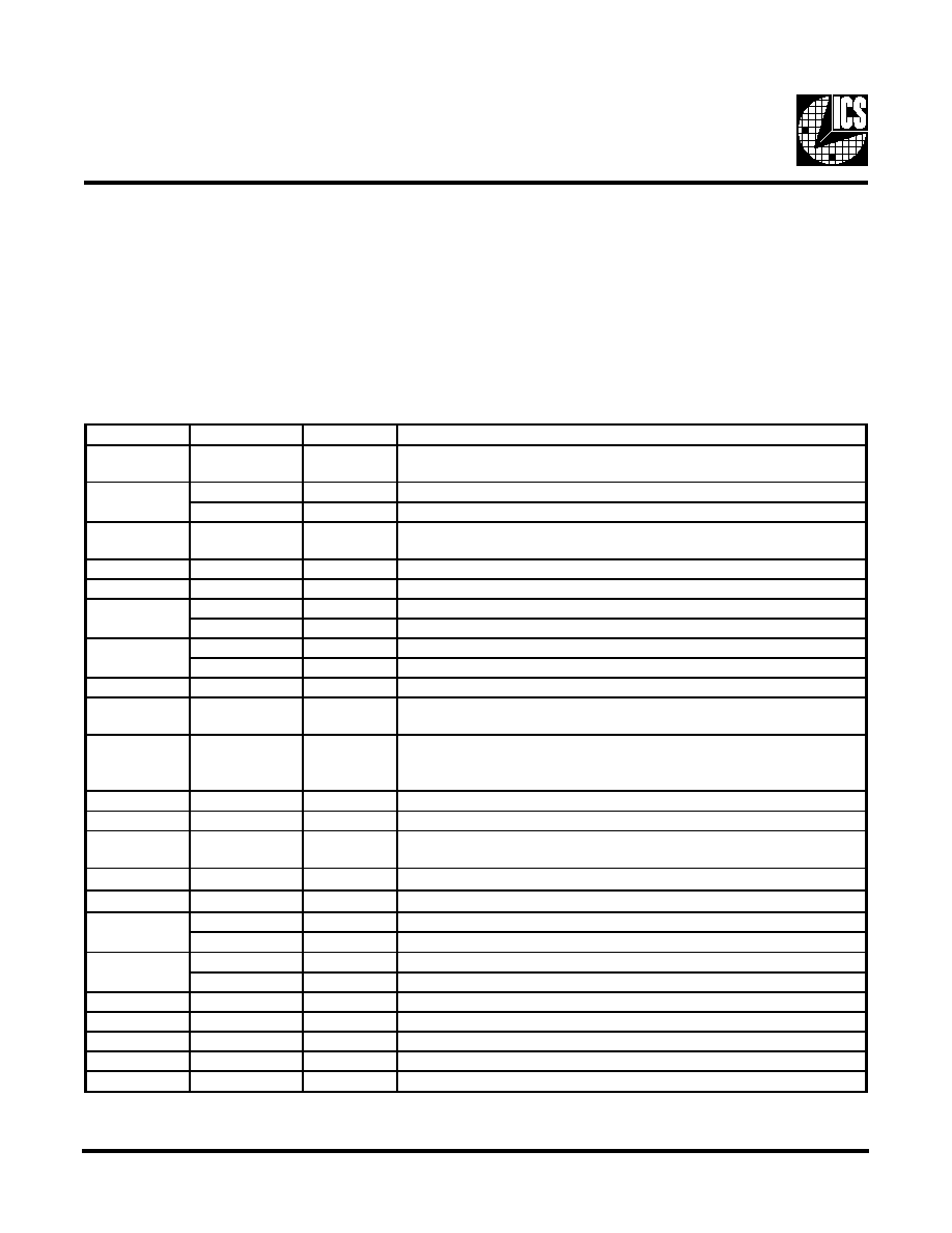
PIN NUMBER
PIN NAME
TYPE
DESCRIPTION
1, 6, 15, 19, 27,
30, 36, 42
VDD
PWR
3.3V Power supply for SDRAM output buffers, PCI output buffers, reference
output buffers and 48MHz output
REF0
OUT
14.318 MHz reference clock.
FS3
IN
Frequency select pin.
3, 10, 16, 22, 33,
39, 44
GND
PWR
Ground pin for 3V outputs.
4
X1
IN
Crystal input,nominally 14.318MHz.
5
X2
OUT
Crystal output, nominally 14.318MHz.
FS1
IN
Frequency select pin.
PCICLK_F
OUT
Free running PCICLK clock output. Not affected by PCI_STOP#
FS2
IN
Frequency select pin.
PCICLK1
OUT
PCI clock outputs.
14, 13, 12, 11, 9
PCICLK (6:2)
OUT
PCI clock outputs.
17
SDRAM_STOP#
IN
Stops all SDRAMs besides the SDRAM_F clocks at logic 0 level, when input low
18
PD#
IN
Asynchronous active low input pin used to power down the device into a low
power state. The internal clocks are disabled and the VCO and the crystal are
stopped. The latency of the power down will not be greater than 3ms.
20
CPU_STOP#
IN
Stops all CPUCLKs clocks at logic 0 level, when input low
21
PCI_STOP#
IN
Stops all PCICLKs clocks at logic 0 level, when input low
38, 37, 35, 34,
32, 31, 29, 28
SDRAM (7:0)
OUT
SDRAM clock outputs
23
SDATA
IN
Data input for I
2
C serial input, 5V tolerant input
24
SCLK
IN
Clock input of I
2
C input, 5V tolerant input
CPU2.5_3.3#
IN
Voltage select 2.5V when high - 3.3V when low
24_48MHz
OUT
Clock output for super I/O/USB default is 24MHz
FS0
IN
Frequency select pin.
48MHz
OUT
48MHz output clock
41, 40
SDRAM_F (1:0)
OUT
Free running SDRAM clock outputs. Not affected by SDRAM_STOP#
45, 43
CPUCLK (1:2)
OUT
CPU clock outputs.
46
CPUCLK_F
OUT
Free running CPUCLK clock output. Not affected by CPU_STOP#
47
VDDLCPU
PWR
Power pin for the CPUCLKs. 2.5V
48
REF1
OUT
14.318 MHz reference clock.
26
2
7
8
25
3
ICS9248-135
Third party brands and names are the property of their respective owners.
1.
The ICS clock generator is a slave/receiver, I
2
C component. It can read back the data stored in the latches for
verification. Read-Back will support Intel PIIX4 "Block-Read" protocol.
2.
The data transfer rate supported by this clock generator is 100K bits/sec or less (standard mode)
3.
The input is operating at 3.3V logic levels.
4.
The data byte format is 8 bit bytes.
5.
To simplify the clock generator I
2
C interface, the protocol is set to use only "Block-Writes" from the controller. The
bytes must be accessed in sequential order from lowest to highest byte with the ability to stop after any complete byte
has been transferred. The Command code and Byte count shown above must be sent, but the data is ignored for those
two bytes. The data is loaded until a Stop sequence is issued.
6.
At power-on, all registers are set to a default condition, as shown.
General I
2
C serial interface information
The information in this section assumes familiarity with I
2
C programming.
For more information, contact ICS for an I
2
C programming application note.
How to Write:
· Controller (host) sends a start bit.
· Controller (host) sends the write address D2
(H)
· ICS clock will acknowledge
· Controller (host) sends a dummy command code
· ICS clock will acknowledge
· Controller (host) sends a dummy byte count
· ICS clock will acknowledge
· Controller (host) starts sending first byte (Byte 0)
through byte 5
· ICS clock will acknowledge each byte one at a time.
· Controller (host) sends a Stop bit
How to Read:
· Controller (host) will send start bit.
· Controller (host) sends the read address D3
(H)
· ICS clock will acknowledge
· ICS clock will send the byte count
· Controller (host) acknowledges
· ICS clock sends first byte (Byte 0) through byte 5
· Controller (host) will need to acknowledge each byte
· Controller (host) will send a stop bit
Notes:
Controller (Host)
ICS (Slave/Receiver)
Start Bit
Address
D3
(H)
ACK
Byte Count
ACK
Byte 0
ACK
Byte 1
ACK
Byte 2
ACK
Byte 3
ACK
Byte 4
ACK
Byte 5
ACK
Stop Bit
How to Read:
Controller (Host)
ICS (Slave/Receiver)
Start Bit
Address
D2
(H)
ACK
Dummy Command Code
ACK
Dummy Byte Count
ACK
Byte 0
ACK
Byte 1
ACK
Byte 2
ACK
Byte 3
ACK
Byte 4
ACK
Byte 5
ACK
Stop Bit
How to Write:
4
ICS9248-135
Third party brands and names are the property of their respective owners.
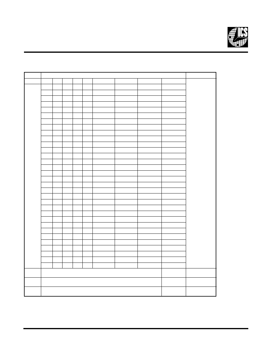
Byte0: Functionality and Frequency Select Register (default = 0)
Serial Configuration Command Bitmap
Note: PWD = Power-Up Default
Note1:
Default at power-up will be for latched logic inputs to define frequency, as displayed by Bit 3.
The I
2
C readback for Bits 7, 2, 6:4 indicate the revision code.
I
2
C is a trademark of Philips Corporation
t
i
B
n
o
i
t
p
i
r
c
s
e
D
D
W
P
7
t
i
B
2
t
i
B
6
t
i
B
5
t
i
B
4
t
i
B
U
P
C
M
A
R
D
S
I
C
P
S
S
0
1
0
0
0
1
e
t
o
N
,
2
,
7
t
i
B
4
:
6
t
i
B
0
0
0
0
0
6
.
6
6
0
.
0
0
1
3
.
3
3
%
5
.
0
-
o
t
0
0
0
0
0
1
0
.
0
0
1
0
.
0
0
1
3
.
3
3
%
5
.
0
-
o
t
0
0
0
0
1
0
0
.
0
5
1
0
.
0
0
1
5
.
7
3
%
5
2
.
0
±
0
0
0
1
1
3
.
3
3
1
0
.
0
0
1
3
.
3
3
%
5
.
0
-
o
t
0
0
0
1
0
0
8
.
6
6
6
.
3
3
1
4
.
3
3
%
5
.
0
-
o
t
0
0
0
1
0
1
0
.
0
0
1
3
.
3
3
1
3
.
3
3
%
5
.
0
-
o
t
0
0
0
1
1
0
0
.
0
0
1
0
.
0
5
1
5
.
7
3
%
5
2
.
0
±
0
0
1
1
1
3
.
3
3
1
3
.
3
3
1
3
.
3
3
%
5
.
0
-
o
t
0
0
1
0
0
0
8
.
6
6
8
.
6
6
4
.
3
3
%
5
2
.
0
±
0
1
0
0
1
0
.
7
9
0
.
7
9
3
.
2
3
%
5
.
0
-
o
t
0
0
1
0
1
0
0
.
0
7
0
.
5
0
1
0
.
5
3
%
5
2
.
0
±
0
1
0
1
1
0
.
5
9
0
.
5
9
7
.
1
3
%
5
2
.
0
±
0
1
1
0
0
0
.
5
9
7
.
6
2
1
7
.
1
3
%
5
2
.
0
±
0
1
1
0
1
0
.
2
1
1
0
.
2
1
1
3
.
7
3
%
5
2
.
0
±
0
1
1
1
0
0
.
7
9
3
.
9
2
1
3
.
2
3
%
5
.
0
-
o
t
0
0
1
1
1
1
2
.
6
9
2
.
6
9
1
.
2
3
%
5
.
0
-
o
t
0
1
0
0
0
0
8
.
6
6
2
.
0
0
1
4
.
3
3
%
5
2
.
0
±
1
0
0
0
1
2
.
0
0
1
2
.
0
0
1
4
.
3
3
%
5
2
.
0
±
1
0
0
1
0
0
.
6
6
1
7
.
0
1
1
7
.
7
2
%
5
2
.
0
±
1
0
0
1
1
2
.
0
0
1
6
.
3
3
1
4
.
3
3
%
5
2
.
0
±
1
0
1
0
0
0
.
5
7
0
.
0
0
1
5
.
7
3
%
5
2
.
0
±
1
0
1
0
1
3
.
3
8
0
.
5
2
1
3
.
1
3
%
5
2
.
0
±
1
0
1
1
0
0
.
5
0
1
0
.
0
4
1
0
.
5
3
%
5
2
.
0
±
1
0
1
1
1
6
.
3
3
1
6
.
3
3
1
4
.
3
3
%
5
2
.
0
±
1
1
0
0
0
3
.
0
1
1
0
.
7
4
1
8
.
6
3
%
5
2
.
0
±
1
1
0
0
1
0
.
5
1
1
3
.
3
5
1
3
.
8
3
%
5
2
.
0
±
1
1
0
1
0
0
.
0
2
1
0
.
0
2
1
0
.
0
3
%
5
2
.
0
±
1
1
0
1
1
0
.
8
3
1
0
.
8
3
1
5
.
4
3
%
5
2
.
0
±
1
1
1
0
0
0
.
0
4
1
0
.
0
4
1
0
.
5
3
%
5
2
.
0
±
1
1
1
0
1
0
.
5
4
1
0
.
5
4
1
3
.
6
3
%
5
2
.
0
±
1
1
1
1
0
5
.
7
4
1
5
.
7
4
1
9
.
6
3
%
5
2
.
0
±
1
1
1
1
1
0
.
0
6
1
0
.
0
6
1
7
.
6
2
%
5
2
.
0
±
3
t
i
B
s
t
u
p
n
I
d
e
h
c
t
a
L
,
t
c
e
l
e
s
e
r
a
w
d
r
a
h
y
b
d
e
t
c
e
l
e
s
s
i
y
c
n
e
u
q
e
r
F
-
0
4
:
6
,
2
,
7
t
i
B
y
b
d
e
t
c
e
l
e
s
s
i
y
c
n
e
u
q
e
r
F
-
1
0
1
t
i
B
l
a
m
r
o
N
-
0
d
e
l
b
a
n
E
m
u
r
t
c
e
p
S
d
a
e
r
p
S
-
1
1
0
t
i
B
g
n
i
n
n
u
R
-
0
s
t
u
p
t
u
o
l
l
a
e
t
a
t
s
i
r
T
-
1
0
5
ICS9248-135
Third party brands and names are the property of their respective owners.
Byte 1: CPU, Active/Inactive Register
(1= enable, 0 = disable)
Notes:
1. Inactive means outputs are held LOW and are disabled
from switching.
2. Latched Frequency Selects (FS#) will be inverted logic
load of the input frequency select pin conditions.
Byte 4: Reserved , Active/Inactive Register
(1= enable, 0 = disable)
Byte 3: SDRAM, Active/Inactive Register
(1= enable, 0 = disable)
T
I
B
#
N
I
P
D
W
P
N
O
I
T
P
I
R
C
S
E
D
7
t
i
B
-
1
#
8
4
_
4
2
L
E
S
)
0
o
t
t
e
s
n
e
h
w
z
H
M
8
4
(
)
1
o
t
t
e
s
n
e
h
w
z
H
M
4
2
(
6
t
i
B
-
1
d
e
v
r
e
s
e
R
5
t
i
B
-
1
d
e
v
r
e
s
e
R
4
t
i
B
-
1
d
e
v
r
e
s
e
R
3
t
i
B
3
4
1
)
t
c
a
n
I
/
t
c
A
(
2
K
L
C
U
P
C
2
t
i
B
5
4
1
)
t
c
a
n
I
/
t
c
A
(
1
K
L
C
U
P
C
1
t
i
B
6
4
1
)
t
c
a
n
I
/
t
c
A
(
0
K
L
C
U
P
C
0
t
i
B
-
1
d
e
v
r
e
s
e
R
T
I
B
#
N
I
P
D
W
P
N
O
I
T
P
I
R
C
S
E
D
7
t
i
B
5
2
1
z
H
M
8
4
_
4
2
6
t
i
B
6
2
1
z
H
M
8
4
5
t
i
B
1
4
1
1
F
_
M
A
R
D
S
4
t
i
B
0
4
1
0
F
_
M
A
R
D
S
3
t
i
B
8
3
1
7
M
A
R
D
S
2
t
i
B
7
3
1
6
M
A
R
D
S
1
t
i
B
5
3
1
5
M
A
R
D
S
0
t
i
B
4
3
1
4
M
A
R
D
S
T
I
B
#
N
I
P
D
W
P
N
O
I
T
P
I
R
C
S
E
D
7
t
i
B
2
3
1
)
t
c
a
n
I
/
t
c
A
(
3
M
A
R
D
S
6
t
i
B
1
3
1
)
t
c
a
n
I
/
t
c
A
(
2
M
A
R
D
S
5
t
i
B
9
2
1
)
t
c
a
n
I
/
t
c
A
(
1
M
A
R
D
S
4
t
i
B
8
2
1
)
t
c
a
n
I
/
t
c
A
(
0
M
A
R
D
S
3
t
i
B
-
1
d
e
v
r
e
s
e
R
2
t
i
B
-
1
d
e
v
r
e
s
e
R
1
t
i
B
-
1
d
e
v
r
e
s
e
R
0
t
i
B
-
1
d
e
v
r
e
s
e
R
T
I
B
#
N
I
P
D
W
P
N
O
I
T
P
I
R
C
S
E
D
7
t
i
B
-
0
)
e
t
o
N
(
d
e
v
r
e
s
e
R
6
t
i
B
-
0
)
e
t
o
N
(
d
e
v
r
e
s
e
R
5
t
i
B
-
0
)
e
t
o
N
(
d
e
v
r
e
s
e
R
4
t
i
B
-
0
)
e
t
o
N
(
d
e
v
r
e
s
e
R
3
t
i
B
-
0
)
e
t
o
N
(
d
e
v
r
e
s
e
R
2
t
i
B
-
1
)
e
t
o
N
(
d
e
v
r
e
s
e
R
1
t
i
B
-
1
)
e
t
o
N
(
d
e
v
r
e
s
e
R
0
t
i
B
-
0
)
e
t
o
N
(
d
e
v
r
e
s
e
R
Byte 6: Peripheral , Active/Inactive Register
(1= enable, 0 = disable)
Note: Don't write into this register, writing into this register
can cause malfunction
Byte 2: PCI, Active/Inactive Register
(1= enable, 0 = disable)
T
I
B
#
N
I
P
D
W
P
N
O
I
T
P
I
R
C
S
E
D
7
t
i
B
-
1
)
#
3
.
3
_
5
.
2
U
P
C
(
6
t
i
B
4
1
1
)
t
c
a
n
I
/
t
c
A
(
6
K
L
C
I
C
P
5
t
i
B
3
1
1
)
t
c
a
n
I
/
t
c
A
(
5
K
L
C
I
C
P
4
t
i
B
2
1
1
)
t
c
a
n
I
/
t
c
A
(
4
K
L
C
I
C
P
3
t
i
B
1
1
1
)
t
c
a
n
I
/
t
c
A
(
3
K
L
C
I
C
P
2
t
i
B
9
1
)
t
c
a
n
I
/
t
c
A
(
2
K
L
C
I
C
P
1
t
i
B
8
1
)
t
c
a
n
I
/
t
c
A
(
1
K
L
C
I
C
P
0
t
i
B
7
1
)
t
c
a
n
I
/
t
c
A
(
F
_
K
L
C
I
C
P
T
I
B
#
N
I
P
D
W
P
N
O
I
T
P
I
R
C
S
E
D
7
t
i
B
-
1
d
e
v
r
e
s
e
R
6
t
i
B
-
1
d
e
v
r
e
s
e
R
5
t
i
B
-
1
#
3
S
F
4
t
i
B
-
1
#
2
S
F
3
t
i
B
-
1
#
1
S
F
2
t
i
B
-
1
#
0
S
F
1
t
i
B
8
4
1
)
t
c
a
n
I
/
t
c
A
(
1
F
E
R
0
t
i
B
2
1
)
t
c
a
n
I
/
t
c
A
(
0
F
E
R
Byte 5: Peripheral , Active/Inactive Register
(1= enable, 0 = disable)