Äîêóìåíòàöèÿ è îïèñàíèÿ www.docs.chipfind.ru
Integrated
Circuit
Systems, Inc.
ICS9248-134
Block Diagram
Frequency Timing Generator for PENTIUM II/III Systems
9248-134 Rev A 8/22/00
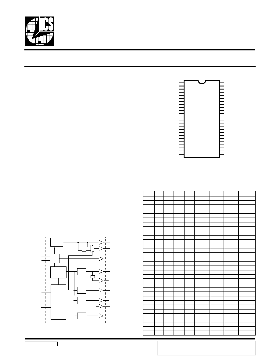
Pin Configuration
48-pin SSOP
*120K ohm pull-up to VDD on indicated inputs.
Recommended Application:
For Intel Camino Style Chipsets
Output Features:
·
3 - CPUs @ 2.5V, up to 180MHz.
·
1 - CPU/2 @ 2.5V.
·
3 - IOAPIC @ 2.5V, PCI or PCI/2
·
3 - 3V66MHz @ 3.3V.
·
11 - PCIs @ 3.3V
·
1 - 48MHz, @ 3.3V fixed
·
1 - 24/48MHz, @ 3.3V
Features:
·
Support power management: Power down Mode
from I
2
C programming.
·
Spread spectrum for EMI control
± 0.25% center spread).
·
Uses external 14.318MHz crystal
Key Specifications:
·
CPU Output Jitter: <250ps
·
IOAPIC Output Jitter: <500ps
·
48MHz, 3V66, PCI Output Jitter: <500ps)
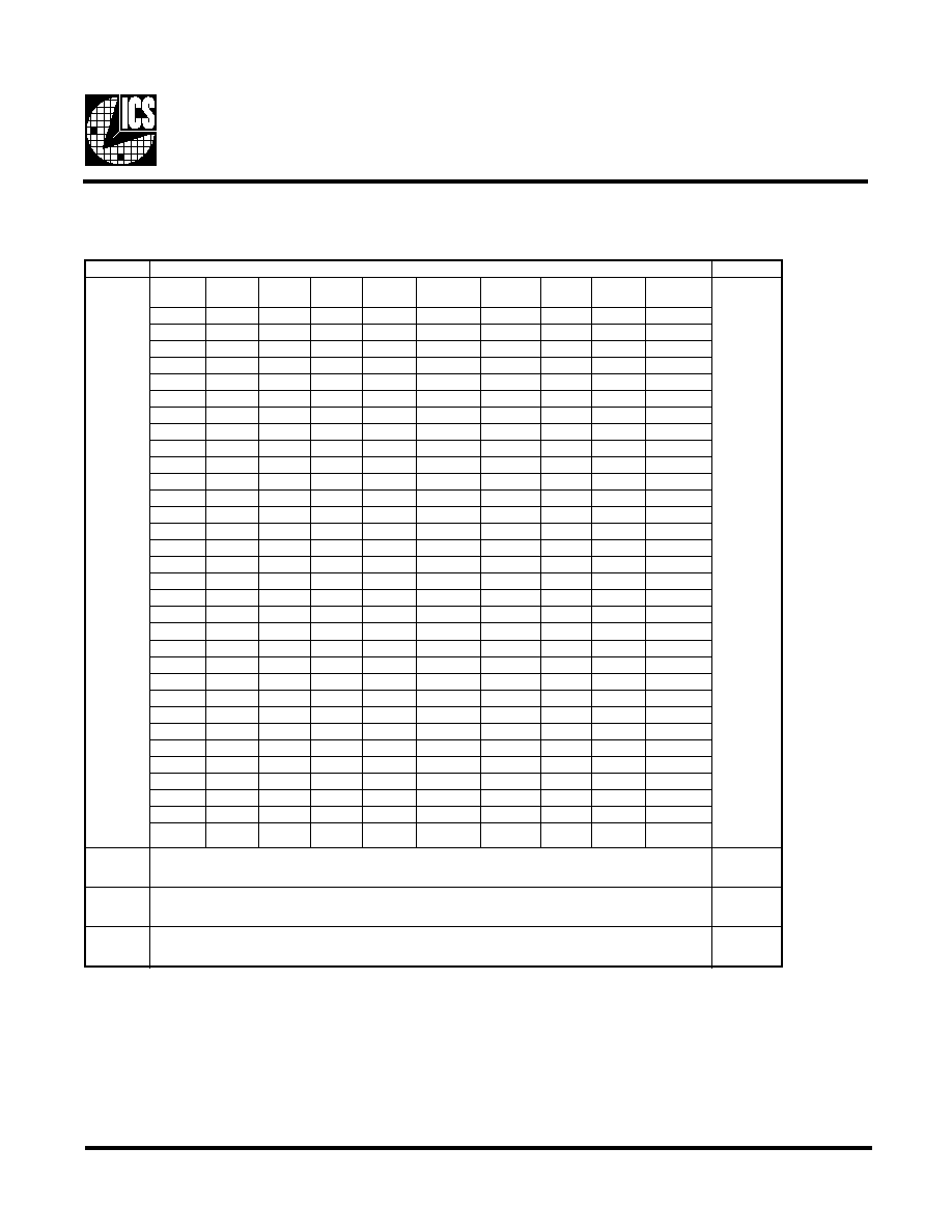
FREQ_APIC
SEL24_48#
PLL2
PLL1
Spread
Spectrum
48MHz
24_48MHz
CPUCLK (2:0)
IOAPIC (2:0)
PCICLK (9:0)
CPU/2
PCICLK_F
3V66 (2:0)
X1
X2
XTAL
OSC
CPU
DIVDER
IOAPIC
DIVDER
PCI
DIVDER
3V66
DIVDER
SDATA
SCLK
FS (4:0)
PD#
Control
Logic
Config.
Reg.
/ 2
/ 2
REF (1:0)
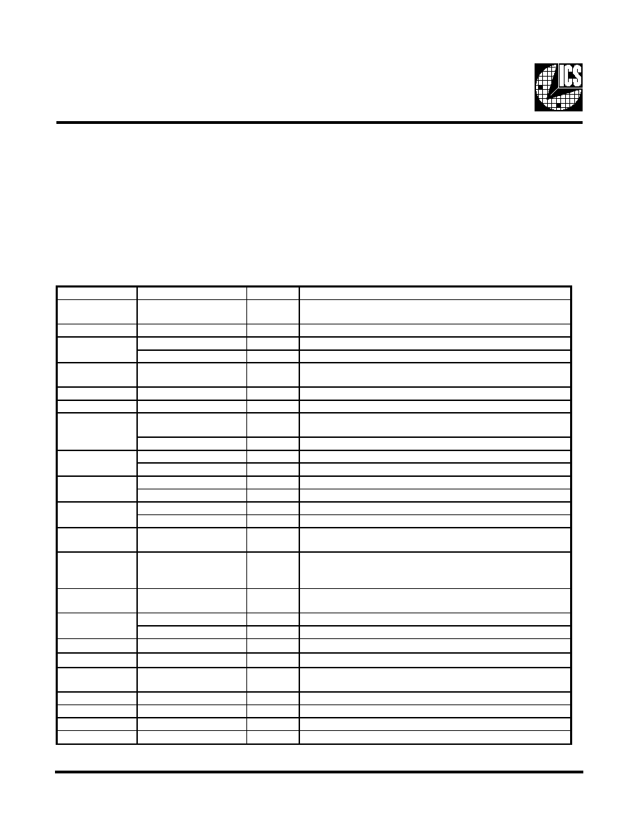
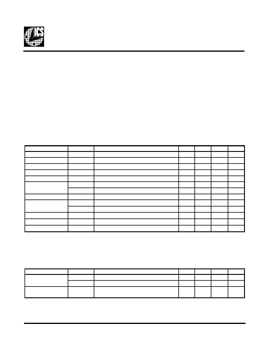
Functionality
FS4
FS3
FS2
FS1
FS0
CPU
PCI
3V 66
IOAPIC
0
0
0
0
0
103.00
34.33
68.67
17.17
0
0
0
0
1
105.00
35.00
70.00
17.50
0
0
0
1
0
100.45
33.483
66.967
16.742
0
0
0
1
1
100.90
33.63
67.27
16.82
0
0
1
0
0
107.10
35.700
71.400
17.850
0
0
1
0
1
109.00
36.33
72.67
18.17
0
0
1
1
0
112.00
37.34
74.67
18.67
0
0
1
1
1
114.00
28.50
57.00
14.25
0
1
0
0
0
116.00
29.00
58.00
14.50
0
1
0
0
1
118.00
29.50
59.00
14.75
0
1
0
1
0
133.30
33.33
66.65
16.66
0
1
0
1
1
120.00
30.00
60.00
15.00
0
1
1
0
0
122.00
30.50
61.00
15.25
0
1
1
0
1
125.00
31.25
62.50
15.63
0
1
1
1
0
128.21
32.05
64.105
16.026
0
1
1
1
1
130.00
32.50
65.00
16.25
1
0
0
0
0
132.00
33.00
66.00
16.50
1
0
0
0
1
133.90
33.48
66.95
16.74
1
0
0
1
0
138.00
34.50
69.00
17.25
1
0
0
1
1
142.00
35.50
71.00
17.75
1
0
1
0
0
146.00
36.50
73.00
18.25
1
0
1
0
1
150.00
37.50
75.00
18.75
1
0
1
1
0
153.00
38.25
76.50
19.13
1
0
1
1
1
156.00
39.00
78.00
19.50
1
1
0
0
0
159.00
39.75
79.50
19.88
1
1
0
0
1
162.00
40.50
81.00
20.25
1
1
0
1
0
165.00
41.25
82.50
20.63
1
1
0
1
1
168.00
42.00
84.00
21.00
1
1
1
0
0
171.00
42.75
85.50
21.38
1
1
1
0
1
174.00
43.50
87.00
21.75
1
1
1
1
0
177.00
44.25
88.50
22.13
1
1
1
1
1
180.00
45.00
90.00
22.50
ICS reserves the right to make changes in the device data identified in
this publication without further notice. ICS advises its customers to
obtain the latest version of all device data to verify that any
information being relied upon by the customer is current and accurate.
GND
REF0
*SEL24_48#/REF1
VDDREF
X1
X2
GND
*FS0/PCICLK_F
*FS1/PCICLK0
VDDPCI
*FS2/PCICLK1
*FS3/PCICLK2
GND
PCICLK3
PCICLK4
VDDPCI
PCICLK5
PCICLK6
GND
PCICLK7
PCICLK8
PCICLK9
VDDPCI
PD#
VDDL
IOAPIC0
IOAPIC1
GND
IOAPIC2
VDDL
CPU/2
GND
CPUCLK0
VDDL
CPUCLK1
CPUCLK2
GND
VDD66
3V66_0
3V66_1
3V66_2
GND66
SDATA
SCLK
VDD48
48MHz/FS4*
24_48MHz
GND48
ICS9248-134
1
2
3
4
5
6
7
8
9
10
11
12
13
14
15
16
17
18
19
20
21
22
23
24
48
47
46
45
44
43
42
41
40
39
38
37
36
35
34
33
32
31
30
29
28
27
26
25
2
ICS9248-134
Pin Descriptions
The ICS9248-134 is a main clock synthesizer chip for Pentium II based systems using Rambus Interface DRAMs. This chip
provides all the clocks required for such a system when used with a Direct Rambus Clock Generator(DRCG) chip such as the
ICS9212-01.
Spread Spectrum may be enabled by driving the SPREAD# pin active. Spread spectrum typically reduces system EMI by 8dB
to 10dB. This simplifies EMI qualification without resorting to board design iterations or costly shielding. The ICS9248-134
employs a proprietary closed loop design, which tightly controls the percentage of spreading over process and temperature
variations.
The CPU/2 clocks are inputs to the DRCG.
General Description
Pin number
Pin name
Type
Description
1, 7, 13, 19, 25, 31,
36, 41, 45
G ND
PWR
G round pins
2
REF0
OU T
14.318M Hz reference clock outputs at 3.3V
REF1
OU T
14.318M Hz reference clock outputs at 3.3V
SEL24_48
IN
Logic input to select 24 or 48M Hz for pin 26 output
4, 10, 16, 23,
28, 35
V DD
PWR
Power pins 3.3V
5
X 1
IN
X TAL_IN 14.318M Hz crystal input
6
X 2
OU T
X TAL_O UT Crystal output
PCICLK_F
OU T
Free running PCI clock at 3.3V . Synchronous to CPU clocks. Not
affected by the PCI_STOP# input.
FS0
IN
Logic - input for frequency selection
PCICLK0
OU T
PCI clock output at 3.3V . Synchronous to CPU clocks.
FS1
IN
Logic - input for frequency selection
PCICLK1
OU T
PCI clock output at 3.3V . Synchronous to CPU clocks.
FS2
IN
Logic - input for frequency selection
PCICLK2
OU T
PCI clock output at 3.3V . Synchronous to CPU clocks.
FS3
IN
Logic - input for frequency selection
14, 15, 17, 18, 20,
21, 22
PCICLK (9:3)
OU T
PCI clock outputs at 3.3V. Synchronous to CPU clocks.
24
PD #
IN
This asynchronous input powers down the chip when drive
active(Low). The internal PLLs are disabled and all the output clocks
are held at a Low state.
26
24_48M Hz
OU T
24 or 48M Hz output selectable by
SEL24_48# (0=48M Hz 1=24M Hz)
48M Hz
OU T
Fixed 48M Hz clock output. 3.3V
FS4
IN
Logic - input for frequency selection
29
SCLK
IN
Clock input of I
2
C input
30
SD ATA
I/O
D ata pin for I
2
C circuitry 5V tolerant
32, 33, 34
3V66 (2:0)
OU T
3.3V clock outputs. These outputs are stopped when CPU_STOP#
is driven active..
37, 38, 40
CPUCLK (2:0)
OU T
H ost bus clock output at 2.5V.
42
CPU/2
OU T
2.5V clock outputs at 1/2 CPU frequency.
39, 43, 48
V DDL
PWR
Power pins for the CPU, CPU/2 & IO APIC clocks. 2.5V
44, 46, 47
IOAPIC (2:0)
OU T
IOAPIC clocks at 2.5V. Synchronous with CPU CLKs.
27
12
3
8
9
11
3
ICS9248-134
Byte 0: Functionality and frequency select register (Default = 0)
Serial Configuration Command Bitmap
Note 1:
Default at power-up will be latched logic inputs to define frequency, as displayed by Bit 1.
t
i
B
n
o
i
t
p
i
r
c
s
e
D
D
W
P
t
i
B
4
:
7
,
2
2
t
i
B
4
S
F
7
t
i
B
3
S
F
6
t
i
B
2
S
F
5
t
i
B
1
S
F
4
t
i
B
0
S
F
U
P
C
2
/
U
P
C
I
C
P
6
6
V
3
C
I
P
A
O
I
d
e
v
r
e
s
e
R
1
e
t
o
N
0
0
0
0
0
0
0
.
3
0
1
0
5
.
1
5
3
3
.
4
3
7
6
.
8
6
7
1
.
7
1
0
0
0
0
1
0
0
.
5
0
1
0
5
.
2
5
0
0
.
5
3
0
0
.
0
7
0
5
.
7
1
0
0
0
1
0
5
4
.
0
0
1
5
2
2
.
0
5
3
8
4
.
3
3
7
6
9
.
6
6
2
4
7
.
6
1
0
0
0
1
1
0
9
.
0
0
1
5
4
.
0
5
3
6
.
3
3
7
2
.
7
6
2
8
.
6
1
0
0
1
0
0
0
1
.
7
0
1
0
5
5
.
3
5
0
0
7
.
5
3
0
0
4
.
1
7
0
5
8
.
7
1
0
0
1
0
1
0
0
.
9
0
1
0
5
.
4
5
3
3
.
6
3
7
6
.
2
7
7
1
.
8
1
0
0
1
1
0
0
0
.
2
1
1
0
0
.
6
5
4
3
.
7
3
7
6
.
4
7
7
6
.
8
1
0
0
1
1
1
0
0
.
4
1
1
0
0
.
7
5
0
5
.
8
2
0
0
.
7
5
5
2
.
4
1
0
1
0
0
0
0
0
.
6
1
1
0
0
.
8
5
0
0
.
9
2
0
0
.
8
5
0
5
.
4
1
0
1
0
0
1
0
0
.
8
1
1
0
0
.
9
5
0
5
.
9
2
0
0
.
9
5
5
7
.
4
1
0
1
0
1
0
0
3
.
3
3
1
5
6
.
6
6
3
3
.
3
3
5
6
.
6
6
6
6
.
6
1
0
1
0
1
1
0
0
.
0
2
1
0
0
.
0
6
0
0
.
0
3
0
0
.
0
6
0
0
.
5
1
0
1
1
0
0
0
0
.
2
2
1
0
0
.
1
6
0
5
.
0
3
0
0
.
1
6
5
2
.
5
1
0
1
1
0
1
0
0
.
5
2
1
0
5
.
2
6
5
2
.
1
3
0
5
.
2
6
3
6
.
5
1
0
1
1
1
0
1
2
.
8
2
1
5
0
1
.
4
6
5
0
.
2
3
5
0
1
.
4
6
6
2
0
.
6
1
0
1
1
1
1
0
0
.
0
3
1
0
0
.
5
6
0
5
.
2
3
0
0
.
5
6
5
2
.
6
1
1
0
0
0
0
0
0
.
2
3
1
0
0
.
6
6
0
0
.
3
3
0
0
.
6
6
0
5
.
6
1
1
0
0
0
1
0
9
.
3
3
1
5
9
.
6
6
8
4
.
3
3
5
9
.
6
6
4
7
.
6
1
1
0
0
1
0
0
0
.
8
3
1
0
0
.
9
6
0
5
.
4
3
0
0
.
9
6
5
2
.
7
1
1
0
0
1
1
0
0
.
2
4
1
0
0
.
1
7
0
5
.
5
3
0
0
.
1
7
5
7
.
7
1
1
0
1
0
0
0
0
.
6
4
1
0
0
.
3
7
0
5
.
6
3
0
0
.
3
7
5
2
.
8
1
1
0
1
0
1
0
0
.
0
5
1
0
0
.
5
7
0
5
.
7
3
0
0
.
5
7
5
7
.
8
1
1
0
1
1
0
0
0
.
3
5
1
0
5
.
6
7
5
2
.
8
3
0
5
.
6
7
3
1
.
9
1
1
0
1
1
1
0
0
.
6
5
1
0
0
.
8
7
0
0
.
9
3
0
0
.
8
7
0
5
.
9
1
1
1
0
0
0
0
0
.
9
5
1
0
5
.
9
7
5
7
.
9
3
0
5
.
9
7
8
8
.
9
1
1
1
0
0
1
0
0
.
2
6
1
0
0
.
1
8
0
5
.
0
4
0
0
.
1
8
5
2
.
0
2
1
1
0
1
0
0
0
.
5
6
1
0
5
.
2
8
5
2
.
1
4
0
5
.
2
8
3
6
.
0
2
1
1
0
1
1
0
0
.
8
6
1
0
0
.
4
8
0
0
.
2
4
0
0
.
4
8
0
0
.
1
2
1
1
1
0
0
0
0
.
1
7
1
0
5
.
5
8
5
7
.
2
4
0
5
.
5
8
8
3
.
1
2
1
1
1
0
1
0
0
.
4
7
1
0
0
.
7
8
0
5
.
3
4
0
0
.
7
8
5
7
.
1
2
1
1
1
1
0
0
0
.
7
7
1
0
5
.
8
8
5
2
.
4
4
0
5
.
8
8
3
1
.
2
2
1
1
1
1
1
0
0
.
0
8
1
0
0
.
0
9
0
0
.
5
4
0
0
.
0
9
0
5
.
2
2
3
t
i
B
s
t
u
p
n
i
d
e
h
c
t
a
l
,
t
c
e
l
e
s
e
r
a
w
d
r
a
h
y
b
d
e
t
c
e
l
e
s
s
i
y
c
n
e
u
q
e
r
F
-
0
4
:
7
,
2
t
i
B
y
b
d
e
t
c
e
l
e
s
s
i
y
c
n
e
u
q
e
r
F
-
1
0
1
t
i
B
d
e
l
b
a
s
i
d
m
u
r
t
c
e
p
S
d
a
e
r
p
S
-
0
d
e
l
b
a
n
e
m
u
r
t
c
e
p
s
d
a
e
r
p
S
-
1
1
0
t
i
B
g
n
i
n
n
u
R
-
0
s
t
u
p
t
u
o
l
l
a
e
t
a
t
s
i
r
T
-
1
0
4
ICS9248-134
Byte 1: CPU, Active/Inactive Register
(1 = enable, 0 = disable)
Byte 2: PCI Active/Inactive Register
(1 = enable, 0 = disable)
Byte 3: 3V66 Active/Inactive Register
(1 = enable, 0 = disable)
Notes:
1. Inactive means outputs are held LOW and are disabled
from switching.
Notes:
1. Inactive means outputs are held LOW and are disabled
from switching.
Notes:
1. Inactive means outputs are held LOW and are disabled
from switching.
Byte 4: PCI Active/Inactive Register
(1 = enable, 0 = disable)
Notes:
1. Inactive means outputs are held LOW and are disabled
from switching.
t
i
B
#
n
i
P
D
W
P
n
o
i
t
p
i
r
c
s
e
D
7
t
i
B
0
4
1
0
K
L
C
U
P
C
6
t
i
B
8
3
1
1
K
L
C
U
P
C
5
t
i
B
7
3
1
2
K
L
C
U
P
C
4
t
i
B
2
4
1
2
/
U
P
C
3
t
i
B
7
4
1
0
C
I
P
A
O
I
2
t
i
B
6
4
1
1
C
I
P
A
O
I
1
t
i
B
4
4
1
2
C
I
P
A
O
I
0
t
i
B
-
X
)
d
e
v
r
e
s
e
R
(
t
i
B
#
n
i
P
D
W
P
n
o
i
t
p
i
r
c
s
e
D
7
t
i
B
8
1
1
7
K
L
C
I
C
P
6
t
i
B
7
1
1
6
K
L
C
I
C
P
5
t
i
B
5
1
1
5
K
L
C
I
C
P
4
t
i
B
4
1
1
4
K
L
C
I
C
P
3
t
i
B
2
1
1
3
K
L
C
I
C
P
2
t
i
B
1
1
1
2
K
L
C
I
C
P
1
t
i
B
9
1
1
K
L
C
I
C
P
0
t
i
B
8
1
F
_
K
L
C
I
C
P
t
i
B
#
n
i
P
D
W
P
n
o
i
t
p
i
r
c
s
e
D
7
t
i
B
4
3
1
0
_
6
6
V
3
6
t
i
B
3
3
1
1
_
6
6
V
3
5
t
i
B
2
3
1
2
_
6
6
V
3
4
t
i
B
-
X
#
1
S
F
3
t
i
B
3
1
1
F
E
R
2
t
i
B
2
1
0
F
E
R
1
t
i
B
-
X
#
3
S
F
0
t
i
B
-
X
#
2
S
F
t
i
B
#
n
i
P
D
W
P
n
o
i
t
p
i
r
c
s
e
D
7
t
i
B
6
2
1
z
H
M
8
4
_
4
2
6
t
i
B
7
2
1
z
H
M
8
4
5
t
i
B
-
X
#
0
S
F
4
t
i
B
-
1
)
d
e
v
r
e
s
e
R
(
3
t
i
B
2
2
1
0
1
K
L
C
I
C
P
2
t
i
B
1
2
1
9
K
L
C
I
C
P
1
t
i
B
0
2
1
8
K
L
C
I
C
P
0
t
i
B
-
X
#
4
S
F
Byte 5: Active/Inactive Register
(1= enable, 0 = disable)
t
i
B
#
n
i
P
D
W
P
n
o
i
t
p
i
r
c
s
e
D
7
t
i
B
-
0
)
e
t
o
N
(
d
e
v
r
e
s
e
R
6
t
i
B
-
0
)
e
t
o
N
(
d
e
v
r
e
s
e
R
5
t
i
B
-
0
)
e
t
o
N
(
d
e
v
r
e
s
e
R
4
t
i
B
-
0
)
e
t
o
N
(
d
e
v
r
e
s
e
R
3
t
i
B
-
0
)
e
t
o
N
(
d
e
v
r
e
s
e
R
2
t
i
B
-
1
)
e
t
o
N
(
d
e
v
r
e
s
e
R
1
t
i
B
-
1
)
e
t
o
N
(
d
e
v
r
e
s
e
R
0
t
i
B
-
0
)
e
t
o
N
(
d
e
v
r
e
s
e
R
Byte6: Active/Inactive Register
(1= enable, 0 = disable)
Note: Don't write into this register, writing into this register
can cause malfunction
t
i
B
#
n
i
P
D
W
P
n
o
i
t
p
i
r
c
s
e
D
7
t
i
B
-
1
)
e
t
o
N
(
d
e
v
r
e
s
e
R
6
t
i
B
-
1
)
e
t
o
N
(
d
e
v
r
e
s
e
R
5
t
i
B
-
1
)
e
t
o
N
(
d
e
v
r
e
s
e
R
4
t
i
B
-
1
)
e
t
o
N
(
d
e
v
r
e
s
e
R
3
t
i
B
-
1
)
e
t
o
N
(
d
e
v
r
e
s
e
R
2
t
i
B
-
1
)
e
t
o
N
(
d
e
v
r
e
s
e
R
1
t
i
B
-
1
)
e
t
o
N
(
d
e
v
r
e
s
e
R
0
t
i
B
-
1
)
e
t
o
N
(
d
e
v
r
e
s
e
R
Notes:
1. Inactive means outputs are held LOW and are disabled
from switching.
5
ICS9248-134
Absolute Maximum Ratings
Supply Voltage . . . . . . . . . . . . . . . . . . . . . . . . . . 5.5 V
Logic Inputs . . . . . . . . . . . . . . . . . . . . . . . . . . . . GND 0.5 V to V
DD
+0.5 V
Ambient Operating Temperature . . . . . . . . . . . . 0°C to +70°C
Storage Temperature . . . . . . . . . . . . . . . . . . . . . . 65°C to +150°C
Case Temperature . . . . . . . . . . . . . . . . . . . . . . . . 115°C
Stresses above those listed under Absolute Maximum Ratings may cause permanent damage to the device. These ratings are
stress specifications only and functional operation of the device at these or any other conditions above those listed in the
operational sections of the specifications is not implied. Exposure to absolute maximum rating conditions for extended
periods may affect product reliability.
Electrical Characteristics - Input/Supply/Common Output Parameters
T
A
= 0 - 70º C; V
DD
= 3.3 V +/-5%; V
DDL
= 2.5 V +/-5% (unless otherwise stated)
PARAMETER
SYMBOL
CONDITIONS
MIN
TYP
MAX
UNITS
Input High Voltage
V
IH
2
V
DD
+0.3
V
Input Low Voltage
V
IL
V
SS
-0.3
0.8
V
Input High Current
I
IH
V
IN
= V
DD
0.1
5
µ
A
Input Low Current
I
IL1
V
IN
= 0 V; Inputs with no pull-up resistors
-5
2.0
µ
A
Input Low Current
I
IL2
V
IN
= 0 V; Inputs with pull-up resistors
-200
-100
µ
A
Operating
I
DD3.3OP100
C
L
= 0 pF; Select @ 100 MHz
71
160
mA
Supply Current
I
DD3.3OP133
C
L
= 0 pF; Select @ 133 MHz
76
160
mA
Input frequency
F
i
V
DD
= 3.3 V;
11
14.318
16
MHz
Input Capacitance
1
C
IN
Logic Inputs
5
pF
C
INX
X1 & X2 pins
27
36
45
pF
Transition Time
1
T
trans
To 1st crossing of target Freq.
3
ms
Settling Time
1
T
s
From 1st crossing to 1% target Freq.
5
ms
Clk Stabilization
1
T
STAB
From V
DD
= 3.3 V to 1% target Freq.
3
ms
1
Guaranteed by design, not 100% tested in production.
Electrical Characteristics - Input/Supply/Common Output Parameters
T
A
= 0 - 70º C; V
DD
= 3.3 V +/-5%; V
DDL
= 2.5 V +/-5% (unless otherwise stated)
PARAMETER
SYMBOL
CONDITIONS
MIN
TYP
MAX
UNITS
Operating
I
DD2.5OP100
C
L
= 0 pF; Select @ 100 MHz
15
75
mA
Supply Current
I
DD2.5OP133
C
L
= 0 pF; Select @ 133 MHz
18
90
mA
Power Down
Supply Current
1
Guaranteed by design, not 100% tested in production.
µ
A
I
DD2.5PD
C
L
= 0 pF; PWRDWN# = 0
272
400