Integrated
Circuit
Systems, Inc.
ICS9248-150
Third party brands and names are the property of their respective owners.
9248-150 Rev B 06/12/01
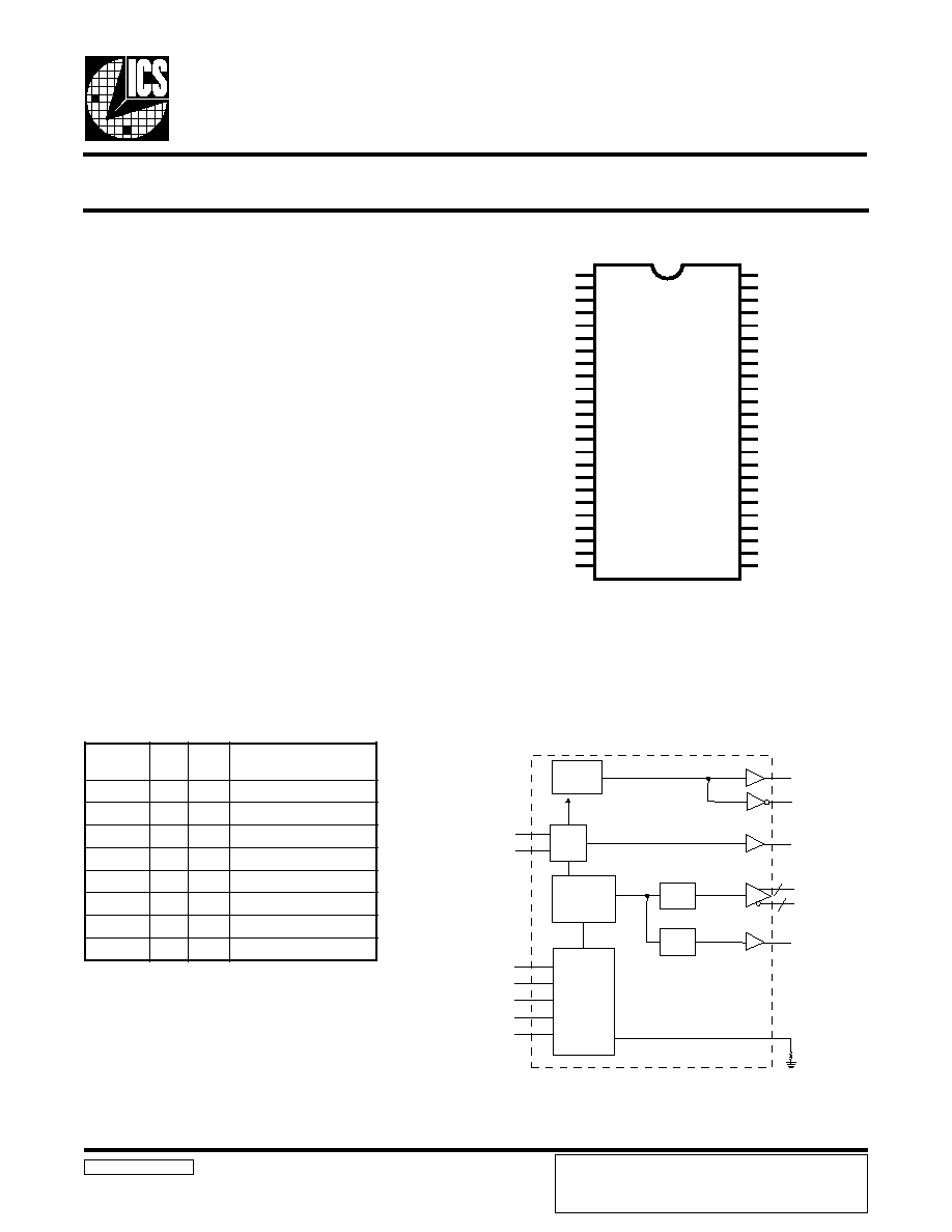
Pin Configuration
48-Pin SSOP and TSSOP
Recommended Application:
ServerWorks Grand Champion Systems.
Output Features:
·
8 - Differential CPU Clock Pairs @ 3.3V
·
1 - 3V 33MHz PCI clocks
·
1 - 48MHz clock
·
1 - Inverted 48MHz clock
·
1 - 14.318 reference output
Features:
·
Up to 200MHz frequency support
·
Support power management: Power Down Mode
·
Supports Spread Spectrum modulation: 0 to -0.5% down
spread.
·
Uses external 14.318MHz crystal
·
Select logic for Differential Swing Control, Test mode,
Tristate, Power down, Spread Spectrum.
·
External resistor for current reference
·
FS pins for frequency select
Key Specifications:
·
PCI Output jitter <500ps
·
CPU Output jitter <200ps
·
48MHz Output jitter <350ps
·
REF Output jitter < 1000ps
Frequency Generator for Multi - Processor Servers
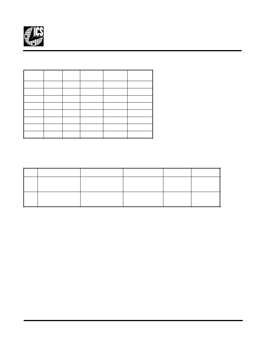
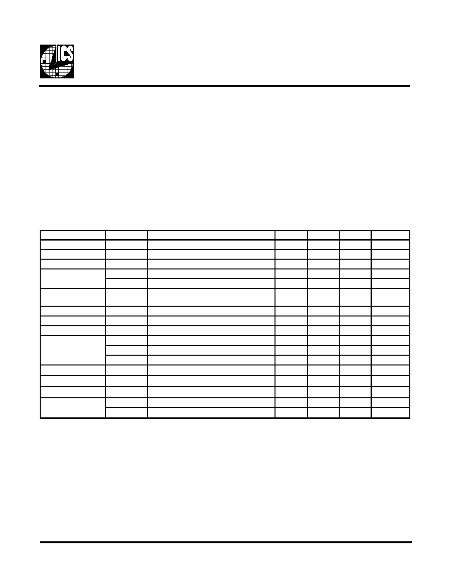
Functionality
/
3
3
1
L
E
S
0
0
1
0
S
F
1
S
F
n
o
i
t
c
n
u
F
0
0
0
z
H
M
0
0
1
e
v
i
t
c
A
0
0
1
e
d
o
M
t
s
e
T
z
H
M
0
0
1
0
1
0
e
d
o
M
t
s
e
T
z
H
M
0
0
1
0
1
1
s
t
u
p
t
u
o
l
l
a
e
t
a
t
s
i
r
T
1
0
0
z
H
M
3
3
1
e
v
i
t
c
A
1
0
1
e
d
o
M
t
s
e
T
z
H
M
3
3
1
1
1
0
z
H
M
0
0
2
e
v
i
t
c
A
1
1
1
d
e
v
r
e
s
e
R
Block Diagram
PCICLK
VDD48
FS0/48MHz
FS1/48MHz#
GND48
VDDCPU
CPUCLKT0
CPUCLKC0
GNDCPU
CPUCLKT1
CPUCLKC1
VDDCPU
CPUCLKT2
CPUCLKC2
GNDCPU
CPUCLKT3
CPUCLKC3
VDDCPU
REF
SPREAD#
GNDREF
X1
X2
VDDREF
SEL100/133
GNDPCI
VDDA
GNDA
PD#
VDDCPU
CPUCLKT4
CPUCLKC4
GNDCPU
CPUCLKT5
CPUCLKC5
VDDCPU
CPUCLKT6
CPUCLKC6
GNDCPU
CPUCLKT7
CPUCLKC7
VDDCPU
MULTSEL0
MULTSEL1
GND
GNDI REF
I REF
VDDI REF
ICS9248-150
1
2
3
4
5
6
7
8
9
10
11
12
13
14
15
16
17
18
19
20
21
22
23
24
48
47
46
45
44
43
42
41
40
39
38
37
36
35
34
33
32
31
30
29
28
27
26
25
I REF
PLL2
PLL1
Spread
Spectrum
48MHz
PCICLK
48MHz#
X1
X2
XTAL
OSC
CPU
DIVDER
PCI
DIVDER
PD#
SPREAD#
MULTSEL(1:0)
SEL100/133
FS(1:0)
Control
Logic
Config.
Reg.
REF
8
8
CPUCLKT (7:0)
CPUCLKC (7:0)
ICS reserves the right to make changes in the device data
identified in this publication without further notice. ICS advises
its customers to obtain the latest version of all device data to
verify that any information being relied upon by the customer is
Analog Power Groups
VDD48, GND48 = 48MHz, PLL2
VDDA=VDD (core supply voltage 3.3V)
GNDA=Ground for core supply
Digital Power Group
VDDREF, GNDREF = REF, Xtal
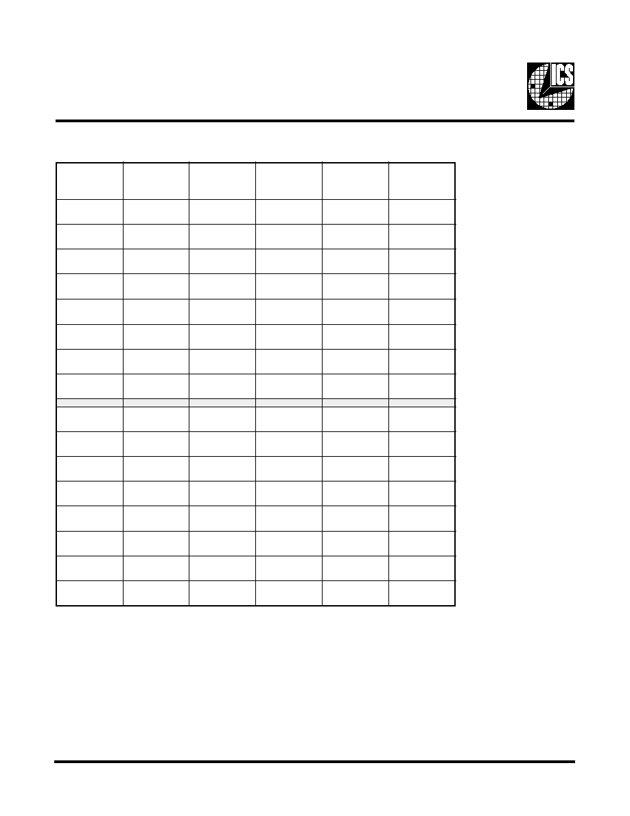
2
ICS9248-150
Third party brands and names are the property of their respective owners.
General Description
Pin Configuration
The ICS9248-150 is a main clock for ServerWorks Grand Champion Systems.
Spread spectrum typically reduces system EMI by 8dB to 10dB. This simplifies EMI qualification without resorting to
board design iterations or costly shielding. The ICS9248-150 employs a proprietary closed loop design, which tightly
controls the percentage of spreading over process and temperature variations.
R
E
B
M
U
N
N
I
P
E
M
A
N
N
I
P
E
P
Y
T
N
O
I
T
P
I
R
C
S
E
D
1
K
L
C
I
C
P
T
U
O
t
u
p
t
u
o
k
c
o
l
c
I
C
P
,
1
3
,
4
2
,
8
1
,
2
1
,
6
,
2
,
3
4
,
7
3
D
D
V
R
W
P
y
l
p
p
u
s
r
e
w
o
p
V
3
.
3
3
0
S
F
N
I
n
i
p
t
c
e
l
e
s
y
c
n
e
u
q
e
r
F
z
H
M
8
4
T
U
O
t
u
p
t
u
o
k
c
o
l
c
z
H
M
8
4
4
1
S
F
N
I
n
i
p
t
c
e
l
e
s
y
c
n
e
u
q
e
r
F
#
z
H
M
8
4
T
U
O
t
u
p
t
u
o
k
c
o
l
c
z
H
M
8
4
d
e
t
r
e
v
n
I
,
4
3
,
8
2
,
1
2
,
5
1
,
9
,
5
7
4
,
0
4
D
N
G
R
W
P
y
l
p
p
u
s
V
3
.
3
r
o
f
s
n
i
p
d
n
u
o
r
G
,
6
1
,
2
4
,
9
3
,
6
3
,
3
3
7
,
0
1
,
3
1
)
0
:
7
(
T
K
L
C
U
P
C
T
U
O
t
n
e
r
r
u
c
e
r
a
e
s
e
h
T
.
s
t
u
p
t
u
o
U
P
C
r
i
a
p
l
a
i
t
n
e
r
e
f
f
i
d
f
o
s
k
c
o
l
c
"
e
u
r
T
"
.
s
a
i
b
e
g
a
t
l
o
v
r
o
f
d
e
r
i
u
q
e
r
e
r
a
s
r
o
t
s
i
s
e
r
l
a
n
r
e
t
x
e
d
n
a
s
t
u
p
t
u
o
,
7
1
,
1
4
,
8
3
,
5
3
,
2
3
8
,
1
1
,
4
1
)
0
:
7
(
C
K
L
C
U
P
C
T
U
O
e
r
a
e
s
e
h
T
.
s
t
u
p
t
u
o
U
P
C
r
i
a
p
l
a
i
t
n
e
r
e
f
f
i
d
f
o
s
k
c
o
l
c
"
y
r
o
t
n
e
m
e
l
p
m
o
C
"
.
s
a
i
b
e
g
a
t
l
o
v
r
o
f
d
e
r
i
u
q
e
r
e
r
a
s
r
o
t
s
i
s
e
r
l
a
n
r
e
t
x
e
d
n
a
s
t
u
p
t
u
o
t
n
e
r
r
u
c
9
1
F
E
R
T
U
O
z
H
M
8
1
3
.
4
1
t
u
p
t
u
o
e
c
n
e
r
e
f
e
R
0
2
#
D
A
E
R
P
S
N
I
t
s
o
h
l
a
i
t
n
e
r
e
f
f
i
D
e
h
t
n
o
y
t
i
l
a
n
o
i
t
c
n
u
f
m
u
r
t
c
e
p
S
d
a
e
r
p
S
s
e
k
o
v
n
I
w
o
L
e
v
i
t
c
A
,
s
k
c
o
l
c
2
2
1
X
t
u
p
n
I
l
a
t
s
y
r
C
2
X
t
u
p
n
i
l
a
t
s
y
r
C
z
H
M
8
1
3
.
4
1
3
2
2
X
t
u
p
t
u
O
l
a
t
s
y
r
C
1
X
t
u
p
t
u
o
l
a
t
s
y
r
C
z
H
M
8
1
3
.
4
1
6
4
,
5
2
F
E
R
I
D
D
V
,
A
D
D
V
R
W
P
V
3
.
3
y
l
p
p
u
s
r
e
w
o
p
g
o
l
a
n
A
6
2
F
E
R
I
T
U
O
.
s
r
i
a
p
K
L
C
U
P
C
e
h
t
r
o
f
t
n
e
r
r
u
c
e
c
n
e
r
e
f
e
r
e
h
t
s
e
h
s
i
l
b
a
t
s
e
n
i
p
s
i
h
T
o
t
r
e
d
r
o
n
i
d
n
u
o
r
g
o
t
d
e
i
t
r
o
t
s
i
s
e
r
n
o
i
s
i
c
e
r
p
d
e
x
i
f
a
s
e
k
a
t
n
i
p
s
i
h
T
.
t
n
e
r
r
u
c
d
e
r
i
u
q
e
r
e
h
t
h
s
i
l
b
a
t
s
e
0
3
,
9
2
)
0
:
1
(
L
E
S
T
L
U
M
N
I
s
t
u
p
n
i
t
c
e
l
e
s
g
n
i
w
s
U
P
C
4
4
#
D
P
N
I
.
w
o
L
e
v
i
t
c
A
.
e
d
o
m
n
w
o
d
-
r
e
w
o
p
s
e
k
o
v
n
I
5
4
,
7
2
F
E
R
I
D
N
G
A
D
N
G
R
W
P
y
l
p
p
u
s
V
3
.
3
r
o
f
s
n
i
p
d
n
u
o
r
G
g
o
l
a
n
A
8
4
3
3
1
/
0
0
1
L
E
S
N
I
z
H
M
3
3
1
=
h
g
i
H
,
z
H
M
0
0
1
=
w
o
L
.
t
c
e
l
e
S
y
c
n
e
u
q
e
r
F
U
P
C
5
ICS9248-150
Third party brands and names are the property of their respective owners.
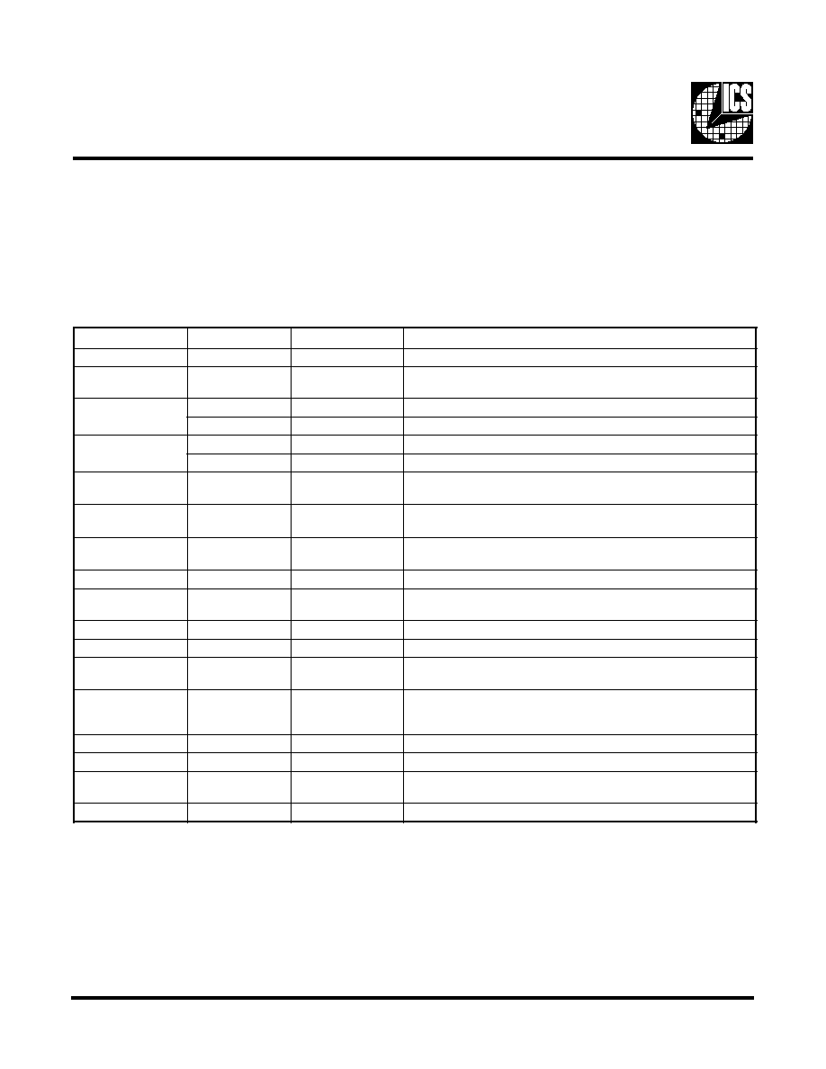
Absolute Maximum Ratings
Supply Voltage . . . . . . . . . . . . . . . . . . . . . . . . . . . . 5.5 V
Logic Inputs . . . . . . . . . . . . . . . . . . . . . . . . . . . . . . GND 0.5 V to V
DD
+0.5 V
Ambient Operating Temperature . . . . . . . . . . . . . 0°C to +70°C
Case Temperature . . . . . . . . . . . . . . . . . . . . . . . . . . 115°C
Storage Temperature . . . . . . . . . . . . . . . . . . . . . . . 65°C to +150°C
Stresses above those listed under Absolute Maximum Ratings may cause permanent damage to the device. These ratings are
stress specifications only and functional operation of the device at these or any other conditions above those listed in the
operational sections of the specifications is not implied. Exposure to absolute maximum rating conditions for extended periods
may affect product reliability.
Electrical Characteristics - Input/Supply/Common Output Parameters
T
A
= 0 - 70C; Supply Voltage V
DD
= 3.3 V +/-5%
PARAMETER
SYMBOL
CONDITIONS
MIN
TYP
MAX
UNITS
Input High Voltage
V
IH
2
V
DD
+0.3
V
Input Low Voltage
V
IL
V
SS
-0.3
0.8
V
Input High Current
I
IH
V
IN
= V
DD
-5
5
µ
A
I
IL1
V
IN
= 0 V; Inputs with no pull-up resistors
-5
µ
A
I
IL2
V
IN
= 0 V; Inputs with pull-up resistors
-200
Operating Supply
Current
I
DD3.3OP
C
L
= 0 pF; Select @ 100 MHz
181
250
mA
Powerdown Current
I
DD3.3PD
C
L
= 0 pF; Input address to VDD or GND
52
60
mA
Input Frequency
F
i
V
DD
= 3.3 V
14.318
MHz
Pin Inductance
L
pin
7
nH
C
IN
Logic Inputs
5
pF
C
OUT
Output pin capacitance
6
pF
C
INX
X1 & X2 pins
27
45
pF
Transition time
1
T
trans
To 1st crossing of target frequency
3
ms
Settling time
1
T
s
From 1st crossing to 1% target frequency
3
ms
Clk Stabilization
1
T
STAB
From V
DD
= 3.3 V to 1% target frequency
3
ms
t
PZH
,t
PZL
Output enable delay (all outputs)
1
10
ns
t
PHZ
,t
PLZ
Output disable delay (all outputs)
1
10
ns
1
Guaranteed by design, not 100% tested in production.
Delay
1
Input Capacitance
1
Input Low Current