8752CY
www.icst.com/products/hiperclocks.html
REV. A AUGUST 19, 2002
1
Integrated
Circuit
Systems, Inc.
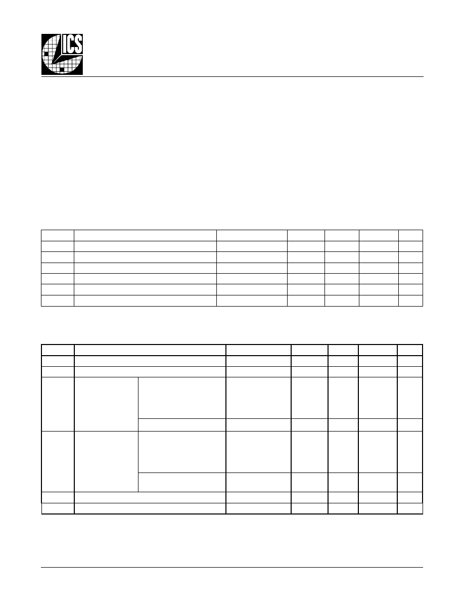
ICS8752
L
OW
S
KEW
, 1-
TO
-8
LVCMOS C
LOCK
M
ULTIPLIER
/Z
ERO
D
ELAY
B
UFFER
B
LOCK
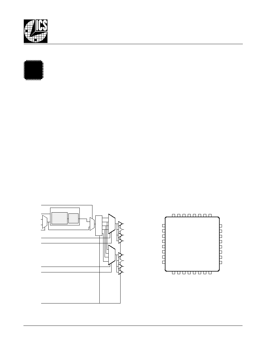
D
IAGRAM
P
IN
A
SSIGNMENT
32 31 30 29 28 27 26 25
9 10 11 12 13 14 15 16
1
2
3
4
5
6
7
8
24
23
22
21
20
19
18
17
GND
QB1
QB0
V
DDO
V
DDO
QA3
QA2
GND
DIV_SELB0
DIV_SELB1
DIV_SELA0
DIV_SELA1
MR/nOE
CLK0
GND
FB_IN
V
DDO
QA1
QA0
GND
CLK1
V
DD
V
DDA
CLK_SEL
V
DDO
QB2
QB3
GND
GND
nc
PLL_SEL
V
DD
ICS8752
32-Lead LQFP
7mm x 7mm x 1.4mm package body
Y package
Top View
÷2
÷4
÷6
÷8
÷12
PLL
PHASE
DETECTOR
PLL_SEL
FB_IN
CLK0
CLK1
CLK_SEL
DIV_SELA1
DIV_SELA0
DIV_SELB1
DIV_SELB0
MR/nOE
QA0
QA1
QA2
QA3
QB0
QB1
QB2
QB3
0
1
1
0
00
01
10
11
00
01
10
11
VCO
G
ENERAL
D
ESCRIPTION
The ICS8752 is a low voltage, low skew
LVCMOS clock generator and a member of
the HiPerClockSTM family of High Performance
Clock Solutions from ICS. With output fre-
quencies up to 240MHz, the ICS8752 is targeted
for high performance clock applications. Along with a fully in-
tegrated PLL, the ICS8752 contains frequency configurable
outputs and an external feedback input for regenerating clocks
with "zero delay".
Dual clock inputs, CLK0 and CLK1, support redundant clock
applications. The CLK_SEL input determines which reference
clock is used. The output divider values of Bank A and B are
controlled by the DIV_SELA0:1, and DIV_SELB0:1, respectively.
For test and system debug purposes, the PLL_SEL input
allows the PLL to be bypassed. When HIGH, the MR/nOE
input resets the internal dividers and forces the outputs to
the high impedance state.
The low impedance LVCMOS outputs of the ICS8752 are
designed to drive terminated transmission lines. The effec-
tive fanout of each output can be doubled by utilizing the
ability of each output to drive two series terminated trans-
mission lines.
F
EATURES
·
Fully integrated PLL
·
8 LVCMOS outputs, 7
typical output impedance
·
Selectable LVCMOS CLK0 or CLK1 inputs for
redundant clock applications
·
Input/Output frequency range: 18.33MHz to 240MHz
at V
CC
= 3.3V ± 5%
·
VCO range: 220MHz to 480MHz
·
External feedback for "zero delay" clock regeneration
·
Cycle-to-cycle jitter: 75ps (maximum),
(all outputs are the same frequency)
·
Output skew: 100ps (maximum)
·
Bank skew: 55ps (maximum)
·
3.3V or 2.5V supply voltage
·
0°C to 70°C ambient operating temperature
·
Industrial temperature information available upon request
·
Functionally compatible with MPC952 in some applications
HiPerClockSTM
,&6
8752CY
www.icst.com/products/hiperclocks.html
REV. A AUGUST 19, 2002
5
Integrated
Circuit
Systems, Inc.
ICS8752
L
OW
S
KEW
, 1-
TO
-8
LVCMOS C
LOCK
M
ULTIPLIER
/Z
ERO
D
ELAY
B
UFFER
T
ABLE
5B. LVCMOS/LVTTL DC C
HARACTERISTICS
,
V
DD
= V
DDA
= V
DDO
= 3.3V±5%, T
A
= 0°C
TO
70°C
T
ABLE
5A. P
OWER
S
UPPLY
DC C
HARACTERISTICS
,
V
DD
= V
DDA
= V
DDO
= 3.3V±5%, T
A
= 0°C
TO
70°C
A
BSOLUTE
M
AXIMUM
R
ATINGS
Supply Voltage, V
DDx
4.6V
Inputs, V
I
-0.5V to V
DD
+ 0.5V
Outputs, V
O
-0.5V to V
DDO
+ 0.5V
Package Thermal Impedance,
JA
47.9°C/W (0 lfpm)
Storage Temperature, T
STG
-65°C to 150°C
Stresses beyond those listed under Absolute Maximum Ratings may cause permanent damage to the device. These ratings
are stress specifications only. Functional operation of product at these conditions or any conditions beyond those listed in the
DC Characteristics or AC Characteristics is not implied. Exposure to absolute maximum rating conditions for extended peri-
ods may affect product reliability.
l
o
b
m
y
S
r
e
t
e
m
a
r
a
P
s
n
o
i
t
i
d
n
o
C
t
s
e
T
m
u
m
i
n
i
M
l
a
c
i
p
y
T
m
u
m
i
x
a
M
s
t
i
n
U
V
D
D
e
g
a
t
l
o
V
y
l
p
p
u
S
e
v
i
t
i
s
o
P
5
3
1
.
3
3
.
3
5
6
4
.
3
V
V
A
D
D
e
g
a
t
l
o
V
y
l
p
p
u
S
g
o
l
a
n
A
5
3
1
.
3
3
.
3
5
6
4
.
3
V
V
O
D
D
e
g
a
t
l
o
V
y
l
p
p
u
S
t
u
p
t
u
O
5
3
1
.
3
3
.
3
5
6
4
.
3
V
I
D
D
t
n
e
r
r
u
C
y
l
p
p
u
S
e
v
i
t
i
s
o
P
5
0
1
A
m
I
A
D
D
t
n
e
r
r
u
C
y
l
p
p
u
S
g
o
l
a
n
A
5
1
A
m
I
O
D
D
t
n
e
r
r
u
C
y
l
p
p
u
S
t
u
p
t
u
O
0
2
A
m
l
o
b
m
y
S
r
e
t
e
m
a
r
a
P
s
n
o
i
t
i
d
n
o
C
t
s
e
T
m
u
m
i
n
i
M
l
a
c
i
p
y
T
m
u
m
i
x
a
M
s
t
i
n
U
V
H
I
e
g
a
t
l
o
V
h
g
i
H
t
u
p
n
I
2
V
D
D
3
.
0
+
V
V
L
I
e
g
a
t
l
o
V
w
o
L
t
u
p
n
I
3
.
0
-
8
.
0
V
I
H
I
t
n
e
r
r
u
C
h
g
i
H
t
u
p
n
I
,
1
K
L
C
,
0
K
L
C
,
L
E
S
_
K
L
C
,
N
I
_
B
F
,
0
A
L
E
S
_
V
I
D
,
1
A
L
E
S
_
V
I
D
,
0
B
L
E
S
_
V
I
D
,
1
B
L
E
S
_
V
I
D
E
O
n
/
R
M
V
D
D
V
=
N
I
V
5
6
4
.
3
=
0
5
1
A
µ
L
E
S
_
L
L
P
V
D
D
V
=
N
I
V
5
6
4
.
3
=
5
A
µ
I
L
I
t
n
e
r
r
u
C
w
o
L
t
u
p
n
I
,
1
K
L
C
,
0
K
L
C
,
L
E
S
_
K
L
C
,
N
I
_
B
F
,
0
A
L
E
S
_
V
I
D
,
1
A
L
E
S
_
V
I
D
,
0
B
L
E
S
_
V
I
D
,
1
B
L
E
S
_
V
I
D
E
O
n
/
R
M
V
D
D
=
V
5
6
4
.
3
,
V
N
I
V
0
=
5
-
A
µ
L
E
S
_
L
L
P
V
D
D
=
V
5
6
4
.
3
,
V
N
I
V
0
=
0
5
1
-
A
µ
V
H
O
1
E
T
O
N
;
e
g
a
t
l
o
V
h
g
i
H
t
u
p
t
u
O
4
.
2
V
V
L
O
1
E
T
O
N
;
e
g
a
t
l
o
V
w
o
L
t
u
p
t
u
O
5
.
0
V
0
5
h
t
i
w
d
e
t
a
n
i
m
r
e
t
s
t
u
p
t
u
O
:
1
E
T
O
N
V
o
t
O
D
D
,
n
o
i
t
c
e
S
n
o
i
t
a
m
r
o
f
n
I
t
n
e
m
e
r
u
s
a
e
M
r
e
t
e
m
a
r
a
P
e
e
S
.
2
/
.
"
t
i
u
c
r
i
C
t
s
e
T
d
a
o
L
t
u
p
t
u
O
V
3
.
3
"